1 piece/750 €
5 pieces/3690 €
Please contact us for quotes on larger quantities !!!
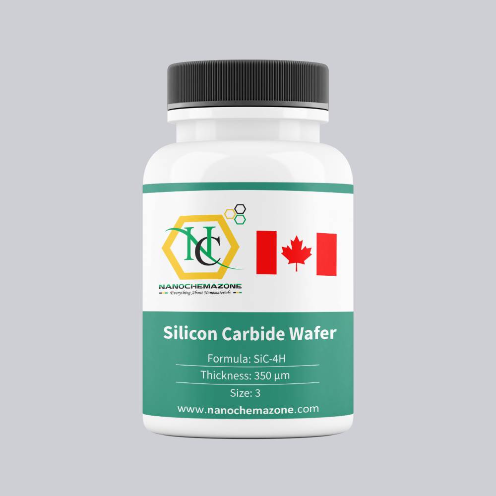
Silicon Carbide Wafer (SiC-4H)- 4H
Size: 4'', Thickness: 350 μm, 4H Area: 95%
Technical Properties:
| Quality |
Testing Grade |
| Size (inch) |
4” |
| Thickness (μm) |
350 |
| Ra |
≤0.3 |
| 4H area |
95% |
| Orientation |
4°±0.5° |
| Resistivity |
0.015-0.03 |
| TTV |
≤25 |
| Bow |
≤30 |
| Warp |
≤35 |
| OF Length |
32.5±2 |
| IF Length |
18±2 |
Fields of Application for Silicon Carbide (SiC-4H) - 4H Wafer
Silicon carbide (SiC) is a rare compound of silicon and carbon which is synthetically produced.
Silicon carbide (SiC) wafer has great electrical properties and excellent thermal properties. Silicon carbide (SiC) wafer has low thermal expansion.
Silicon carbide (SiC) wafer has superior hardness properties. Silicon carbide (SiC) wafer performs well at high temperatures. Also, silicon carbide (SiC)
wafer has high resistance to corrosion, erosion and oxidation. In addition to, silicon carbide (SiC) wafer is also more shiny than either diamonds or
cubic zirconia.
Silicon carbide (SiC) crystals have unique physical and electronic properties. Silicon Carbide based devices have been used for short wavelength opto-electronic, high temperature, radiation resistant applications. The high-power and high-frequency electronic devices made with SiC are superior to Si and GaAs based devices. Below are some popular applications of SiC substrates.
SiC based devices have low lattice mismatch with III-nitride epitaxial layers. They have high thermal conductivity and can be used for the monitoring of combustion processes and for all sorts of UV-detection. SiC-based semiconductor devices can work under very hostile environments, such as high temperature, high power, and high radiation conditions.
SiC is used for the fabrication of very high-voltage and high-power devices such as diodes, power transistors, and high power microwave devices. Compared to conventional Si-devices, SiC-based power devices have faster switching speed higher voltages, lower parasitic resistances, smaller size, less cooling required due to high-temperature capability.
While Silicon carbide (SiC-4H) - 4H wafer has superior electronic properties, silicon carbide (SiC-6H) – 6H wafer is most easily prepared and best studied.
- Silicon carbide (SiC) wafer is used for hybrid and electric vehicles.
- Silicon carbide (SiC) wafer is used for green energy generation.
- Silicon carbide (SiC) wafer is used for LEDs.
- Silicon carbide (SiC) wafer is used for many other emerging markets.