• CONTACT US
  • FAQs
FREE SHIPPING WITHIN CANADA FOR ALL ORDER OF 300$
0 Compare
0 Wishlist
Login / Register
  • Home
  • Products
  • Contact Us
Menu
0 items / $0.00
Browse Categories
  • 3D Printer Materials
  • BATTERY EQUIPMENT
  • CARBON NANOTUBES
  • DISPERSIONS
  • MICROPARTICLES
  • MXene and MAXene
  • NANOPARTICLES & NANOPOWDERS
  • RARE EARTH MATERIALS
  • SILICON WAFERS & SEMICONDUCTOR WAFERS
24/7 SUPPORT

+1-780-612-4177

0 items / $0.00
Click to enlarge
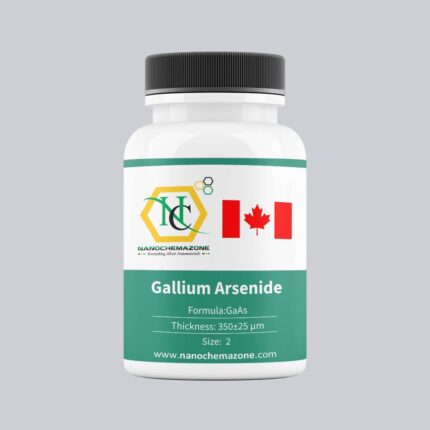
HomeSilicon Wafers & Semiconductor WafersGallium Arsenide (GaAs) Wafers Gallium Arsenide (GaAs) Wafers, Size: 2”, Thickness: 350±25 μm, Single Side Polished, EPI-ready, Mobility: 1000-3000
Previous product
Placeholder
Gallium Arsenide (GaAs) Wafers, Size: 2”, Thickness: 350±25 μm, Double Side Polished, EPI-ready $189.00 – $3,588.00
Back to products
Next product
Silicon on Insulator (SOI) Wafers, Size: 4'', Thickness: 725 μm, P type (Boron doped) $898.00 – $3,936.00

Gallium Arsenide (GaAs) Wafers, Size: 2”, Thickness: 350±25 μm, Single Side Polished, EPI-ready, Mobility: 1000-3000

$189.00 – $3,588.00

Clear
Compare
Add to wishlist
SKU: N/A Category: Gallium Arsenide (GaAs) Wafers
Share
  • Description
  • Additional information
  • Shipping & Delivery
Description

Gallium Arsenide (GaAs) Wafer

Size: 2”, Thickness: 350±25 μm, Mobility: 1000-3000

Technical Properties:

Quality  GaAs
Materials  GaAs
Size (inch)  2”
Thickness (μm)  350± 25
Polished  Single Side
Dopant  Silicon (N type)
Orientation  (100)2 deg off toward <111>A±0.5
Resistivity   (1.2—9.9) E-3
Mobility  1000-3000
EPD  ≤3000
Growth method  VGF
OF Length  17±1
IF Length   7±1

Fields of Application for Gallium Arsenide (GaAs)

Gallium arsenide (GaAs) is a compound of the elements gallium and arsenic.

Gallium arsenide (GaAs) is a semiconductor compound. Gallium arsenide (GaAs)  has a high electron velocity and high saturated electron mobility.
This makes gallium arsenide (GaAs) components are useful in fast electronic switching applications and at ultra-high radio frequencies.

In 1907, the British discovered infrared emmission from gallium arsenide. This was called electroluminescence. Also, gallium arsenide (GaAs) was
used as a solar cells in space for the Venera 3 mission in 1965, which is the first known operational use of gallium arsenide (GaAs).

Vertical gradient freeze is the most common method to produce GaAs wafers.

Mainly used for circuits, electronics and solar cell applications.

Carbon, silicon, tellurium and zinc are some of the dopants that are used to modify the characteristics and electrical properties of gallium arsenide wafers.

Wafer flatness and surface purity are ensured by highest quality standards.

Boron concentration of gallium arsenide wafers highly depend on the production method.

Gallium arsenide wafers with adequate electrical resistancy prevent high current induction in the circuit.

Mobility of GaAs wafers can be tailored with different doping levels.

  • Gallium arsenide (GaAs) is used in laser diodes.
  • Gallium arsenide (GaAs) is used in solar cells.
  • Gallium arsenide (GaAs) is used in optical windows.
  • Gallium arsenide (GaAs) is used in monolithic microwave integrated circuits.
  • Gallium arsenide (GaAs) is used in microwave frequency integrated circuits.
  • Gallium arsenide (GaAs) is used in infrared light-emitting diodes.
  • Gallium arsenide (GaAs) is useful in barometers.
  • Gallium arsenide (GaAs) is useful in pharmaceuticals and nuclear medicine tests.
  • Gallium arsenide (GaAs) is useful in high temperature thermometers.
Additional information
pcs

1 Piece, 25 Piece, 5 Piece

Shipping & Delivery

Related products

Gallium Arsenide (GaAs) Wafers, Size: 4”, Thickness: 350±25 μm, Single Side Polished, EPI-ready

Gallium Arsenide (GaAs) Wafers
$189.00 – $3,588.00
Select options
Compare
Quick view
Add to wishlist
Close

Gallium Arsenide (GaAs) Wafers, Size: 2”, Thickness: 350± 25 μm, Orientation: 100, Single Side Polished, EPI-ready

Gallium Arsenide (GaAs) Wafers
$189.00 – $3,588.00
Select options
Compare
Quick view
Add to wishlist
Close

Gallium Arsenide (GaAs) Wafers, Size: 2”, Thickness: 350±25 μm, Single Side Polished, EPI-ready

Gallium Arsenide (GaAs) Wafers
$162.00 – $3,108.00
Select options
Compare
Quick view
Add to wishlist
Close

Gallium Arsenide (GaAs) Wafer, Size: 4”, Thickness: 300± 25 μm, Double Side Polished, EPI-ready

Gallium Arsenide (GaAs) Wafers
$237.00 – $4,776.00
Select options
Compare
Quick view
Add to wishlist
Close
Placeholder

Gallium Arsenide (GaAs) Wafers, Size: 2”, Thickness: 350±25 μm, Double Side Polished, EPI-ready

Gallium Arsenide (GaAs) Wafers
$189.00 – $3,588.00
Select options
Compare
Quick view
Add to wishlist
Close

FREE SHIPPING

Carrier information.

ONLINE PAYMENT

Payment methods.

24/7 SUPPORT

Unlimited help desk.

100% SAFE

View our benefits.

FREE RETURNS

Track or cancel orders.

  • QUICK LINKS
    • About Us
    • Catalogue
    • Quotation
    • FAQ's
    • Products

  • CATEGORIES
    • MXene and MAXene
    • Wafers
    • Nanoparticles
    • Advanced Nanomaterials
    • Artificial Biological Solutions

  • POLICIES
    • Privacy Policy
    • Returns
    • Terms & Conditions
    • Contact Us
    • Our Sitemap

AVAILABLE ON:

Payment System:
payment
Shipping System:
shipping

©NANOCHEMAZONE @ 2015-24 | All Rights Reserved
  • Menu
  • Categories
  • 3D Printer Materials
  • BATTERY EQUIPMENT
  • CARBON NANOTUBES
  • DISPERSIONS
  • MICROPARTICLES
  • MXene and MAXene
  • NANOPARTICLES & NANOPOWDERS
  • RARE EARTH MATERIALS
  • SILICON WAFERS & SEMICONDUCTOR WAFERS
  • Home
  • Shop
  • Blog
  • About us
  • Wishlist
  • Compare
  • Login / Register
Shopping cart
close

Sign in

close

Lost your password?

No account yet?

Create an Account
Shop
0 Wishlist
0 items Cart
My account