1 piece: 8.4 €
5 pieces: 34 €
10 pieces: 52 €
Coin Style Single Wafer Shipper, 4’’ / 100 mm , Natural PP
 Introduction
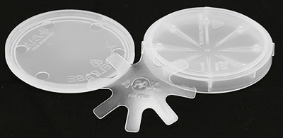
- The wafer shippers are specifically designed to ship, transport or store semiconductor wafers. Primarily designed to hold thin silicon wafers, but are equally suitable for glass, quartz, sapphire, GaAs and other thin round wafers in sizes from Ø2” to 6” or Ø51 to 150mm.
- These wafer shippers/carriers are also known as coin shippers
- They comprise of three parts: base, spider spring and locking cap.
- The inside of the base is concave to ensure that the wafers are held at the edges only.
- The spider spring holds the wafer in place once the cap is locked to the base.
- Available in sizes of 2” to 6” or equivalent 51 to 150mm diameter which a translucent, natural polypropylene
|
Product #
|
Wafer Size
|
Dimensions
|
Material
|
| NG01WS0103 |
4” / 100 mm |
Ø130 x 15 mm |
Natural translucent PP |
WAFER SHIPPER FEATURES
• For shipping and storage of 4'' wafers
• Positive closure
• Holds one wafer facedown
• Wafer face contact is on the edge only
• Eight spring cushion holds the wafer
• Stackable
WAFER SHIPPER SPECIFICATIONS
Polypropylene (PP) Properties:
• Translucent/milky white
• Low dielectric constant (insulating)
• Not hygroscopic (water absorption <0.01%)
• Continuous use temperature limit: 55 C
• Melting temperature: 164 C
• Specific gravity: 0.9g/cm^3
• Chemical resistance: IPA OK, Acetone OK
The “Coin Style” single wafer shippers or wafer holders are available in different sizes and materials (Natural PP). For easy loading/unloading in automated or manual applications. They are impact resistant with a screw-on lid for secure packing.
Single wafer shipping container for safe transporting of your 4" (100 mm) wafers. The coinstyle shippers are cylindrical shaped and usually include a sping (they can also be ordered without a spring). The coin style shippers are designed to absorb impact and have a screw-on lid for secure packing of your wafers.