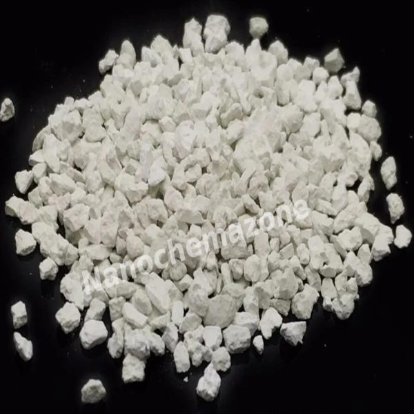
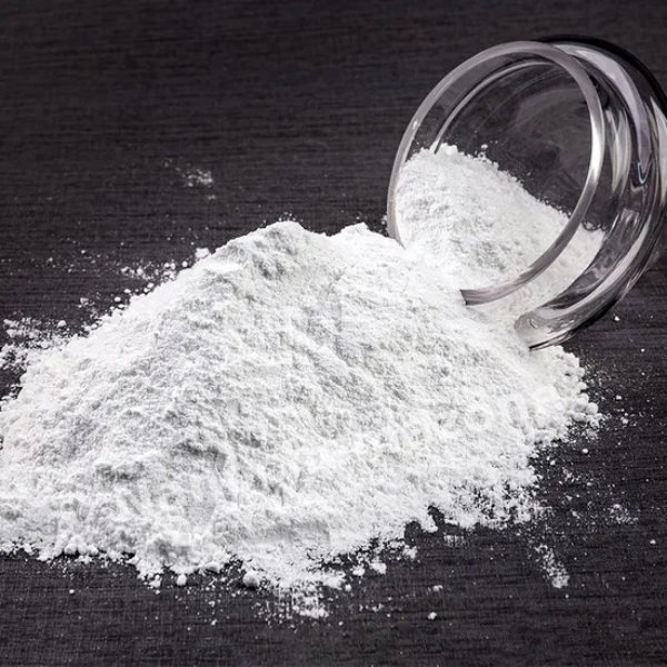
Hexagonal Boron Nitride Nanotube Dia:<50nm, Length:5-20um, 99%
Product description
Boron nitride nanotubes are formed by replacing the C atoms in CNTs with alternating B and N atoms, and do not change the spatial structure of CNTs. Compared with CNT, hexagonal BNNT with graphite-like structure has chemical stability and unique thermal, electrical and optical properties. BN has both high thermal conductivity and low electrical conductivity; it has good thermal shock resistance; even at a high temperature of 1000 °C or in harsh environments, BN is still quite stable and has excellent corrosion resistance; BN's The coefficient of friction is about twice that of graphite and does not change substantially with temperature. Although BNNT cannot be prepared in large quantities at present, due to its good strength, thermal stability and electrical properties, people have made some explorations on the application of BNNT and made certain progress. Compared with CNT, BNNT has better thermal stability, and theoretical calculations show that BNNT has higher defect generation energy, which is still positive under high stress, so it has higher yield resistance; in addition, it also It has higher thermal conductivity and the strength is also the highest among known insulating fibers. Therefore, BNNT as a mechanical reinforcement material will have more advantages than traditional fibers and CNT in terms of strength and oxidation resistance, and BNNT can also be combined with nano-ceramic fibers to form new fiber composite materials. These properties determine the broad application prospects of BN nanomaterials in the fields of nanoelectronics, electronic heat dissipation components, solid/liquid lubricants, nanocomposites and high-temperature structural components.
Performance characteristics
Hexagonal boron nitride nanotubes are prepared by high-frequency plasma gas phase synthesis, and have excellent physical and chemical properties: high temperature resistance, oxidation resistance, chemical corrosion resistance, self-lubricating, good processability, high thermal conductivity, and good medium It is widely used in high-tech fields such as machinery, metallurgy, electronics, aerospace and so on.
Applications
Filling the high thermal conductivity and high stability boron nitride fiber filler into the polymer plastic system can effectively improve the low thermal conductivity and poor thermal stability of the composite material system. Thereby, the high temperature stability and oxidation resistance of the inorganic-organic polymer materials are effectively improved, and the working temperature of the packaged materials, such as LEDs, is effectively reduced, and the working time thereof is prolonged. CB-BNNT as a mechanical reinforcement material will have more advantages than traditional fibers and CNT in terms of strength and oxidation resistance, and CB-BNNT can also be combined with nano-ceramic fibers to form a new fiber composite material. These properties determine the broad application prospects of BN nanomaterials in the fields of nanoelectronics, electronic heat dissipation components, solid/liquid lubricants, nanocomposites and high-temperature structural components.
Packaging and storage
This product is packaged in an inert gas plastic bag, sealed and stored in a dry, cool environment. It should not be exposed to the air to prevent oxidation and agglomeration due to moisture, which will affect the dispersion performance and use effect.