Carbon Nanotubes Doped with 52 wt% Iron Oxide (Fe3O4) Nanopowder/Nanoparticles

Price range: $98.00 through $544.00
Select options This product has multiple variants. The options may be chosen on the product page

Carbon nanotubes doped with metal oxide nanopowders improve electrical and mechanical properties significantly. Hardness, tensile strength, specific strength, and elastic modulus are examples of such enhancements. As a result of these advancements, these materials are now widely used for a variety of purposes.

applications. Among these applications are drug delivery, biosensors, 3-CNT composites, 4-catalysis, 5-nanoprobes, and 6-hydrogen storage. 8 gas-discharge tubes, 7 lithium batteries nine flat panel displays 10-supercapacitors, 11-transistors, twelve solar cells, 13-photoluminescence, 14-templates  

Silicon Carbide (SiC) Nanopowder/Nanoparticles, Beta, Purity: 99.5+%, Size: 50-70 nm

Price range: $44.00 through $544.00
Select options This product has multiple variants. The options may be chosen on the product page
5 grams/39 € 25 grams/56 € 100 grams/97 € 500 grams/295 € 1000 grams/480 €
Please contact us for quotes on larger quantities !!!

Silicon Carbide (SiC) Nanopowder/Nanoparticles

Beta, Purity: 99.5+%, Size: 50-70 nm

Storage Condition:

Silicon Carbide nanoparticles should be sealed in vacuum and stored in cool and dry room. It should not be exposure to air and avoid stress.

Applications:

Silicon carbide nanopowder can be used as a hard and high grade refractory material. It can be used in ceramics such as ceramic besrings, textile ceramics, high frequency ceramics, and ceramic engine parts. It also can be used in hard discs, polishing abrasives, grinding wheels, and as a support for multichip modules. Silicon carbide nanopowder has also high thermal conductivity. It can be used in high temperature sealing valves, high temperature spray nozzles, and high temperature fluid transport parts. It aslo can be used in composites to increase strength and heat resistance.

Copper (Cu) Nanowire, Purity: 99.55%, in Ethanol

Price range: $51.00 through $544.00
Select options This product has multiple variants. The options may be chosen on the product page

Copper (Cu) Nanowire

Purity: 99.55%, in Ethanol

Technical Properties:

Purity (%) 99,55
Color reddish-brown
Average Diameter (nm) 150-200
Length (µm) 4,0-8,0
 

Indium Oxide (In2O3) Sputtering Targets, Purity: 99.99%, Size: 2”, Thickness: 0.125”

$543.00

Product 

Indium Oxide (In2O3) Sputtering Targets, Purity: 99.99%, Size: 2'', Thickness: 0.125''

CAS No.

 1312-43-2

Appearance

Powder

Purity

≥99%,  ≥99.9%,  ≥95%

(Other purities are also available)

APS

< 5 µm (Size Can be customized), Ask for other available size ranges.

Ingredient

N/A

Molecular Weight

 277.64 g/mol

Melting Point

 ~1,910 °C

Boiling Point

 3,000 °C(approx., decomposes)

Density

~7.18 g/cm³ (sintered form)

Product Codes

NCZ-2218K

Tetracalcium phosphate(Ca4(PO4)2O, Biomedicine grade, >98%) (204982)

$542.00
Select options This product has multiple variants. The options may be chosen on the product page

Product 

Tetracalcium phosphate(Ca4(PO4)2O, Biomedicine grade, >98%) (204982)

CAS No.

1306‑01‑0

Appearance

Powder

Purity

≥99%,  ≥99.9%,  ≥95%

(Other purities are also available)

APS

  <80um (Size Can be customized), Ask for other available size ranges.

Ingredient

N/A

Molecular Weight

~366.25 g/mol

Melting Point

Decomposes at ~1450 °C

Boiling Point

N/A

Density

 Not widely documented (but typical calcium phosphates range ~2.9–3.2 g/cm³)

Product Codes

NCZ-2612K

Titanium Dioxide (TiO2) Sputtering Targets, Purity: 99.9%, Size: 4”, Thickness: 0.250”, Grey to Black

$542.00

Applications of Sputtering Targets;

Film deposition is accomplished using sputtering targets. A technique for sputtering thin films is called "deposition made by sputter targets," which entails eroding material from a "target" source onto a "substrate" like a silicon wafer. Etching of the target is done using semiconductor sputtering targets. When selectivity is not an issue and a high degree of etching anisotropy is required, sputter etching is the method of choice. By removing the target material through etching, sputter targets are also utilized for investigation. In secondary ion spectroscopy (SIMS), one example is when the target material is sputtered at a steady pace. Mass spectrometry is used to quantify the concentration and identity of spewed atoms as the target is sputtered.

The target material's composition may be ascertained and even very low concentrations of contaminants can be found with the aid of the sputtering target.

There is also an application area for sputtering targets in space. One type of space weathering that alters the chemical and physical characteristics of airless worlds like the Moon and asteroids is sputtering.

Tin Oxide (SnO2) Sputtering Targets, Purity: 99.99%, Size: 1”, Thickness: 0.125”

$542.00

Applications of Sputtering Targets;

Film deposition is accomplished using sputtering targets. A technique for sputtering thin films is called "deposition made by sputter targets," which entails eroding material from a "target" source onto a "substrate" like a silicon wafer. Etching of the target is done using semiconductor sputtering targets. When selectivity is not an issue and a high degree of etching anisotropy is required, sputter etching is the method of choice. By removing the target material through etching, sputter targets are also utilized for investigation. In secondary ion spectroscopy (SIMS), one example is when the target material is sputtered at a steady pace. Mass spectrometry is used to quantify the concentration and identity of spewed atoms as the target is sputtered.

Even very low quantities of contaminants can be detected with the aid of the sputtering target, allowing for the determination of the target material's composition.

Applications for sputtering targets are also found in space. One type of space weathering is sputtering, which modifies the chemical and physical characteristics of airless worlds like the Moon and asteroids.

Tin (Sn) Sputtering Targets, Purity: 99.99%, Size: 6”, Thickness: 0.250”

$542.00

Applications of Sputtering Targets;

Film deposition is accomplished using sputtering targets. A technique for sputtering thin films is called "deposition made by sputter targets," which entails eroding material from a "target" source onto a "substrate" like a silicon wafer. Etching of the target is done using semiconductor sputtering targets. When selectivity is not an issue and a high degree of etching anisotropy is required, sputter etching is the method of choice. By removing the target material through etching, sputter targets are also utilized for investigation. In secondary ion spectroscopy (SIMS), one example is when the target material is sputtered at a steady pace. Mass spectrometry is used to quantify the concentration and identity of spewed atoms as the target is sputtered.

The target material's composition may be ascertained and even very low concentrations of contaminants can be found with the aid of the sputtering target.

There is also an application area for sputtering targets in space. One type of space weathering that alters the chemical and physical characteristics of airless worlds like the Moon and asteroids is sputtering.

Lithium Niobate (LiNbO3) Sputtering Targets, Purity: 99.9%, Size: 2”, Thickness: 0.250”

$542.00

Applications of Sputtering Targets;

Film deposition is accomplished using sputtering targets. A technique for sputtering thin films is called "deposition made by sputter targets," which entails eroding material from a "target" source onto a "substrate" like a silicon wafer. Etching of the target is done using semiconductor sputtering targets. When selectivity is not an issue and a high degree of etching anisotropy is required, sputter etching is the method of choice. By removing the target material through etching, sputter targets are also utilized for investigation. In secondary ion spectroscopy (SIMS), one example is when the target material is sputtered at a steady pace. Mass spectrometry is used to quantify the concentration and identity of spewed atoms as the target is sputtered.

By helping of the sputtering target, the composition of the target material may be evaluated and even extremely tiny amounts of contaminants are recognized.

There is also an application area for sputtering targets in space. One type of space weathering that alters the chemical and physical characteristics of airless worlds like the Moon and asteroids is sputtering.

Lithium Nickel Cobalt Oxide (LiNi(1-x)CoxO2) Sputtering Targets, Purity: 99.9%, Size: 2”, Thickness: 0.125”

$542.00

Applications of Sputtering Targets;

Film deposition is accomplished using sputtering targets. A technique for sputtering thin films is called "deposition made by sputter targets," which entails eroding material from a "target" source onto a "substrate" like a silicon wafer. Etching of the target is done using semiconductor sputtering targets. When selectivity is not an issue and a high degree of etching anisotropy is required, sputter etching is the method of choice. By removing the target material through etching, sputter targets are also utilized for investigation. In secondary ion spectroscopy (SIMS), one example is when the target material is sputtered at a steady pace. Mass spectrometry is used to quantify the concentration and identity of spewed atoms as the target is sputtered.

By helping of the sputtering target, the composition of the target material may be evaluated and even extremely tiny amounts of contaminants are recognized.

There is also an application area for sputtering targets in space. One type of space weathering that alters the chemical and physical characteristics of airless worlds like the Moon and asteroids is sputtering.

Formula LiCoO2 represents the chemical compound lithium cobalt oxide. A crystalline solid that is dark blue or bluish-gray in color, lithium cobalt oxide is frequently utilized in the positive electrodes of lithium-ion batteries.

Vanadium Oxide (V2O5) Sputtering Targets, Purity: 99.9%, Size: 4”, Thickness: 0.250”

$541.00

Applications of Sputtering Targets;

Film deposition is accomplished using sputtering targets. A technique for sputtering thin films is called "deposition made by sputter targets," which entails eroding material from a "target" source onto a "substrate" like a silicon wafer. Etching of the target is done using semiconductor sputtering targets. When selectivity is not an issue and a high degree of etching anisotropy is required, sputter etching is the method of choice. By removing the target material through etching, sputter targets are also utilized for investigation. In secondary ion spectroscopy (SIMS), one example is when the target material is sputtered at a steady pace. Mass spectrometry is used to quantify the concentration and identity of spewed atoms as the target is sputtered.

The target material's composition may be ascertained and even very low concentrations of contaminants can be found with the aid of the sputtering target.

There is also an application area for sputtering targets in space. One type of space weathering that alters the chemical and physical characteristics of airless worlds like the Moon and asteroids is sputtering.

Selenium (Se) Micron Powder Purity: 99.9%, Size: 325 mesh

Price range: $27.00 through $541.00
Select options This product has multiple variants. The options may be chosen on the product page
5 grams/24 € 25 grams/56 €                        
100 grams/122 €                     
500 grams/295 €                     
1000 grams/490 €

Purity: 99.9%, Size: 325 mesh

Magnesium carbonate whisker(MgCO3, ≥98%, D=1-2um, L=20-60um) (125665)

$540.00
Select options This product has multiple variants. The options may be chosen on the product page
Magnesium carbonate whisker(MgCO3, ≥98%, D=1-2um, L=20-60um) (125665)


MgO

≥47.3%

Length-Diameter ratio

20-50

Length/um

20-60

Diameter/um

1-2

 
Product Codes- NCZ-2752K

Niobium Oxide (Nb2O5) Sputtering Targets, indium, Purity: 99.5%, Size: 4”, Thickness: 0.125”

$540.00

Product 

Niobium Oxide (Nb2O5) Sputtering Targets, indium, Purity: 99.5%, Size: 4'', Thickness: 0.125''

CAS No.

1313-96-8

Appearance

Powder

Purity

≥99%,  ≥99.9%,  ≥95%

(Other purities are also available)

APS

N/A (Size Can be customized), Ask for other available size ranges.

Ingredient

N/A

Molecular Weight

 265.81 g/mol

Melting Point

~1512 °C

Boiling Point

N/A

Density

 4.6 – 4.9 g/cm³

Product Codes

NCZ-1802K

Tungsten (W) Sputtering Targets, elastomer, Purity: 99.95%, Size: 2”, Thickness: 0.125”

$540.00

Product 

Tungsten (W) Sputtering Targets, elastomer, Purity: 99.95%, Size: 2'', Thickness: 0.125''

CAS No.

7440-33-7

Appearance

Powder

Purity

≥99%,  ≥99.9%,  ≥95%

(Other purities are also available)

APS

N/A  (Size Can be customized), Ask for other available size ranges.

Ingredient

N/A

Molecular Weight

 183.84 g/mol

Melting Point

3422 °C

Boiling Point

 5555 °C

Density

19.25 g/cm³

Product Codes

NCZ-1584K

Vanadium Oxide (V2O5) Sputtering Targets, Purity: 99.9%, Size: 3”, Thickness: 0.125”

$540.00

Product 

Vanadium Oxide (V2O5) Sputtering Targets, Purity: 99.9%, Size: 3'', Thickness: 0.125''

CAS No.

1314‑62‑1

Appearance

Powder

Purity

≥99%,  ≥99.9%,  ≥95%

(Other purities are also available)

APS

N/A  (Size Can be customized), Ask for other available size ranges.

Ingredient

N/A

Molecular Weight

181.88 g/mol

Melting Point

690 °C

Boiling Point

~1750 °C

Density

~3.35 g/cm³

Product Codes

NCZ-1539K

Vanadium (V) Sputtering Targets, Purity: 99.5%, Size: 8”, Thickness: 0.250”

$540.00

Applications of Sputtering Targets;

Film deposition is accomplished using sputtering targets. A technique for sputtering thin films is called "deposition made by sputter targets," which entails eroding material from a "target" source onto a "substrate" like a silicon wafer. Etching of the target is done using semiconductor sputtering targets. When selectivity is not an issue and a high degree of etching anisotropy is required, sputter etching is the method of choice. By removing the target material through etching, sputter targets are also utilized for investigation. In secondary ion spectroscopy (SIMS), one example is when the target material is sputtered at a steady pace. Mass spectrometry is used to quantify the concentration and identity of spewed atoms as the target is sputtered.

The target material's composition may be ascertained and even very low concentrations of contaminants can be found with the aid of the sputtering target.

There is also an application area for sputtering targets in space. One type of space weathering that alters the chemical and physical characteristics of airless worlds like the Moon and asteroids is sputtering.

Tungsten (W) Sputtering Targets, Purity: 99.95%, Size: 6”, Thickness: 0.250”

$540.00

Applications of Sputtering Targets;

Film deposition is accomplished using sputtering targets. A technique for sputtering thin films is called "deposition made by sputter targets," which entails eroding material from a "target" source onto a "substrate" like a silicon wafer. Etching of the target is done using semiconductor sputtering targets. When selectivity is not an issue and a high degree of etching anisotropy is required, sputter etching is the method of choice. By removing the target material through etching, sputter targets are also utilized for investigation. In secondary ion spectroscopy (SIMS), one example is when the target material is sputtered at a steady pace. Mass spectrometry is used to quantify the concentration and identity of spewed atoms as the target is sputtered.

The target material's composition may be ascertained and even very low concentrations of contaminants can be found with the aid of the sputtering target.

There is also an application area for sputtering targets in space. One type of space weathering that alters the chemical and physical characteristics of airless worlds like the Moon and asteroids is sputtering.

Magnesium Fluoride (MgF2) Sputtering Targets, Purity: 99.9%, Size: 2”, Thickness: 0.250′

$540.00

Applications of Sputtering Targets;

Film deposition is accomplished using sputtering targets. A technique for sputtering thin films is called "deposition made by sputter targets," which entails eroding material from a "target" source onto a "substrate" like a silicon wafer. Etching of the target is done using semiconductor sputtering targets. When selectivity is not an issue and a high degree of etching anisotropy is required, sputter etching is the method of choice. By removing the target material through etching, sputter targets are also utilized for investigation. In secondary ion spectroscopy (SIMS), one example is when the target material is sputtered at a steady pace. Mass spectrometry is used to quantify the concentration and identity of spewed atoms as the target is sputtered.

By helping of the sputtering target, the composition of the target material may be evaluated and even extremely tiny amounts of contaminants are recognized.

There is also an application area for sputtering targets in space. One type of space weathering that alters the chemical and physical characteristics of airless worlds like the Moon and asteroids is sputtering.

Zinc (Zn) Nanopowder/Nanoparticles, Purity: 99.95%,Size: 790 nm

Price range: $21.57 through $539.14
Select options This product has multiple variants. The options may be chosen on the product page
Zinc (Zn) Nanopowder/Nanoparticles Purity: 99.95%, Size: 790 nm Technical Properties: True Density (g/cm3) 7,1 Color dark gray Tmelting (oC) 420 Tboiling (oC)

Ultra Fine Magnetic Fe3O4 Nanoparticle for Biomolecular Coupling, 2-5nm

Price range: $286.00 through $539.00
Select options This product has multiple variants. The options may be chosen on the product page
Product Ultra Fine Magnetic Fe3O4 Nanoparticle for Biomolecular Coupling, 2-5nm
CAS No. 1317-61-9
Appearance Brown
Purity ≥99%,  ≥99.9%,  ≥95%(Other purities are also available)
APS 2-5nm (Size Can be customized),  Ask for other available size range.
Ingredient Fe3O4
Molecular Weight 231.53 g/mol
Melting Point N/A
Boiling Point N/A
Density 5.0–5.17 g/cm³
Product Codes NCZ-590I
 

Titanium Aluminum Carbonitride (Ti3AlCN) MAX Phase Micron-Powder, 1-40um, 10g

$539.00
Product Titanium Aluminum Carbonitride (Ti3AlCN) MAX Phase Micron-Powder, 1-40um, 10g
CAS No. N/A
Appearance Dark grey to black
Purity ≥99%,  ≥99.9%,  ≥95%(Other purities are also available)
APS 1-40um (Size Can be customized),  Ask for other available size range.
Ingredient Ti3AlCN
Molecular Weight 196.60 g/mol
Melting Point N/A
Boiling Point N/A
Density N/A
Product Codes NCZ-572I
 

High Purity Titanium Aluminum Carbide (Ti2AlC) MAX Phase Micron-Powder, 10g

Price range: $506.00 through $539.00
Select options This product has multiple variants. The options may be chosen on the product page
Product High Purity Titanium Aluminum Carbide (Ti2AlC) MAX Phase Micron-Powder, 10g
CAS No. 1446365-12-5
Appearance Gray to black fine
Purity ≥99%,  ≥99.9%,  ≥95%(Other purities are also available)
APS N/A
Ingredient Ti2AlC
Molecular Weight 171.78 g/mol
Melting Point N/A
Boiling Point N/A
Density 4.1 g/cm³
Product Codes NCZ-414I

99.95% Manganese (Mn) Micron Powder (-320 Mesh), 1kg

$539.00
Product 99.95% Manganese (Mn) Micron Powder (-320 Mesh), 1kg
CAS No. 7439-96-5
Appearance Gray to silvery metallic
Purity ≥99%,  ≥99.9%,  ≥95%(Other purities are also available)
APS 44µm  (Size Can be customized),  Ask for other available size range.
Ingredient Mn
Molecular Weight 54.94 g/mol
Melting Point 1246 °C
Boiling Point 2061 °C
Density 2.1–3.5 g/cm³
Product Codes NCZ-233I

99.9% Monoclinic Zirconia Polishing Powder Nanoparticles, 1kg

Price range: $143.00 through $539.00
Select options This product has multiple variants. The options may be chosen on the product page
Product 99.9% Monoclinic Zirconia Polishing Powder Nanoparticles, 1kg
CAS No. 1314-23-4
Appearance White
Purity ≥99%,  ≥99.9%,  ≥95%(Other purities are also available)
APS 20–100nm (Size Can be customized),  Ask for other available size range.
Ingredient ZrO₂
Molecular Weight 123.22 g/mol
Melting Point 2715 °C
Boiling Point N/A
Density 5.68 g/cm³
Product Codes NCZ-230I

Magnesium Sputtering Target Mg

Price range: $94.00 through $539.00
Select options This product has multiple variants. The options may be chosen on the product page
Product Magnesium Sputtering Target Mg
CAS No. 7439-95-4
Appearance Shiny grey-white metallic
Purity ≥99%,  ≥99.9%,  ≥95%(Other purities are also available)
APS N/A
Ingredient Mg
Molecular Weight 40.30 g/mol
Melting Point 650.0 °C
Boiling Point 1107.0 °C
Density 3.58 g/cm³
Product Codes NCZ-127H
 

Molybdenum Oxide (MoO3) Nanopowder/Nanoparticles, High Purity: 99.96+%, Size: 8-75 nm

Price range: $35.00 through $539.00
Select options This product has multiple variants. The options may be chosen on the product page
1 gram/31 € 5 grams/60 €    
25 grams/175 € 100 grams/475 €
 
Please contact us for quotes on larger quantities !!! 

Molybdenum Oxide (MoO3) Nanopowder/Nanoparticles

High Purity: 99.96+%, Size: 8-75 nm

Technical Properties:

Purity (%) 99.96
Color white-light gray
Average Particle Size (nm) 8.0-75.0
Specific Surface Area (m2/g)    >40
Molecular Weight (g/mol) 143.9
Elemental Analysis (%) Fe Ni Cu Cr Co
0.0012 0.0002 0.023 0.0012 0.00006

Applications:

Molybdenum oxide nanoparticles are widely used in catalysis. It is used as catalysts, cracking catalysts, and hydrogenation catalysts. It is a component of the co-catalyst used in the industrial production of acrylonitrile by the oxidation of propane and ammonia. It is also used in glass and ceramics production.  

Copper Indium (Cu-In) Alloy Nanopowder/Nanoparticles, Purity: 99.9% , Size: < 500 nm

Price range: $121.00 through $539.00
Select options This product has multiple variants. The options may be chosen on the product page
1 gram/107 € 
5 grams/475 €                       
Please contact us for quotes on larger quantities !!! 

Copper Indium (Cu-In) Alloy Nanopowder/Nanoparticles

Purity: 99.9% , Size: < 500 nm

Technical Properties:

Alloy Ratio (Cu-In) depends on customer needs
Average Particle Size (nm) <500

Properties, Storage and Cautions:

Cu-In alloy nanoparticles are highly reactive, therefore it should be handled with care and rapid moves, vibrations should be avoided. The powder should be kept away from sunlight, any kind of heating, moisture and impacts. Coagulation of the particles is a serious problem, so, the powder should be sealed under vacuum and should be kept in cool and dry conditions. Air contact should be avoided.

Copper Indium (Cu-In) Alloy Nanopowder/Nanoparticles, Purity: 99.9% , Size: < 500 nm

Price range: $121.00 through $539.00
Select options This product has multiple variants. The options may be chosen on the product page

Copper Indium (Cu-In) Alloy Nanopowder/Nanoparticles

Purity: 99.9% , Size: < 500 nm

Technical Properties:

Alloy Ratio (Cu-In) depends on customer needs
Average Particle Size (nm) <500

Properties, Storage and Cautions:

Cu-In alloy nanoparticles are highly reactive, therefore it should be handled with care and rapid moves, vibrations should be avoided. The powder should be kept away from sunlight, any kind of heating, moisture and impacts. Coagulation of the particles is a serious problem, so, the powder should be sealed under vacuum and should be kept in cool and dry conditions. Air contact should be avoided.

Chromium (Cr) Nanopowder/Nanoparticles, Purity: 99.95%, Size: 30-40 nm, Metal Basis

Price range: $208.00 through $539.00
Select options This product has multiple variants. The options may be chosen on the product page

Chromium (Cr) Nanopowder/Nanoparticles

Purity: 99.95%, Size: 30-40 nm, Metal Basis

Technical Properties:

Bulk Density (g/cm3) 0,15
True Density (g/cm3) 8,9
Color black
Average Particle Size (nm) 30-40
Specific Surface Area (m2/g) 10,0-40,0
Elemental Analysis Cr Fe Al Si Others
99.9 0.05 0.02 0.01 ≤0.01

Properties, Storage and Cautions:

Chromium nanopowder is highly reactive and flammable, therefore it should be handled with care and rapid moves, vibrations should be avoided. Powder should be kept away from sunlight, any kind of heating, moisture and impacts. Coagulation of the particles is a serious problem, so, Cr powder should be sealed under vacuum and should be kept in cool and dry conditions. Air contact should be avoided.

Applications:

Chromium is a very hard metal. Therefore, in nanopowder form,  it can be widely used in applications where mechanical strength is required. It can be used in ceramics, cutting and shaping tools and steel industry

Copper Indium (Cu-In) Alloy Nanopowder/Nanoparticles, Purity: 99.9% , Size: < 500 nm

Price range: $121.00 through $539.00
Select options This product has multiple variants. The options may be chosen on the product page

Copper Indium (Cu-In) Alloy Nanopowder/Nanoparticles

Purity: 99.9% , Size: < 500 nm

Technical Properties:

Alloy Ratio (Cu-In) depends on customer needs
Average Particle Size (nm) <500

Properties, Storage and Cautions:

Cu-In alloy nanoparticles are highly reactive, therefore it should be handled with care and rapid moves, vibrations should be avoided. The powder should be kept away from sunlight, any kind of heating, moisture and impacts. Coagulation of the particles is a serious problem, so, the powder should be sealed under vacuum and should be kept in cool and dry conditions. Air contact should be avoided.

Indium (In) Sputtering Targets, Purity: 99.99%, Size: 4”, Thickness: 0.125”

$538.00

Product 

Indium (In) Sputtering Targets, Purity: 99.99%, Size: 4'', Thickness: 0.125''

CAS No.

 7440-74-6

Appearance

Powder

Purity

≥99%,  ≥99.9%,  ≥95%

(Other purities are also available)

APS

 N/A (Size Can be customized), Ask for other available size ranges.

Ingredient

N/A

Molecular Weight

114.82 g/mol

Melting Point

 156.6 °C

Boiling Point

 2,072 °C

Density

 7.31 g/cm³

Product Codes

NCZ-2223K

Lanthanum Titanate (LaTiO3) Sputtering Targets, Purity: 99.9%, Size: 1”, Thickness: 0.125”

$538.00

Product 

Lanthanum Titanate (LaTiO3) Sputtering Targets, Purity: 99.9%, Size: 1'', Thickness: 0.125''

CAS No.

12031‑47‑9 (specific to size) or 12201‑04‑6 (general LaTiO₃)

Appearance

Powder

Purity

≥99%,  ≥99.9%,  ≥95%

(Other purities are also available)

APS

<5 µm (Size Can be customized), Ask for other available size ranges.

Ingredient

N/A

Molecular Weight

 234.77 g/mol (exact ~234.839 g/mol)

Melting Point

 Approx. 2,200 °C

Boiling Point

N/A

Density

N/A

Product Codes

NCZ-2094K

Silicon Nitride (Si3N4) Sputtering Targets, Purity: 99.5%, Size: 2”, Thickness: 0.250”, Dark Gray to Black

$538.00

Product 

Silicon Nitride (Si3N4) Sputtering Targets, Purity: 99.5%, Size: 2'', Thickness: 0.250'', Dark Gray to Black

CAS No.

 12033-89-5

Appearance

Powder

Purity

≥99%,  ≥99.9%,  ≥95%

(Other purities are also available)

APS

N/A  (Size Can be customized), Ask for other available size ranges.

Ingredient

N/A

Molecular Weight

 140.28 g/mol

Melting Point

 ~1900 °C

Boiling Point

N/A

Density

~3.2 g/cm³

Product Codes

NCZ-1699K

Ytterbium Oxide (Yb2O3) Sputtering Targets, Purity: 99.99%, Size: 2”, Thickness: 0.125”

$538.00

Applications of Sputtering Targets;

  • Sputtering targets is used for film deposition. The deposition made by sputter targets is a method of depositing thin films by sputtering that involves eroding material from a "target" source onto a "substrate" such as  a silicon wafer.
  • Semiconductor sputtering targets is used to etch the target. Sputter etching is chosen in cases where a high degree of etching anisotropy is needed and selectivity is not a concern.
  • Sputter targets is also used for analysis by etching away the target material.
One of the example occurs in secondary ion spectroscopy (SIMS), where the target sample is sputtered at a constant rate. As the target is sputtered, the concentration and identity of sputtered atoms are measured using mass spectrometry. By helping of the sputtering target, the composition of the target material can be determined and even extremely low concentrations of impurities are detected. Sputtering target has also application area in space. Sputtering is one of the forms of space weathering, a process that changes the physical and chemical properties of airless bodies, such as asteroids and the Moon.

Boron Carbide (B4C) Nanopowder/Nanoparticles, Purity: 99.5+%, Size: 40-60 nm, Hexagonal

Price range: $37.00 through $538.00
Select options This product has multiple variants. The options may be chosen on the product page
1 gram/33 € 5 grams/101 € 25 grams/180 € 100 grams/475 €      
Please contact us for quotes on larger quantities !!!

Storage Condition:

Boron nitride nanoparticles should be sealed in vacuum and stored in cool and dry room. It should not be exposure to air and avoid stress.

Applications:

Boron carbide nanoparticles is one of the most stable and hard materials. It does not react with acid or alkali solutions. It is used as an abrasive in polishing and lapping applications, and also as a loose abrasive in cutting applications such as water jet cutting. Boron carbide has ability of absorbing neutrons without forming long lives radiations. It is used in nuclear applications for shielding, and in control rod, and shut down pellets.  

Copper Indium (Cu-In) Alloy Nanopowder/Nanoparticles, Purity: 99.9% , Size: < 500 nm

Price range: $121.00 through $538.00
Select options This product has multiple variants. The options may be chosen on the product page

Copper Indium (Cu-In) Alloy Nanopowder/Nanoparticles

Purity: 99.9% , Size: < 500 nm

Technical Properties:

Alloy Ratio (Cu-In) depends on customer needs
Average Particle Size (nm) <500

Properties, Storage and Cautions:

Cu-In alloy nanoparticles are highly reactive, therefore it should be handled with care and rapid moves, vibrations should be avoided. The powder should be kept away from sunlight, any kind of heating, moisture and impacts. Coagulation of the particles is a serious problem, so, the powder should be sealed under vacuum and should be kept in cool and dry conditions. Air contact should be avoided.

Manganese (Mn) Sputtering Targets, Purity: 99.95%, Size: 4”, Thickness: 0.125”

$537.00

Product 

Manganese (Mn) Sputtering Targets, Purity: 99.95%, Size: 4'', Thickness: 0.125''

CAS No.

 7439-96-5

Appearance

Powder

Purity

≥99%,  ≥99.9%,  ≥95%

(Other purities are also available)

APS

 N/A (Size Can be customized), Ask for other available size ranges.

Ingredient

N/A

Molecular Weight

54.93804 g/mol

Melting Point

 1,246 °C

Boiling Point

 2,061 °C

Density

 7.21 g/cm³

Product Codes

NCZ-1948K

Manganese (Mn) Sputtering Targets, Purity: 99.95%, Size: 4”, Thickness: 0.250”

$537.00

Product 

Manganese (Mn) Sputtering Targets, Purity: 99.95%, Size: 4'', Thickness: 0.250''

CAS No.

 7439-96-5

Appearance

Powder

Purity

≥99%,  ≥99.9%,  ≥95%

(Other purities are also available)

APS

 N/A (Size Can be customized), Ask for other available size ranges.

Ingredient

N/A

Molecular Weight

54.93804 g/mol

Melting Point

 1,246 °C

Boiling Point

 2,061 °C

Density

 7.21 g/cm³

Product Codes

NCZ-1947K

Molybdenum Disilicide (MoSi2) Sputtering Targets, Purity: 99.95%, Size: 4”, Thickness: 0.125”

$537.00

Product 

Molybdenum Disilicide (MoSi2) Sputtering Targets, Purity: 99.95%, Size: 4'', Thickness: 0.125''

CAS No.

12136-78-6

Appearance

Powder

Purity

≥99%,  ≥99.9%,  ≥95%

(Other purities are also available)

APS

 N/A (Size Can be customized), Ask for other available size ranges.

Ingredient

N/A

Molecular Weight

152.11 g/mol

Melting Point

 ~2030 °C

Boiling Point

 ~2300 °C to 2500 °C

Density

~6.26 g/cm³

Product Codes

NCZ-1923K

Molybdenum Oxide (MoO3) Sputtering Targets, Purity: 99.9%, Size: 4”, Thickness: 0.125”

$537.00

Product 

Molybdenum Oxide (MoO3) Sputtering Targets, Purity: 99.9%, Size: 4'', Thickness: 0.125''

CAS No.

1313-27-5

Appearance

Powder

Purity

≥99%,  ≥99.9%,  ≥95%

(Other purities are also available)

APS

 N/A (Size Can be customized), Ask for other available size ranges.

Ingredient

N/A

Molecular Weight

 143.94 g/mol

Melting Point

 ~795°C

Boiling Point

 ~1155°C

Density

 ~4.7 g/cm³

Product Codes

NCZ-1899K

Selenium (Se) Sputtering Targets, Purity: 99.999%, Size: 4”, Thickness: 0.250”

$537.00

Applications of Sputtering Targets;

Film deposition is accomplished using sputtering targets. A technique for sputtering thin films is called "deposition made by sputter targets," which entails eroding material from a "target" source onto a "substrate" like a silicon wafer. Etching of the target is done using semiconductor sputtering targets. When selectivity is not an issue and a high degree of etching anisotropy is required, sputter etching is the method of choice. By removing the target material through etching, sputter targets are also utilized for investigation. In secondary ion spectroscopy (SIMS), one example is when the target material is sputtered at a steady pace. Mass spectrometry is used to quantify the concentration and identity of spewed atoms as the target is sputtered.

The target material's composition may be ascertained and even very low concentrations of contaminants can be found with the aid of the sputtering target.

There is also an application area for sputtering targets in space. One type of space weathering that alters the chemical and physical characteristics of airless worlds like the Moon and asteroids is sputtering.

Magnesium Oxide (MgO) Sputtering Targets, Purity: 99.95%, Size: 5”, Thickness: 0.125”

$537.00

Applications of Sputtering Targets;

Film deposition is accomplished using sputtering targets. A technique for sputtering thin films is called "deposition made by sputter targets," which entails eroding material from a "target" source onto a "substrate" like a silicon wafer. Etching of the target is done using semiconductor sputtering targets. When selectivity is not an issue and a high degree of etching anisotropy is required, sputter etching is the method of choice. By removing the target material through etching, sputter targets are also utilized for investigation. In secondary ion spectroscopy (SIMS), one example is when the target material is sputtered at a steady pace. Mass spectrometry is used to quantify the concentration and identity of spewed atoms as the target is sputtered.

By helping of the sputtering target, the composition of the target material may be evaluated and even extremely tiny amounts of contaminants are recognized.

There is also an application area for sputtering targets in space. One type of space weathering that alters the chemical and physical characteristics of airless worlds like the Moon and asteroids is sputtering.

Lanthanum Calcium Manganate (La0.7Ca0.3MnO3) Sputtering Targets, Purity: 99.9%, Size: 4”, Thickness: 0.250”

$536.00

Product 

Lanthanum Calcium Manganate (La0.7Ca0.3MnO3) Sputtering Targets, Purity: 99.9%, Size: 4'', Thickness: 0.250''

CAS No.

123273‑09‑6

Appearance

Powder

Purity

≥99%,  ≥99.9%,  ≥95%

(Other purities are also available)

APS

 N/A (Size Can be customized), Ask for other available size ranges.

Ingredient

N/A

Molecular Weight

 ~313.9 g/mol

Melting Point

 ~1,550 °C (approximate; ceramic decomposition likely above)

Boiling Point

N/A

Density

 ~5.3 g/cm³ @ room temp

Product Codes

NCZ-2151K

Zinc Oxide (ZnO) with Alumina Sputtering Targets, Purity: 99.99%, Size: 4”, Thickness: 0.125”

$536.00

Applications of Sputtering Targets;

Film deposition is accomplished using sputtering targets. A technique for sputtering thin films is called "deposition made by sputter targets," which entails eroding material from a "target" source onto a "substrate" like a silicon wafer. Etching of the target is done using semiconductor sputtering targets. When selectivity is not an issue and a high degree of etching anisotropy is required, sputter etching is the method of choice. By removing the target material through etching, sputter targets are also utilized for investigation. In secondary ion spectroscopy (SIMS), one example is when the target material is sputtered at a steady pace. Mass spectrometry is used to quantify the concentration and identity of spewed atoms as the target is sputtered.

The target material's composition may be ascertained and even very low concentrations of contaminants can be found with the aid of the sputtering target.

There is also an application area for sputtering targets in space. One type of space weathering that alters the chemical and physical characteristics of airless worlds like the Moon and asteroids is sputtering.

Boron Carbide (B4C) Sputtering Targets, Purity: 99.5%, Size: 8”, Thickness: 0.125”

$536.00

Applications of Sputtering Targets;

Film deposition is accomplished using sputtering targets. A technique for sputtering thin films is called "deposition made by sputter targets," which entails eroding material from a "target" source onto a "substrate" like a silicon wafer. Etching of the target is done using semiconductor sputtering targets. When selectivity is not an issue and a high degree of etching anisotropy is required, sputter etching is the method of choice. By removing the target material through etching, sputter targets are also utilized for investigation. In secondary ion spectroscopy (SIMS), one example is when the target material is sputtered at a steady pace. Mass spectrometry is used to quantify the concentration and identity of spewed atoms as the target is sputtered.

The target material's composition may be ascertained and even very low concentrations of contaminants can be found with the aid of the sputtering target.

There is also an application area for sputtering targets in space. One type of space weathering that alters the chemical and physical characteristics of airless worlds like the Moon and asteroids is sputtering.

Aluminum Oxide (Al2O3) Sputtering Targets, Purity: 99.999%, Size: 2”, Thickness: 0.250”

$536.00

Applications of Sputtering Targets;

Film deposition is accomplished using sputtering targets. A technique for sputtering thin films is called "deposition made by sputter targets," which entails eroding material from a "target" source onto a "substrate" like a silicon wafer. Etching of the target is done using semiconductor sputtering targets. When selectivity is not an issue and a high degree of etching anisotropy is required, sputter etching is the method of choice. By removing the target material through etching, sputter targets are also utilized for investigation. In secondary ion spectroscopy (SIMS), one example is when the target material is sputtered at a steady pace. Mass spectrometry is used to quantify the concentration and identity of spewed atoms as the target is sputtered. With the sputtering target's assistance, the

It is possible to identify the target material and even detect incredibly tiny impurity amounts.

There is also an application area for sputtering targets in space. One type of space weathering that alters the chemical and physical characteristics of airless worlds like the Moon and asteroids is sputtering.

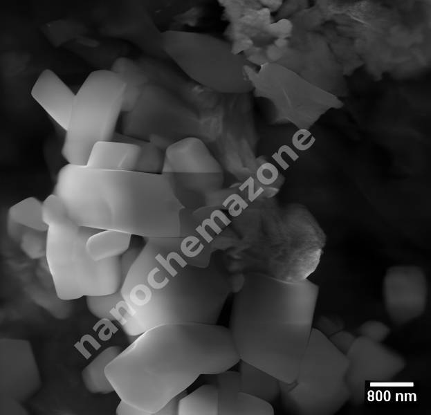
With the chemical formula Al2O3, aluminum oxide is a compound made of aluminum and oxygen. Because of its high melting point, Al2O3 is useful as a refractory material and as an abrasive due to its hardness, as well as for the production of aluminum metal.

Thulium Oxide (Tm2O3) 99.999% 5N High Purity Powder

Price range: $315.00 through $535.00
Select options This product has multiple variants. The options may be chosen on the product page
Product Thulium Oxide (Tm2O3) 99.999% 5N High Purity Powder
CAS No. 12036-44-1
Appearance White to pale green
Purity ≥99%,  ≥99.9%,  ≥95%(Other purities are also available)
APS 5µm (Size Can be customized),  Ask for other available size range.
Ingredient Tm2O3
Molecular Weight 385.87 g/mol
Melting Point 2341 °C
Boiling Point 3945 °C
Density 8.6 g/cm³
Product Codes NCZ-559I

Erbium (III) Oxide (Er2O3) 99.995% 4N5 High Purity Powder, 100g

$535.00
Product Erbium (III) Oxide (Er2O3) 99.995% 4N5 High Purity Powder, 100g
CAS No. 12061-16-4
Appearance Fine pink
Purity ≥99%,  ≥99.9%,  ≥95%(Other purities are also available)
APS 20–30nm (Size Can be customized),  Ask for other available size range.
Ingredient Er2O3
Molecular Weight 382.56 g/mol
Melting Point 2,344 °C
Boiling Point 3,290 °C
Density 8.64 g/cm³
Product Codes NCZ-340I

Barium Metaphosphate Ba(PO3)2 Powder 99.999% 5N, 1 kg

$535.00
Product Barium Metaphosphate Ba(PO3)2 Powder 99.999% 5N, 1 kg
CAS No. 13762-83-9
Appearance White
Purity ≥99%,  ≥99.9%,  ≥95%(Other purities are also available)
APS 1–5µm (Size Can be customized),  Ask for other available size range.
Ingredient Ba(PO₃)₂
Molecular Weight 295.27 g/mol
Melting Point N/A
Boiling Point N/A
Density 3.63 g/cm³
Product Codes NCZ-297I
 

Aluminum Metaphosphate Al(PO3)3 Powder 99.999% 5N, 1 kg

$535.00
Product Aluminum Metaphosphate Al(PO3)3 Powder 99.999% 5N, 1 kg
CAS No. 13776-88-0
Appearance White to off-white solid
Purity ≥99%,  ≥99.9%,  ≥95%(Other purities are also available)
APS 1–10µm (Size Can be customized),  Ask for other available size range.
Ingredient Al(PO₃)₃
Molecular Weight 325.89 g/mol
Melting Point 725–800 °C
Boiling Point N/A
Density 2.5–2.7 g/cm³
Product Codes NCZ-282I
 

Tin Oxide (SnO2) Nanopowder/Nanoparticles, High Purity: 99.9999%, Size: 18 nm

Price range: $96.00 through $535.00
Select options This product has multiple variants. The options may be chosen on the product page
5 grams/85 € 25 grams/173 € 100 grams/473 €
Please contact us for quotes on larger quantities !!!

Tin Oxide (SnO2) Nanopowder/Nanoparticles

High Purity: 99.9999%, Size: 18 nm

Technical Properties:

Purity (%) 99.9999
Morphology spherical
Average Particle Size (nm) 18.0
Specific Surface Area (m2/g) 45-85
Bulk Density (g/cm3) <0.5
True Density (g/cm3) 7,1
Elemental Analysis (%) Al Fe Cu Pb In
0.0002 0.001 0.002 0.0032 0.0008

Applications:

Tin oxide nanoparticles have application in electronic devices. It is used in liquid crystal displays, optoelectronic devices, solar cells, gas sensors, and resistors. It is also used in anti-static coatings, and energy conserving coatings. It has applications in catalysis. It is used in transparent heating elements

Silver (Ag) Sputtering Targets, Purity: 99.99%, Size: 3”, Thickness: 0.250”

$534.00

Applications of Sputtering Targets;

Film deposition is accomplished using sputtering targets. A technique for sputtering thin films is called "deposition made by sputter targets," which entails eroding material from a "target" source onto a "substrate" like a silicon wafer. Etching of the target is done using semiconductor sputtering targets. When selectivity is not an issue and a high degree of etching anisotropy is required, sputter etching is the method of choice. By removing the target material through etching, sputter targets are also utilized for investigation. In secondary ion spectroscopy (SIMS), one example is when the target material is sputtered at a steady pace. Mass spectrometry is used to quantify the concentration and identity of spewed atoms as the target is sputtered.

The target material's composition may be ascertained and even very low concentrations of contaminants can be found with the aid of the sputtering target.

There is also an application area for sputtering targets in space. One type of space weathering that alters the chemical and physical characteristics of airless worlds like the Moon and asteroids is sputtering.

Lanthanum Calcium Manganate (La0.7Ca0.3MnO3) Sputtering Targets, Purity: 99.9%, Size: 2”, Thickness: 0.125”

$534.00
Select options This product has multiple variants. The options may be chosen on the product page

Applications of Sputtering Targets;

  • Sputtering targets is used for film deposition. The deposition made by sputter targets is a method of depositing thin films by sputtering that involves eroding material from a "target" source onto a "substrate" such as  a silicon wafer.
  • Semiconductor sputtering targets is used to etch the target. Sputter etching is chosen in cases where a high degree of etching anisotropy is needed and selectivity is not a concern.
  • Sputter targets is also used for analysis by etching away the target material.
One of the example occurs in secondary ion spectroscopy (SIMS), where the target sample is sputtered at a constant rate. As the target is sputtered, the concentration and identity of sputtered atoms are measured using mass spectrometry. By helping of the sputtering target, the composition of the target material can be determined and even extremely low concentrations of impurities are detected. Sputtering target has also application area in space. Sputtering is one of the forms of space weathering, a process that changes the physical and chemical properties of airless bodies, such as asteroids and the Moon.

Yttrium (Y) Sputtering Targets, Purity: 99.9%, Size: 2”, Thickness: 0.250”

$533.00

Product 

Yttrium (Y) Sputtering Targets, Purity: 99.9%, Size: 2'', Thickness: 0.250''

CAS No.

7440-65-5

Appearance

Powder

Purity

≥99%,  ≥99.9%,  ≥95%

(Other purities are also available)

APS

N/A  (Size Can be customized), Ask for other available size ranges.

Ingredient

N/A

Molecular Weight

88.91 g/mol

Melting Point

1522 °C

Boiling Point

3338 °C

Density

4.47 g/cm³

Product Codes

NCZ-1520K

Octacalcium phosphate(OCP, <10μm, Medical grade) (313677)

$532.00
Select options This product has multiple variants. The options may be chosen on the product page

Product 

Octacalcium phosphate(OCP, <10μm, Medical grade) (313677)

CAS No.

13776-74-4

Appearance

Powder

Purity

≥99%,  ≥99.9%,  ≥95%

(Other purities are also available)

APS

  <10 μm (Size Can be customized), Ask for other available size ranges.

Ingredient

N/A

Molecular Weight

1004.64 g/mol

Melting Point

 Decomposes at ~170–300 °C (no true melting)

Boiling Point

N/A

Density

 ~2.61 g/cm³

Product Codes

NCZ-2613K

Lanthanum Manganate (LaMnO3) Sputtering Targets, Purity: 99.9%, Size: 2”, Thickness: 0.125”

$532.00

Applications of Sputtering Targets;

Film deposition is accomplished using sputtering targets. A technique for sputtering thin films is called "deposition made by sputter targets," which entails eroding material from a "target" source onto a "substrate" like a silicon wafer. Etching of the target is done using semiconductor sputtering targets. When selectivity is not an issue and a high degree of etching anisotropy is required, sputter etching is the method of choice. By removing the target material through etching, sputter targets are also utilized for investigation. In secondary ion spectroscopy (SIMS), one example is when the target material is sputtered at a steady pace. Mass spectrometry is used to quantify the concentration and identity of spewed atoms as the target is sputtered.

The target material's composition may be ascertained and even very low concentrations of contaminants can be found with the aid of the sputtering target.

There is also an application area for sputtering targets in space. One type of space weathering that alters the chemical and physical characteristics of airless worlds like the Moon and asteroids is sputtering.

Barium Titanate (BaTiO3) Sputtering Targets, Purity: 99.99%, Size: 1”, Thickness: 0.250”

$532.00

Applications of Sputtering Targets;

Film deposition is accomplished using sputtering targets. A technique for sputtering thin films is called "deposition made by sputter targets," which entails eroding material from a "target" source onto a "substrate" like a silicon wafer. Etching of the target is done using semiconductor sputtering targets. When selectivity is not an issue and a high degree of etching anisotropy is required, sputter etching is the method of choice. By removing the target material through etching, sputter targets are also utilized for investigation. In secondary ion spectroscopy (SIMS), one example is when the target material is sputtered at a steady pace. Mass spectrometry is used to quantify the concentration and identity of spewed atoms as the target is sputtered. With the sputtering target's assistance, the

It is possible to identify the target material and even detect incredibly tiny impurity amounts.

There is also an application area for sputtering targets in space. One type of space weathering that alters the chemical and physical characteristics of airless worlds like the Moon and asteroids is sputtering.

Formulated as BaTiO3, barium titanate is an inorganic substance. When formed as big crystals, barium titanate is clear and has a white powdery appearance. It is a ferroelectric ceramic material with piezoelectric and photorefractive characteristics. Titanate of barium sputtering