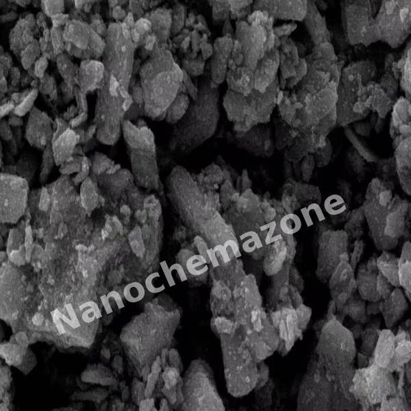
Applications of Sputtering Targets;
Film deposition is accomplished using sputtering targets. A technique for sputtering thin films is called "deposition made by sputter targets," which entails eroding material from a "target" source onto a "substrate" like a silicon wafer.
Etching of the target is done using semiconductor sputtering targets. When selectivity is not an issue and a high degree of etching anisotropy is required, sputter etching is the method of choice.
By removing the target material through etching, sputter targets are also utilized for investigation.
In secondary ion spectroscopy (SIMS), one example is when the target material is sputtered at a steady pace. When the target shatters,
Mass spectrometry measures the concentration and identity of sputtered atoms. The target material's composition may be ascertained and even very low concentrations of contaminants can be found with the aid of the sputtering target.
There is also an application area for sputtering targets in space. One type of space weathering that alters the chemical and physical characteristics of airless worlds like the Moon and asteroids is sputtering.
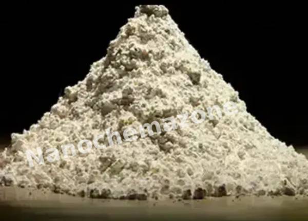
Group 15 of the periodic table contains antimony (Sb), which shares an atomic number of 51 with bismuth and arsenic. It gleams with a metallic sheen. bluish-white in color. Despite not having the same reputation as a poison, antimony shares many of the same chemical characteristics as arsenic. Its average natural abundance in the earth's crust is 0.2 to 0.5 parts per million. Antimony sputtering targets can be utilized to create fire-retardant coatings since antimony has excellent fire retardance properties. Antimony sputtering targets can also be utilized for optoelectronic devices such as solar cells, laser diodes, photodiodes, and LEDs.