Copper Oxide (CuO) Nanopowder/Nanoparticles Water Dispersion, Size: 20-50 nm, 22 wt%

Price range: $81.00 through $635.00
Select options This product has multiple variants. The options may be chosen on the product page
30 ml/72 € 60 ml/120 € 120 ml/202 € 500 ml/559 €   
Please contact us for quotes on larger quantities !!!

Copper Oxide (CuO) Nanopowder/Nanoparticles Water Dispersion

Size: 20-50 nm, 22 wt%

Barium Titanate (BaTiO3) Sputtering Targets, Purity: 99.99%, Size: 2”, Thickness: 0.125”

$634.00

Product 

Barium Titanate (BaTiO3) Sputtering Targets, Purity: 99.99%, Size: 2'', Thickness: 0.125''

CAS No.

 12047‑27‑7

Appearance

Powder

Purity

≥99%,  ≥99.9%,  ≥95%

(Other purities are also available)

APS

1 – 5 µm (Size Can be customized), Ask for other available size ranges.

Ingredient

N/A

Molecular Weight

233.19 g/mol

Melting Point

~1625 °C

Boiling Point

N/A

Density

 ~6.02 g/cm³

Product Codes

NCZ-2464K

Tantalum Oxide (Ta2O5) Sputtering Targets, Purity: 99.99%, Size: 3”, Thickness: 0.125”

$634.00

Product 

Tantalum Oxide (Ta2O5) Sputtering Targets, Purity: 99.99%, Size: 3'', Thickness: 0.125''

CAS No.

1314-61-0

Appearance

Powder

Purity

≥99%,  ≥99.9%,  ≥95%

(Other purities are also available)

APS

N/A  (Size Can be customized), Ask for other available size ranges.

Ingredient

N/A

Molecular Weight

 441.89 g/mol

Melting Point

 ~1872 °C

Boiling Point

N/A

Density

~8.2 g/cm³

Product Codes

NCZ-1652K

Indium Zinc Oxide/IZO (InZnO) Sputtering Targets, indium, Purity: 99.99%, Size: 2”, Thickness: 0.125”

$634.00

Applications of Sputtering Targets;

Film deposition is accomplished using sputtering targets. A technique for sputtering thin films is called "deposition made by sputter targets," which entails eroding material from a "target" source onto a "substrate" like a silicon wafer. Etching of the target is done using semiconductor sputtering targets. When selectivity is not an issue and a high degree of etching anisotropy is required, sputter etching is the method of choice. By removing the target material through etching, sputter targets are also utilized for investigation. In secondary ion spectroscopy (SIMS), one example is when the target material is sputtered at a steady pace. Mass spectrometry is used to quantify the concentration and identity of spewed atoms as the target is sputtered.

The target material's composition may be ascertained and even very low concentrations of contaminants can be found with the aid of the sputtering target.

There is also an application area for sputtering targets in space. One type of space weathering that alters the chemical and physical characteristics of airless worlds like the Moon and asteroids is sputtering.

Boron Carbide (B4C) Sputtering Targets, indium, Purity: 99.5%, Size: 2”, Thickness: 0.125”

$634.00

Applications of Sputtering Targets;

Film deposition is accomplished using sputtering targets. A technique for sputtering thin films is called "deposition made by sputter targets," which entails eroding material from a "target" source onto a "substrate" like a silicon wafer. Etching of the target is done using semiconductor sputtering targets. When selectivity is not an issue and a high degree of etching anisotropy is required, sputter etching is the method of choice. By removing the target material through etching, sputter targets are also utilized for investigation. In secondary ion spectroscopy (SIMS), one example is when the target material is sputtered at a steady pace. Mass spectrometry is used to quantify the concentration and identity of spewed atoms as the target is sputtered.

The target material's composition may be ascertained and even very low concentrations of contaminants can be found with the aid of the sputtering target.

There is also an application area for sputtering targets in space. One type of space weathering that alters the chemical and physical characteristics of airless worlds like the Moon and asteroids is sputtering.

Cadmium (Cd) Micron Powder, Purity: 99.99 %, Size: 200 mesh, Irregular

Price range: $28.00 through $634.00
Select options This product has multiple variants. The options may be chosen on the product page
25 grams/25 € 100 grams/66 € 500 grams/175 € 1000 grams/560 €
Please contact us for quotes on larger quantities !!!

Cadmium (Cd) Micron Powder

Purity: 99.99 %, Size: 200 mesh, Irregular

Technical Properties:

PURITY

99.99 %

PARTICLE SIZE

200 Mesh

CAS

7440-43-9

DENSITY

8.65 g/cm³

BOILING POINT

765 °C

MELTING POINT

320.9 °C

MOHS HARDNESS @ 20ºC

2

COEFF. OF EXPANSION @ 20ºC

29.8 x 10 ⁻⁶

ELECTRIC RESISTIVITY

6.83 microhm-cm

CRYSTAL STRUCTURE

Hexagonal

FORM  

Powder

APPLICATIONS

Alloys, Customer Manufacturing, Industrial- general


Bismuth Telluride (Bi2Te3) Sputtering Targets, Purity: 99.999%, Size: 1”, Thickness: 0.125”

$633.00

Product 

Bismuth Telluride (Bi2Te3) Sputtering Targets, Purity: 99.999%, Size: 1'', Thickness: 0.125''

CAS No.

 1304-82-1

Appearance

Powder

Purity

≥99%,  ≥99.9%,  ≥95%

(Other purities are also available)

APS

 N/A (Size Can be customized), Ask for other available size ranges.

Ingredient

N/A

Molecular Weight

800.55 g/mol

Melting Point

~585 °C

Boiling Point

~987 °C (sublimes)

Density

 ~7.7 g/cm³

Product Codes

NCZ-2403K

Bismuth Telluride (Bi2Te3) Sputtering Targets, Purity: 99.999%, Size: 1”, Thickness: 0.250”

$633.00

Product 

Bismuth Telluride (Bi2Te3) Sputtering Targets, Purity: 99.999%, Size: 1'', Thickness: 0.250''

CAS No.

 1304-82-1

Appearance

Powder

Purity

≥99%,  ≥99.9%,  ≥95%

(Other purities are also available)

APS

 N/A (Size Can be customized), Ask for other available size ranges.

Ingredient

N/A

Molecular Weight

800.55 g/mol

Melting Point

~585 °C

Boiling Point

~987 °C (sublimes)

Density

 ~7.7 g/cm³

Product Codes

NCZ-2402K

Molybdenum Disilicide (MoSi2) Sputtering Targets, Purity: 99.95%, Size: 3”, Thickness: 0.125”

$633.00

Applications of Sputtering Targets;

Film deposition is accomplished using sputtering targets. A technique for sputtering thin films is called "deposition made by sputter targets," which entails eroding material from a "target" source onto a "substrate" like a silicon wafer. Etching of the target is done using semiconductor sputtering targets. When selectivity is not an issue and a high degree of etching anisotropy is required, sputter etching is the method of choice. By removing the target material through etching, sputter targets are also utilized for investigation. In secondary ion spectroscopy (SIMS), one example is when the target material is sputtered at a steady pace. Mass spectrometry is used to quantify the concentration and identity of spewed atoms as the target is sputtered.

By helping of the sputtering target, the composition of the target material may be evaluated and even extremely tiny amounts of contaminants are recognized.

There is also an application area for sputtering targets in space. One type of space weathering that alters the chemical and physical characteristics of airless worlds like the Moon and asteroids is sputtering.

Titanium Dioxide (TiO2) Nanopowder/Nanoparticles Dispersion in 2-Propanol, Size: 12 nm, Anatase, 22 wt%

Price range: $119.00 through $633.00
Select options This product has multiple variants. The options may be chosen on the product page
Titanium Dioxide (TiO2) Nanopowder/Nanoparticles Dispersion in 2-Propanol Size: 12 nm, Anatase, 22 wt%

Polyglutamic acid(PGA, Agriculture grade) (539522)

Price range: $466.00 through $632.00
Select options This product has multiple variants. The options may be chosen on the product page
Polyglutamic acid(PGA, Agriculture grade) (539522) Agricultural polyglutamic acid is a green environmentally-friendly fertilizer synergist that can increase fertilizer utilization from 30-35% to 40-50%, with an average utilization increase of 7-12% in nitrogen fertilizer, an average increase of 10-25% in crop yield and even 60% in some crops. Major strengths are listed as follows. 1. Rich nutrients that improve utilization; 2. Long-term slow release; 3. Improve soil physical and chemical properties; 4. Improve crop quality and yield; 5. Environmental friendly. Specifications
Appearance Yellow to off white powder with a few agglomeration
Assay(HPLC) ≥25%
Loss on drying(105°C, 2h) ≤6%
pH(10g/L, 25°C) 4.0-8.5
Heavy metals(Pb, mg/kg) ≤20
    Product Codes- NCZ-2676K

Polyglutamic acid(PGA, Cosmetic grade) (439522)

Price range: $466.00 through $632.00
Select options This product has multiple variants. The options may be chosen on the product page
Polyglutamic acid(PGA, Cosmetic grade) (439522)
Synonym  Natto Gum, Sodium polyglutamate, γ-PGA Na, PGA, γ-PGA, γ-Polyglutamic acid Cas No  25513-46-6 Specifications
 
Appearance White to off white granular or powder, no agglomeration
Assay(HPLC) ≥92%
Loss on drying(105°C, 2h) ≤8%
Molecular wt(Da) 100,000-2,000,000
pH(10g/L, water solution, 25°C) 5.0-7.5
Transmittance(5g/L, water solution, 400nm) ≥95%
Heavy metals(Pb, mg/kg) ≤10
Total plate count(CFU/g) ≤100
  Product Codes- NCZ-2675K

Antimony Telluride (Sb2Te3) Sputtering Targets, Purity: 99.999%, Size: 1”, Thickness: 0.125”

$632.00

Product 

Antimony Telluride (Sb2Te3) Sputtering Targets, Purity: 99.999%, Size: 1'', Thickness: 0.125''

CAS No.

12068-69-8

Appearance

Powder

Purity

≥99%,  ≥99.9%,  ≥95%

(Other purities are also available)

APS

N/A (Size Can be customized), Ask for other available size ranges.

Ingredient

N/A

Molecular Weight

626.32 g/mol

Melting Point

620 °C

Boiling Point

N/A

Density

 6.50 g/cm³

Product Codes

NCZ-2500K

Cobalt Iron Boron (Co-Fe-B) Sputtering Targets, Purity: 99.9%, Size: 3”, Thickness: 0.250”

$632.00

Product 

Cobalt Iron Boron (Co-Fe-B) Sputtering Targets, Purity: 99.9%, Size: 3'', Thickness: 0.250''

CAS No.

N/A

Appearance

Powder

Purity

≥99%,  ≥99.9%,  ≥95%

(Other purities are also available)

APS

 N/A (Size Can be customized), Ask for other available size ranges.

Ingredient

N/A

Molecular Weight

 ≈ 125.59 g/mol

Melting Point

N/A

Boiling Point

N/A

Density

N/A

Product Codes

NCZ-2275K

Tantalum Oxide (Ta2O5) Sputtering Targets, Purity: 99.99%, Size: 4”, Thickness: 0.125”

$632.00

Product 

Tantalum Oxide (Ta2O5) Sputtering Targets, Purity: 99.99%, Size: 4'', Thickness: 0.125''

CAS No.

1314-61-0

Appearance

Powder

Purity

≥99%,  ≥99.9%,  ≥95%

(Other purities are also available)

APS

N/A  (Size Can be customized), Ask for other available size ranges.

Ingredient

N/A

Molecular Weight

 441.89 g/mol

Melting Point

 ~1872 °C

Boiling Point

N/A

Density

~8.2 g/cm³

Product Codes

NCZ-1649K

Zinc Oxide (ZnO) with Alumina Sputtering Targets, Purity: 99.99%, Size: 4”, Thickness: 0.250”

$632.00

Applications of Sputtering Targets;

Film deposition is accomplished using sputtering targets. A technique for sputtering thin films is called "deposition made by sputter targets," which entails eroding material from a "target" source onto a "substrate" like a silicon wafer. Etching of the target is done using semiconductor sputtering targets. When selectivity is not an issue and a high degree of etching anisotropy is required, sputter etching is the method of choice. By removing the target material through etching, sputter targets are also utilized for investigation. In secondary ion spectroscopy (SIMS), one example is when the target material is sputtered at a steady pace. Mass spectrometry is used to quantify the concentration and identity of spewed atoms as the target is sputtered.

The target material's composition may be ascertained and even very low concentrations of contaminants can be found with the aid of the sputtering target.

There is also an application area for sputtering targets in space. One type of space weathering that alters the chemical and physical characteristics of airless worlds like the Moon and asteroids is sputtering.

Tin Oxide (SnO2) Sputtering Targets, Purity: 99.99%, Size: 4”, Thickness: 0.125”

$631.00

Product 

Tin Oxide (SnO2) Sputtering Targets, Purity: 99.99%, Size: 4'', Thickness: 0.125''

CAS No.

18282-10-5

Appearance

Powder

Purity

≥99%,  ≥99.9%,  ≥95%

(Other purities are also available)

APS

N/A  (Size Can be customized), Ask for other available size ranges.

Ingredient

N/A

Molecular Weight

150.71 g/mol

Melting Point

~1630 °C

Boiling Point

~1800–1900 °C

Density

~6.95 g/cm³

Product Codes

NCZ-1626K

Lithium Nickel Cobalt Oxide (LiNi(1-x)CoxO2) Sputtering Targets, Purity: 99.9%, Size: 2”, Thickness: 0.250”

$631.00

Applications of Sputtering Targets;

Film deposition is accomplished using sputtering targets. A technique for sputtering thin films is called "deposition made by sputter targets," which entails eroding material from a "target" source onto a "substrate" like a silicon wafer. Etching of the target is done using semiconductor sputtering targets. When selectivity is not an issue and a high degree of etching anisotropy is required, sputter etching is the method of choice. By removing the target material through etching, sputter targets are also utilized for investigation. In secondary ion spectroscopy (SIMS), one example is when the target material is sputtered at a steady pace. Mass spectrometry is used to quantify the concentration and identity of spewed atoms as the target is sputtered.

By helping of the sputtering target, the composition of the target material may be evaluated and even extremely tiny amounts of contaminants are recognized.

There is also an application area for sputtering targets in space. One type of space weathering that alters the chemical and physical characteristics of airless worlds like the Moon and asteroids is sputtering.

Formula LiCoO2 represents the chemical compound lithium cobalt oxide. A crystalline solid that is dark blue or bluish-gray in color, lithium cobalt oxide is frequently utilized in the positive electrodes of lithium-ion batteries.

Carbon Nanotube (CNT) Nanoribbon Water Dispersion, 1 mg/mL

Price range: $54.00 through $631.00
Select options This product has multiple variants. The options may be chosen on the product page
Technical Properties: Purity:   > 95 wt% (carbon nanotubes) Outside diameter: 20-30 nm Inside diameter: 5-10 nm Length: 10-30 um SSA: > 110 m2/g

(-OH) Functionalized Short Length Multi Walled Carbon Nanotubes, Purity: > 96%, Outside Diameter: 4-16 nm

Price range: $47.00 through $631.00
Select options This product has multiple variants. The options may be chosen on the product page

Applications:

Multi Walled Carbon Nanotubes have a variety of potential applications in different fields. These applications include medicine, mechanics, electric-electronics, chemicals, energy and others. It can be applied in, 1-drug delivery, 2-biosensors, 3-CNT composites, 4-catalysis, 5-nanoprobes, 6-hydrogen storage, 7-lithium batteries, 8-gas-discharge tubes, 9-flat panel displays, 10-supercapacitors, 11-transistors, 12-solar cells, 13-photoluminescence, 14-templates

Silicon Oxide Nanoparticles / Nanopowder (SiO2, 99.8%, 5-15 nm, surface modified, hydrophobic & oleophilic, dispersible)

Price range: $93.00 through $630.00
Select options This product has multiple variants. The options may be chosen on the product page
$93/25g
$247/100g
$348/500g
$630/kg

Product 

Silicon Oxide Nanoparticles / Nanopowder (SiO2, 99.8%, 5-15 nm, surface modified, hydrophobic & oleophilic, dispersible)

CAS No.

7631-86-9

Appearance

Powder

Purity

≥99%,  ≥99.9%,  ≥95%

(Other purities are also available)

APS

5-15 nm (Size Can be customized), Ask for other available size ranges.

Ingredient

N/A

Molecular Weight

60.08 g/mol

Melting Point

~1,710 °C (core SiO₂)

Boiling Point

~2,230 °C

Density

~2.2 g/cm³

Product Codes

NCZ-1172K

Barium Titanate (BaTiO3) Sputtering Targets, Purity: 99.99%, Size: 3”, Thickness: 0.125”

$630.00

Applications of Sputtering Targets;

Film deposition is accomplished using sputtering targets. A technique for sputtering thin films is called "deposition made by sputter targets," which entails eroding material from a "target" source onto a "substrate" like a silicon wafer. Etching of the target is done using semiconductor sputtering targets. When selectivity is not an issue and a high degree of etching anisotropy is required, sputter etching is the method of choice. By removing the target material through etching, sputter targets are also utilized for investigation. In secondary ion spectroscopy (SIMS), one example is when the target material is sputtered at a steady pace. Mass spectrometry is used to quantify the concentration and identity of spewed atoms as the target is sputtered. With the sputtering target's assistance, the

It is possible to identify the target material and even detect incredibly tiny impurity amounts.

There is also an application area for sputtering targets in space. One type of space weathering that alters the chemical and physical characteristics of airless worlds like the Moon and asteroids is sputtering.

Formulated as BaTiO3, barium titanate is an inorganic substance. When formed as big crystals, barium titanate is clear and has a white powdery appearance. It is a ferroelectric ceramic material with piezoelectric and photorefractive characteristics. Titanate of barium sputtering Agents have various applications. For instance, barium titanate films, which are produced by sputtering targets, can be employed in particular electronic ceramics. Barium titanate can be utilized in the building of electrical devices such as sensors, capacitors, and detectors.

Barium Titanate (BaTiO3) Sputtering Targets, Purity: 99.99%, Size: 3”, Thickness: 0.125”

$630.00

Applications of Sputtering Targets;

Film deposition is accomplished using sputtering targets. A technique for sputtering thin films is called "deposition made by sputter targets," which entails eroding material from a "target" source onto a "substrate" like a silicon wafer. Etching of the target is done using semiconductor sputtering targets. When selectivity is not an issue and a high degree of etching anisotropy is required, sputter etching is the method of choice. By removing the target material through etching, sputter targets are also utilized for investigation. In secondary ion spectroscopy (SIMS), one example is when the target material is sputtered at a steady pace. Mass spectrometry is used to quantify the concentration and identity of spewed atoms as the target is sputtered. With the sputtering target's assistance, the It is possible to identify the target material and even detect incredibly tiny impurity amounts. There is also an application area for sputtering targets in space. One type of space weathering that alters the chemical and physical characteristics of airless worlds like the Moon and asteroids is sputtering. Formulated as BaTiO3, barium titanate is an inorganic substance. When formed as big crystals, barium titanate is clear and has a white powdery appearance. It is a ferroelectric ceramic material with piezoelectric and photorefractive characteristics. The applications for barium titanate sputtering agents are numerous. For instance, barium titanate films, which are produced by sputtering targets, can be employed in particular electronic ceramics. Regarding the construction of electrical equipment such

Aluminum Oxide (Al2O3) Sputtering Targets, Purity: 99.999%, Size: 3”, Thickness: 0.125”

$630.00

Applications of Sputtering Targets;

Film deposition is accomplished using sputtering targets. A technique for sputtering thin films is called "deposition made by sputter targets," which entails eroding material from a "target" source onto a "substrate" like a silicon wafer. Etching of the target is done using semiconductor sputtering targets. When selectivity is not an issue and a high degree of etching anisotropy is required, sputter etching is the method of choice. By removing the target material through etching, sputter targets are also utilized for investigation. In secondary ion spectroscopy (SIMS), one example is when the target material is sputtered at a steady pace. When the target shatters,

Mass spectrometry measures the concentration and identity of sputtered atoms. The target material's composition may be ascertained and even very low concentrations of contaminants can be found with the aid of the sputtering target.

There is also an application area for sputtering targets in space. One type of space weathering that alters the chemical and physical characteristics of airless worlds like the Moon and asteroids is sputtering.

With the chemical formula Al2O3, aluminum oxide is a compound made of aluminum and oxygen.

Tin (Sn) Sputtering Targets, Purity: 99.99%, Size: 4”, Thickness: 0.250”

$629.00

Product 

Tin (Sn) Sputtering Targets, Purity: 99.99%, Size: 4'', Thickness: 0.250''

CAS No.

7440-31-5

Appearance

Powder

Purity

≥99%,  ≥99.9%,  ≥95%

(Other purities are also available)

APS

N/A  (Size Can be customized), Ask for other available size ranges.

Ingredient

N/A

Molecular Weight

118.71 g/mol

Melting Point

231.93 °C

Boiling Point

2602 °C

Density

~7.31 g/cm³

Product Codes

NCZ-1638K

Tungsten (W) Sputtering Target

Price range: $63.00 through $629.00
Select options This product has multiple variants. The options may be chosen on the product page

Product 

Tungsten (W) Sputtering Target

CAS No.

7440-33-7

Appearance

Powder

Purity

≥99%,  ≥99.9%,  ≥95%

(Other purities are also available)

APS

 NA (Size Can be customized), Ask for other available size ranges.

Ingredient

N/A

Molecular Weight

183.84 g/mol

Melting Point

3,422 °C

Boiling Point

5,555 °C

Density

19.25 g/cm³

Product Codes

NCZ-1307K

Aluminum Nitride (AlN) Sputtering Targets, Purity: 99.8%, Size: 2”, Thickness: 0.125”

$629.00

 Applications of Sputtering Targets;

Film deposition is accomplished using sputtering targets. A technique for sputtering thin films is called "deposition made by sputter targets," which entails eroding material from a "target" source onto a "substrate" like a silicon wafer. Etching of the target is done using semiconductor sputtering targets. When selectivity is not an issue and a high degree of etching anisotropy is required, sputter etching is the method of choice. By removing the target material through etching, sputter targets are also utilized for investigation. In secondary ion spectroscopy (SIMS), one example is when the target material is sputtered at a steady pace. Mass spectrometry is used to quantify the concentration and identity of spewed atoms as the target is sputtered. With the sputtering target's assistance, the

It is possible to identify the target material's composition and even detect incredibly low impurity quantities.

There is also an application area for sputtering targets in space. One type of space weathering that alters the chemical and physical characteristics of airless worlds like the Moon and asteroids is sputtering.

The chemical compound aluminum nitride has the formula AlN. The combination of mechanical, chemical, and physical properties of aluminum nitride is exceptional. Superior aluminum nitride films have found application in a wide range of sensors and devices, including optoelectronic and optical ones. High refractive index (~2.0), low absorption, and a broad band gap (~6.2 eV) are important characteristics for optical and optoelectronic applications.

Aluminum Nitride (AlN) Sputtering Targets, Purity: 99.8%, Size: 2”, Thickness: 0.125”

$629.00

 Applications of Sputtering Targets;

  • Sputtering targets is used for film deposition. The deposition made by sputter targets is a method of depositing thin films by sputtering that involves eroding material from a "target" source onto a "substrate" such as  a silicon wafer.
  • Semiconductor sputtering targets is used to etch the target. Sputter etching is chosen in cases where a high degree of etching anisotropy is needed and selectivity is not a concern.
  • Sputter targets is also used for analysis by etching away the target material.
One of the example occurs in secondary ion spectroscopy (SIMS), where the target sample is sputtered at a constant rate. As the target is sputtered, the concentration and identity of sputtered atoms are measured using mass spectrometry. By helping of the sputtering target, the composition of the target material can be determined and even extremely low concentrations of impurities are detected. Sputtering target has also application area in space. Sputtering is one of the forms of space weathering, a process that changes the physical and chemical properties of airless bodies, such as asteroids and the Moon. 
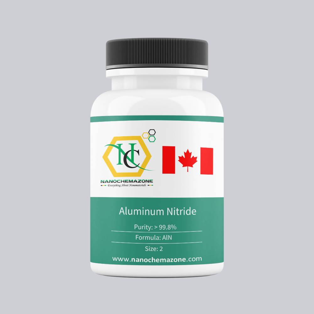
Aluminum nitride is a chemical compound with the formula of AlN.Aluminum nitride has excellent combination of physical, chemical, and mechanical properties. High-quality films of aluminum nitride have been used in various devices and sensors including the optical and optoelectronic devices. As far as the optical and optoelectronic applications are concerned, wide band gap (~6.2 eV) along with high-refractive index (~2.0) and low-absorption coefficient (<10−3) makes AlN a very attractive material for these applications. In addition to this, thermal and chemical stability of AlN films make it suitable for applications in difficult environment. Today, AlN films/coatings have been grown by several methods which include pulsed laser deposition, reactive molecular beam epitaxy, vacuum arc/cathodic arc deposition, DC/RF reactive sputtering, ion beam sputtering, metal-organic chemical vapor deposition (MOCVD), and miscellaneous other techniques. Due to simplicity, reproducibility, ease of scaling up, and lower cost, magnetron sputtering is one of the common methods for growing AlN films for various applications. Properties of AlN films depend upon the crystal structure, crystal orientation, microstructure, and chemical composition, which in turn depend upon the deposition conditions such as sputtering power, pulse frequency, duty cycle, growth temperature, nitrogen/argon flow ratio, and sputtering gas pressure. AlN sputtering targets give good result with the method of reactive DC magnetron sputtering system.

Magnesium (Mg) Sputtering Targets, Purity: 99.98%, Size: 8”, Thickness: 0.250”

$628.00

Product 

Magnesium (Mg) Sputtering Targets, Purity: 99.98%, Size: 8'', Thickness: 0.250''

CAS No.

7439-95-4

Appearance

Powder

Purity

≥99%,  ≥99.9%,  ≥95%

(Other purities are also available)

APS

 N/A (Size Can be customized), Ask for other available size ranges.

Ingredient

N/A

Molecular Weight

 24.305 g/mol

Melting Point

 650 °C

Boiling Point

 1,090 °C

Density

1.738 g/cm³

Product Codes

NCZ-1987K

Tungsten Disulfide (WS2) Sputtering Targets, Purity: 99.9%, Size: 4”, Thickness: 0.250”

$628.00

Product 

Tungsten Disulfide (WS2) Sputtering Targets, Purity: 99.9%, Size: 4'', Thickness: 0.250''

CAS No.

 12138-09-9

Appearance

Powder

Purity

≥99%,  ≥99.9%,  ≥95%

(Other purities are also available)

APS

N/A  (Size Can be customized), Ask for other available size ranges.

Ingredient

N/A

Molecular Weight

247.97 g/mol

Melting Point

~1,250 °C

Boiling Point

N/A

Density

~7.5 g/cm³

Product Codes

NCZ-1579K

Tungsten Disulfide (WS2) Sputtering Targets, indium, Purity: 99.9%, Size: 2”, Thickness: 0.125”

$628.00

Product 

Tungsten Disulfide (WS2) Sputtering Targets, indium, Purity: 99.9%, Size: 2'', Thickness: 0.125''

CAS No.

12138-09-9

Appearance

Powder

Purity

≥99%,  ≥99.9%,  ≥95%

(Other purities are also available)

APS

N/A  (Size Can be customized), Ask for other available size ranges.

Ingredient

N/A

Molecular Weight

247.97 g/mol

Melting Point

~1,250 °C

Boiling Point

N/A

Density

~7.5 g/cm³

Product Codes

NCZ-1575K

Titanium Dioxide (TiO2) Sputtering Targets, Purity: 99.9%, Size: 4”, Thickness: 0.250”, Grey to Black

$628.00

Product 

Titanium Dioxide (TiO2) Sputtering Targets, Purity: 99.9%, Size: 4'', Thickness: 0.250'', Grey to Black

CAS No.

13463‑67‑7

Appearance

Powder

Purity

≥99%,  ≥99.9%,  ≥95%

(Other purities are also available)

APS

TiO₂ (black granules) (Size Can be customized), Ask for other available size ranges.

Ingredient

N/A

Molecular Weight

79.94 g/mol

Melting Point

~1,843 °C

Boiling Point

~2,972 °C

Density

~4.23 g/cm³

Product Codes

NCZ-1430K

3N5 (99.95%) Niobium Oxide (Nb2O5) Pieces (3-12mm) Evaporation Materials

Price range: $276.00 through $628.00
Select options This product has multiple variants. The options may be chosen on the product page
Product 3N5 (99.95%) Niobium Oxide (Nb2O5) Pieces (3-12mm) Evaporation Materials
CAS No. 1313-96-8
Appearance White, Crystalline Solid, Grey-Black
Purity ≥99%,  ≥99.9%,  ≥95%(Other purities are also available)
APS 3-12mm (Size Can be customized),  Ask for other available size range.
Ingredient Nb2O5
Molecular Weight 265.81 g/mol
Melting Point 1,485 °C
Boiling Point N/A
Density 4.6 g/cm3
Product Codes NCZ-145E
 

Zinc Sulfide (ZnS) Sputtering Targets, Purity: 99.99%, Size: 3”, Thickness: 0.125”

$628.00

Applications of Sputtering Targets;

Film deposition is accomplished using sputtering targets. A technique for sputtering thin films is called "deposition made by sputter targets," which entails eroding material from a "target" source onto a "substrate" like a silicon wafer. Etching of the target is done using semiconductor sputtering targets. When selectivity is not an issue and a high degree of etching anisotropy is required, sputter etching is the method of choice. By removing the target material through etching, sputter targets are also utilized for investigation. In secondary ion spectroscopy (SIMS), one example is when the target material is sputtered at a steady pace. Mass spectrometry is used to quantify the concentration and identity of spewed atoms as the target is sputtered.

The target material's composition may be ascertained and even very low concentrations of contaminants can be found with the aid of the sputtering target.

There is also an application area for sputtering targets in space. One type of space weathering that alters the chemical and physical characteristics of airless worlds like the Moon and asteroids is sputtering.

Calcium Manganate (CaMnO3) Sputtering Targets, Purity: 99.9%, Size: 4”, Thickness: 0.125”

$627.00

Product 

Calcium Manganate (CaMnO3) Sputtering Targets, Purity: 99.9%, Size: 4'', Thickness: 0.125''

CAS No.

12058-85-6

Appearance

Powder

Purity

≥99%,  ≥99.9%,  ≥95%

(Other purities are also available)

APS

 N/A (Size Can be customized), Ask for other available size ranges.

Ingredient

N/A

Molecular Weight

157.87 g/mol

Melting Point

 Approx. 1400 °C (decomposes)

Boiling Point

N/A

Density

 ~4.7 g/cm³

Product Codes

NCZ-2357K

Molybdenum Disulfide (MoS2) Sputtering Targets, Purity: 99.9%, Size: 3”, Thickness: 0.125”

$627.00

Product 

Molybdenum Disulfide (MoS2) Sputtering Targets, Purity: 99.9%, Size: 3'', Thickness: 0.125''

CAS No.

 1317-33-5

Appearance

Powder

Purity

≥99%,  ≥99.9%,  ≥95%

(Other purities are also available)

APS

 N/A (Size Can be customized), Ask for other available size ranges.

Ingredient

N/A

Molecular Weight

 160.07 g/mol

Melting Point

 ~1185 °C

Boiling Point

 ~4500 °C

Density

 ~5.06 g/cm³

Product Codes

NCZ-1915K

Selenium (Se) Sputtering Targets, Purity: 99.999%, Size: 4”, Thickness: 0.250”

$627.00

Product 

Selenium (Se) Sputtering Targets, Purity: 99.999%, Size: 4'', Thickness: 0.250''

CAS No.

7782-49-2

Appearance

Powder

Purity

≥99%,  ≥99.9%,  ≥95%

(Other purities are also available)

APS

N/A  (Size Can be customized), Ask for other available size ranges.

Ingredient

N/A

Molecular Weight

 78.96 g/mol

Melting Point

 221 °C

Boiling Point

 685 °C

Density

 4.81 g/cm³

Product Codes

NCZ-1768K

99.5% Niobium (Nb) Micron Powder (3um), 1kg

$627.00
Product 99.5% Niobium (Nb) Micron Powder (3um), 1kg
CAS No. 7440-03-1
Appearance Gray
Purity ≥99%,  ≥99.9%,  ≥95%(Other purities are also available)
APS 3um (Size Can be customized),  Ask for other available size range.
Ingredient Nb
Molecular Weight N/A
Melting Point 4742 °C
Boiling Point 2468 °C
Density N/A
Product Codes NCZ-220I

Zinc Oxide (ZnO) Sputtering Targets, Purity: 99.9%, Size: 3”, Thickness: 0.125”

$627.00

Product 

Zinc Oxide (ZnO) Sputtering Targets, Purity: 99.9%, Size: 3'', Thickness: 0.125''

CAS No.

1314‑13‑2

Appearance

Powder

Purity

≥99%,  ≥99.9%,  ≥95%

(Other purities are also available)

APS

ZnO (black granules) (Size Can be customized), Ask for other available size ranges.

Ingredient

N/A

Molecular Weight

81.38 g/mol

Melting Point

~1975 °C

Boiling Point

~2360 °C

Density

 ~5.61 g/cm³

Product Codes

NCZ-1449K

Zinc Oxide (ZnO) Sputtering Targets, Purity: 99.999%, Size: 3”, Thickness: 0.125”

$627.00

Product 

Zinc Oxide (ZnO) Sputtering Targets, Purity: 99.999%, Size: 3'', Thickness: 0.125''

CAS No.

1314‑13‑2

Appearance

Powder

Purity

≥99%,  ≥99.9%,  ≥95%

(Other purities are also available)

APS

ZnO (black granules) (Size Can be customized), Ask for other available size ranges.

Ingredient

N/A

Molecular Weight

81.38 g/mol

Melting Point

~1975 °C

Boiling Point

~2360 °C

Density

 ~5.61 g/cm³

Product Codes

NCZ-1448K

Nickel/Iron (Ni/Fe 81/19 wt.%) Pellets Evaporation Materials

Price range: $165.00 through $627.00
Select options This product has multiple variants. The options may be chosen on the product page
Product Nickel/Iron (Ni/Fe 81/19 wt.%) Pellets Evaporation Materials
CAS No. N/A
Appearance Silver-gray to dark gray
Purity ≥99%,  ≥99.9%,  ≥95%(Other purities are also available)
APS N/A
Ingredient Ni/Fe
Molecular Weight 265.81 g/mol
Melting Point N/A
Boiling Point N/A
Density 8.7 g/cm3
Product Codes NCZ-147E

3N5 (99.95%) Molybdenum Trioxide (MoO3) Pellets (1-3mm) Evaporation Materials

Price range: $229.00 through $627.00
Select options This product has multiple variants. The options may be chosen on the product page
Product 3N5 (99.95%) Molybdenum Trioxide (MoO3) Pellets (1-3mm) Evaporation Materials
CAS No. 1313-27-5
Appearance White or Pale Yellow, Crystalline Solid 
Purity ≥99%,  ≥99.9%,  ≥95%(Other purities are also available)
APS 1-3mm (Size Can be customized),  Ask for other available size range.
Ingredient MoO3
Molecular Weight 143.95 g/mol
Melting Point 795 °C
Boiling Point N/A
Density 4.69 g/cm³
Product Codes NCZ-132E

Silicon Nitride (Si3N4) Sputtering Targets, Purity: 99.5%, Size: 3”, Thickness: 0.250”, Dark Gray to Black

$627.00

Applications of Sputtering Targets;

Film deposition is accomplished using sputtering targets. A technique for sputtering thin films is called "deposition made by sputter targets," which entails eroding material from a "target" source onto a "substrate" like a silicon wafer. Etching of the target is done using semiconductor sputtering targets. When selectivity is not an issue and a high degree of etching anisotropy is required, sputter etching is the method of choice. By removing the target material through etching, sputter targets are also utilized for investigation. In secondary ion spectroscopy (SIMS), one example is when the target material is sputtered at a steady pace. Mass spectrometry is used to quantify the concentration and identity of spewed atoms as the target is sputtered. The target material's composition may be ascertained and even very low concentrations of contaminants can be found with the aid of the sputtering target. There is also an application area for sputtering targets in space. One type of space weathering that alters the chemical and physical characteristics of airless worlds like the Moon and asteroids is sputtering.

Carbon Nanotubes Doped with 32 wt% Silicon (Si) and 32 wt% Graphene Nanopowder/Nanoparticles

Price range: $108.00 through $627.00
Select options This product has multiple variants. The options may be chosen on the product page
Applications:  

Carbon NanoTubes doped with Graphene nanoplatelets and Silicon nanopowders demonstrate significant improvements in electrical and mechanical properties. Hardness, tensile strength, specific strength, and elastic modulus are examples of such enhancements. Because of these advancements, these materials are now widely used in a variety of applications. Some of these programs. 1 -drug delivery, 2 biosensors, 3 CNT composites 4-catalysis, 5-nanoprobes, Storage of 6-hydrogen, 7-lithium-ion batteries, There are 8 gas discharge tubes and 9 - flat panel displays, 10-supercapacitors, 11- transistors , 12-solar cells, 13-photoluminescence ,14-templates.


Ytterbium Oxide (Yb2O3) Sputtering Targets, Purity: 99.99%, Size: 3”, Thickness: 0.125”

$626.00

Product 

Ytterbium Oxide (Yb2O3) Sputtering Targets, Purity: 99.99%, Size: 3'', Thickness: 0.125''

CAS No.

1314-37-0

Appearance

Powder

Purity

≥99%,  ≥99.9%,  ≥95%

(Other purities are also available)

APS

N/A  (Size Can be customized), Ask for other available size ranges.

Ingredient

N/A

Molecular Weight

394.08 g/mol

Melting Point

2346 °C

Boiling Point

4127 °C

Density

 9.17 g/cm³

Product Codes

NCZ-1525K

Carbon Nanotube-Carbon Black Prepared by Electrostatic Adsorption, CNTs: 34.4 wt%, Carbon Black: 65.6 wt%

Price range: $147.00 through $626.00
Select options This product has multiple variants. The options may be chosen on the product page
5 grams/134 € 25 grams/253 € 100 grams/568 €                                    
Please contact us for quotes on larger quantities !!!

Carbon Nanotube-Black Carbon Prepared by Electrostatic Adsorption

CNTs: 34.4 wt%, Carbon Black: 65.6 wt%

Technical Properties:

Carbon Nanotubes > 95 wt%
Purity >50
Outside Diameter (nm) 5.0-15.0
Inside Diameter (nm) 5.0-20.0
Length (μm) CVD
Color black
Super Conductive Black Carbon Nanoparticles 
Average Particle Size (nm) 50-100
Shape spherical
CNTs 33.3 wt%, Carbon Black 66.7 wt%
Specific Surface Area (m2/g) 560
Volume Resistivity (Ω.cm) <1
Volume Resistivity Content Relationship
CNTs Content wt%  0.00  25.00  33.30  60.00
Volume Resistivity (Ω·cm)  0.2150  0.1544  0.1332  0.1198

Applications:

Super conductive black carbon nanoparticles surface is usually negatively charged. Carbon nanotubes are treated with cationic surfactant (Cetyl trimethyl ammonium bromide). Carbon nanotubes and black carbon self assemble to form a uniform stable complex. The complex shows high strength and conductivity which makes it suitable for processing into conductive plastics, conductive sheets, and films.  

Manganese (Mn) Sputtering Targets, Purity: 99.95%, Size: 8”, Thickness: 0.250”

$625.00

Product 

Manganese (Mn) Sputtering Targets, Purity: 99.95%, Size: 8'', Thickness: 0.250''

CAS No.

 7439-96-5

Appearance

Powder

Purity

≥99%,  ≥99.9%,  ≥95%

(Other purities are also available)

APS

 N/A (Size Can be customized), Ask for other available size ranges.

Ingredient

N/A

Molecular Weight

54.93804 g/mol

Melting Point

 1,246 °C

Boiling Point

 2,061 °C

Density

 7.21 g/cm³

Product Codes

NCZ-1945K

Tin (Sn) Sputtering Targets, Purity: 99.99%, Size: 6”, Thickness: 0.250”

$625.00

Product 

Tin (Sn) Sputtering Targets, Purity: 99.99%, Size: 6'', Thickness: 0.250''

CAS No.

7440-31-5

Appearance

Powder

Purity

≥99%,  ≥99.9%,  ≥95%

(Other purities are also available)

APS

N/A  (Size Can be customized), Ask for other available size ranges.

Ingredient

N/A

Molecular Weight

118.71 g/mol

Melting Point

231.93 °C

Boiling Point

2602 °C

Density

~7.31 g/cm³

Product Codes

NCZ-1636K

Tin Oxide (SnO2) Sputtering Targets, Purity: 99.99%, Size: 1”, Thickness: 0.125”

$625.00

Product 

Tin Oxide (SnO2) Sputtering Targets, Purity: 99.99%, Size: 1'', Thickness: 0.125''

CAS No.

18282-10-5

Appearance

Powder

Purity

≥99%,  ≥99.9%,  ≥95%

(Other purities are also available)

APS

N/A  (Size Can be customized), Ask for other available size ranges.

Ingredient

N/A

Molecular Weight

150.71 g/mol

Melting Point

~1630 °C

Boiling Point

~1800–1900 °C

Density

~6.95 g/cm³

Product Codes

NCZ-1632K

Cadmium (Cd) Sputtering Target

Price range: $221.00 through $625.00
Select options This product has multiple variants. The options may be chosen on the product page

Product 

Cadmium (Cd) Sputtering Target

CAS No.

7440-43-9

Appearance

Powder

Purity

≥99%,  ≥99.9%,  ≥95%

(Other purities are also available)

APS

 NA (Size Can be customized), Ask for other available size ranges.

Ingredient

N/A

Molecular Weight

112.41 g/mol

Melting Point

321.07 °C

Boiling Point

767 °C

Density

8.65 g/cm³

Product Codes

NCZ-1286K

Zinc Oxide Nano-dispersion in water

Price range: $205.00 through $625.00
Select options This product has multiple variants. The options may be chosen on the product page
$625/500g
$205/100g

Product 

Zinc Oxide Nano-dispersion in water

CAS No.

1314-13-2

Appearance

Powder

Purity

≥99%,  ≥99.9%,  ≥95%

(Other purities are also available)

APS

~10–50 nm(Size Can be customized), Ask for other available size ranges.

Ingredient

N/A

Molecular Weight

81.38 g/mol

Melting Point

~1,975 °C

Boiling Point

~2,360 °C

Density

 ~5.61 g/cm³

Product Codes

NCZ-1221K

Prime CZ-Si Wafer, Size: 2”, Orientation: (111), Boron Doped, Resistivity: 1-20 (ohm.cm), 2-Side Polished, Thickness: 500 ± 25 μm

Price range: $38.00 through $625.00
Select options This product has multiple variants. The options may be chosen on the product page
Prime CZ-Si Wafer Size: 2”, Orientation: (111), Boron Doped, 2-Side Polished Technical Properties: Quality Prime Materials CZ-Si Size (inch) 2”

Aluminum Oxide Nanoparticles

Price range: $75.00 through $625.00
Select options This product has multiple variants. The options may be chosen on the product page

Aluminum Oxide Nanoparticles

MF: Al2O3, alpha
Chemical Name: Aluminum Oxide
Purity: > 99.99%
APS: 200 nm
Form: Nanopowder
Product Number: #NCZ2201
CAS Number 1344-28-1

Aluminum Oxide Nanoparticles

Note: We can supply different size products of microparticles and Nanoparticles Size range powder according to the client’s requirements.

Barium Sulfate (BaSO4) Nanoparticles

Price range: $75.00 through $625.00
Select options This product has multiple variants. The options may be chosen on the product page

Barium Sulfate Nanoparticles

MF: BaSO4
Chemical Name: Barium Sulfate
Purity: > 99.99%
APS: 200-500 nm (Size Customization possible)
Form: Nanopowder
Product Number: #NCZ701
CAS Number 7727-43-7

Barium Sulfate Nanoparticles

Note: We can supply different size products of microparticles and Nanoparticles Size range powder according to the client’s requirements.

Aluminium Hydroxide nanoparticles

Price range: $75.00 through $625.00
Select options This product has multiple variants. The options may be chosen on the product page

Aluminium Hydroxide nanoparticles

MF: Al(OH)3

Chemical Name:

Aluminium Hydroxide 

Purity: > 99.99%
APS: 20 nm (Size Customization possible)
Form: Nanopowder
Product Number: #NCZ301
CAS Number 21645-51-2

Aluminium Hydroxide nanoparticles

Note: We can supply different size products of microparticles and Nanoparticles Size range powder according to the client’s requirements.

Tungsten Titanium (TiW) Sputtering Targets, Purity: 99.99%, Size: 4”, Thickness: 0.125”

$624.00

Applications of Sputtering Targets;

Film deposition is accomplished using sputtering targets. A technique for sputtering thin films is called "deposition made by sputter targets," which entails eroding material from a "target" source onto a "substrate" like a silicon wafer. Etching of the target is done using semiconductor sputtering targets. When selectivity is not an issue and a high degree of etching anisotropy is required, sputter etching is the method of choice. By removing the target material through etching, sputter targets are also utilized for investigation. In secondary ion spectroscopy (SIMS), one example is when the target material is sputtered at a steady pace. Mass spectrometry is used to quantify the concentration and identity of spewed atoms as the target is sputtered.

The target material's composition may be ascertained and even very low concentrations of contaminants can be found with the aid of the sputtering target.

There is also an application area for sputtering targets in space. One type of space weathering that alters the chemical and physical characteristics of airless worlds like the Moon and asteroids is sputtering.

Titanium Dioxide (TiO2) Sputtering Targets, indium, Purity: 99.9%, Size: 2”, Thickness: 0.125”, Grey to Black

$624.00

Applications of Sputtering Targets;

Film deposition is accomplished using sputtering targets. A technique for sputtering thin films is called "deposition made by sputter targets," which entails eroding material from a "target" source onto a "substrate" like a silicon wafer. Etching of the target is done using semiconductor sputtering targets. When selectivity is not an issue and a high degree of etching anisotropy is required, sputter etching is the method of choice. By removing the target material through etching, sputter targets are also utilized for investigation. In secondary ion spectroscopy (SIMS), one example is when the target material is sputtered at a steady pace. Mass spectrometry is used to quantify the concentration and identity of spewed atoms as the target is sputtered.

The target material's composition may be ascertained and even very low concentrations of contaminants can be found with the aid of the sputtering target.

There is also an application area for sputtering targets in space. One type of space weathering that alters the chemical and physical characteristics of airless worlds like the Moon and asteroids is sputtering.

Silicon Carbide (SiC) Sputtering Targets, Purity: 99.5%, Size: 4”, Thickness: 0.250”

$624.00

Applications of Sputtering Targets;

Film deposition is accomplished using sputtering targets. A technique for sputtering thin films is called "deposition made by sputter targets," which entails eroding material from a "target" source onto a "substrate" like a silicon wafer. Etching of the target is done using semiconductor sputtering targets. When selectivity is not an issue and a high degree of etching anisotropy is required, sputter etching is the method of choice. By removing the target material through etching, sputter targets are also utilized for investigation. In secondary ion spectroscopy (SIMS), one example is when the target material is sputtered at a steady pace. Mass spectrometry is used to quantify the concentration and identity of spewed atoms as the target is sputtered.

The target material's composition may be ascertained and even very low concentrations of contaminants can be found with the aid of the sputtering target.

There is also an application area for sputtering targets in space. One type of space weathering that alters the chemical and physical characteristics of airless worlds like the Moon and asteroids is sputtering.

Silicon Carbide (SiC) Sputtering Targets, Purity: 99.5%, Size: 3”, Thickness: 0.250”

$624.00

Applications of Sputtering Targets;

Film deposition is accomplished using sputtering targets. A technique for sputtering thin films is called "deposition made by sputter targets," which entails eroding material from a "target" source onto a "substrate" like a silicon wafer. Etching of the target is done using semiconductor sputtering targets. When selectivity is not an issue and a high degree of etching anisotropy is required, sputter etching is the method of choice. By removing the target material through etching, sputter targets are also utilized for investigation. In secondary ion spectroscopy (SIMS), one example is when the target material is sputtered at a steady pace. Mass spectrometry is used to quantify the concentration and identity of spewed atoms as the target is sputtered.

The target material's composition may be ascertained and even very low concentrations of contaminants can be found with the aid of the sputtering target.

There is also an application area for sputtering targets in space. One type of space weathering that alters the chemical and physical characteristics of airless worlds like the Moon and asteroids is sputtering.

Carbon Nanotube-Carbon Black Prepared by Electrostatic Adsorption, CNTs: 34.4 wt%, Carbon Black: 65.6 wt%

Price range: $149.00 through $624.00
Select options This product has multiple variants. The options may be chosen on the product page
Carbon Nanotube-Black Carbon Prepared by Electrostatic Adsorption CNTs: 34.4 wt%, Carbon Black: 65.6 wt% Technical Properties: Carbon Nanotubes > 95