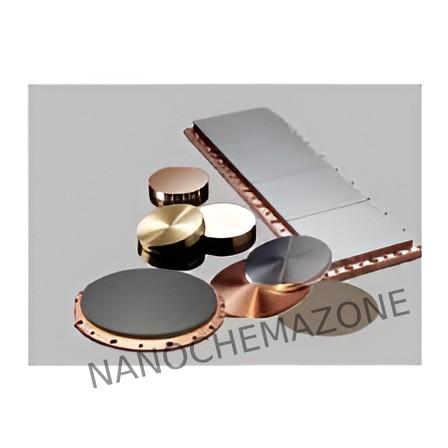
Applications of Sputtering Targets;
Film deposition is accomplished using sputtering targets. A technique for sputtering thin films is called "deposition made by sputter targets," which entails eroding material from a "target" source onto a "substrate" like a silicon wafer.
Etching of the target is done using semiconductor sputtering targets. When selectivity is not an issue and a high degree of etching anisotropy is required, sputter etching is the method of choice.
By removing the target material through etching, sputter targets are also utilized for investigation.
In secondary ion spectroscopy (SIMS), one example is when the target material is sputtered at a steady pace. When the target shatters,
Mass spectrometry measures the concentration and identity of sputtered atoms. The target material's composition may be ascertained and even very low concentrations of contaminants can be found with the aid of the sputtering target.
There is also an application area for sputtering targets in space. One type of space weathering that alters the chemical and physical characteristics of airless worlds like the Moon and asteroids is sputtering.
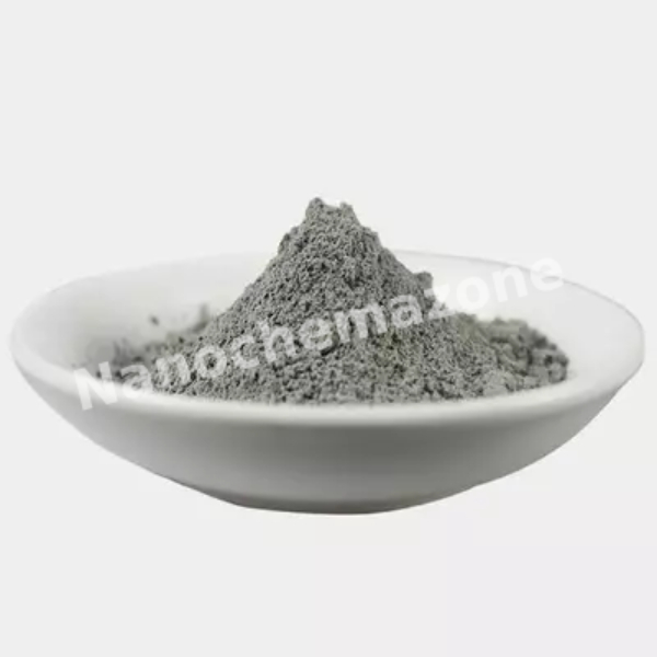
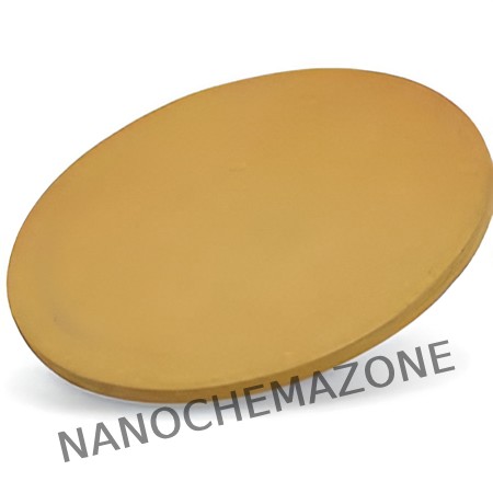
With the chemical formula Al2O3, aluminum oxide is a compound made of aluminum and oxygen. Because of its high melting point, Al2O3 is useful as a refractory material and as an abrasive due to its hardness, as well as for the production of aluminum metal. Thin coatings of aluminum oxide that can
be acquired using aluminum oxide Because of their exceptional qualities, including great resistance to abrasion and corrosion, transparency, mechanical strength and hardness, as well as insulating and optical qualities, sputtering targets are widely employed in a variety of mechanical, optical, and microelectronic applications. All of these characteristics of aluminum oxide film are dependent on several sputtering system parameters, including sputtering rate, target-to-substrate distance, reactive gas pressures, etc.