Prime CZ-Si Wafer, Size: 6”, Orientation: (100), Boron Doped, Resistivity: 1-10 (ohm.cm), 1-Side Polished, Thickness: 525±25um

Price range: $53.00 through $1,050.00
Select options This product has multiple variants. The options may be chosen on the product page
Prime CZ-Si Wafer Size: 6”, Orientation: (100), Boron Doped, 1-Side Polished, Thickness: 525±25um Technical Properties: Quality Prime Materials CZ-Si Size (inch)

Prime CZ-Si Wafer, Size: 2”, Orientation: (100), Boron Doped, Resistivity: 1-10 (ohm.cm), 2-Side Polished, Thickness: 500 ± 25 μm

Price range: $53.00 through $640.00
Select options This product has multiple variants. The options may be chosen on the product page
Prime CZ-Si Wafer Size: 2”, Orientation: (100), Boron Doped, 2-Side Polished Technical Properties: Quality Prime Materials CZ-Si Size (inch) 2”

Reduced Graphene Oxide (rGO),Purity: 99%, S.A: 15.62 m2/g, 2-5 layers

Price range: $53.00 through $985.00
Select options This product has multiple variants. The options may be chosen on the product page
1 gram: 53 € 5 grams: 105 € 25 grams: 434 € 100 grams: 985 €  Contact us for tailored quotes on larger quantities & experience exceptional solutions from

Calcium Carbonate Nanoparticles / Nanopowder(CaCO3, 97.5+%, 15~40nm)

Price range: $53.00 through $84.00
Select options This product has multiple variants. The options may be chosen on the product page
$53/100g
$84/500g

Product 

Calcium Carbonate Nanoparticles / Nanopowder(CaCO3, 97.5+%, 15~40nm)

CAS No.

471-34-1

Appearance

Powder

Purity

≥99%,  ≥99.9%,  ≥95%

(Other purities are also available)

APS

15~40nm(Size Can be customized), Ask for other available size ranges.

Ingredient

N/A

Molecular Weight

100.09 g/mol

Melting Point

 Decomposes at ~825 °C

Boiling Point

N/A

Density

~2.71 g/cm³

Product Codes

NCZ-1108K

Zirconium Oxide Micron Powder (ZrO2, 99.9%, 1~3um)

Price range: $53.00 through $181.00
Select options This product has multiple variants. The options may be chosen on the product page
$53/100g
$117/500g
$181/kg

Product 

Zirconium Oxide Micron Powder (ZrO2, 99.9%, 1~3um)

CAS No.

1314-23-4

Appearance

Powder

Purity

≥99%,  ≥99.9%,  ≥95%

(Other purities are also available)

APS

~10–50 nm(Size Can be customized), Ask for other available size ranges.

Ingredient

N/A

Molecular Weight

123.22 g/mol

Melting Point

~2,715 °C

Boiling Point

~4,300 °C

Density

~5.68 g/cm³

Product Codes

NCZ-1224K

Short Length Multi Walled Carbon Nanotubes, Purity: > 96%, Outside Diameter: 18-28 nm

Price range: $54.00 through $1,449.00
Select options This product has multiple variants. The options may be chosen on the product page

Applications:

Multi Walled Carbon Nanotubes have a variety of potential applications in different fields. These applications include medicine, mechanics, electric-electronics, chemicals, energy and others. It can be applied in, 1-drug delivery, 2-biosensors, 3-CNT composites, 4-catalysis, 5-nanoprobes, 6-hydrogen storage, 7-lithium batteries, 8-gas-discharge tubes, 9-flat panel displays, 10-supercapacitors, 11-transistors, 12-solar cells, 13-photoluminescence, 14-templates

Reduced Graphene Oxide (rGO), S.A: 1562 m2/g, 2-5 layers

Price range: $54.00 through $1,014.00
Select options This product has multiple variants. The options may be chosen on the product page
Reduced Graphene Oxide (rGO) is derived by deoxygenation of graphene oxide via chemical, thermal, electrochemical process or through IR or UV irradiation to get a powder form. Reduced graphene oxide is the most suitable solution for bulk material applications such as energy storage thanks to be manufactured easily in large quantities with desired quantity level. For applications requiring the highest uniformity in size, we offer high purity of Reduced Graphene Oxide (rGO) with lowest prices.

Cubic Boron Nitride Nanopowder, Cubic, Size: <200 nm Purity: 99.9%

Price range: $54.00 through $5,434.00
Select options This product has multiple variants. The options may be chosen on the product page
gram:48 € 5 gram:138 € 25 gram:395€ 100 gram:785 € 500 gram:2975€ 1000 gram:4790€
Please contact us for quotes on larger quantities !!!
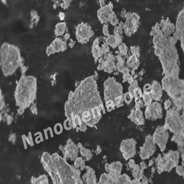
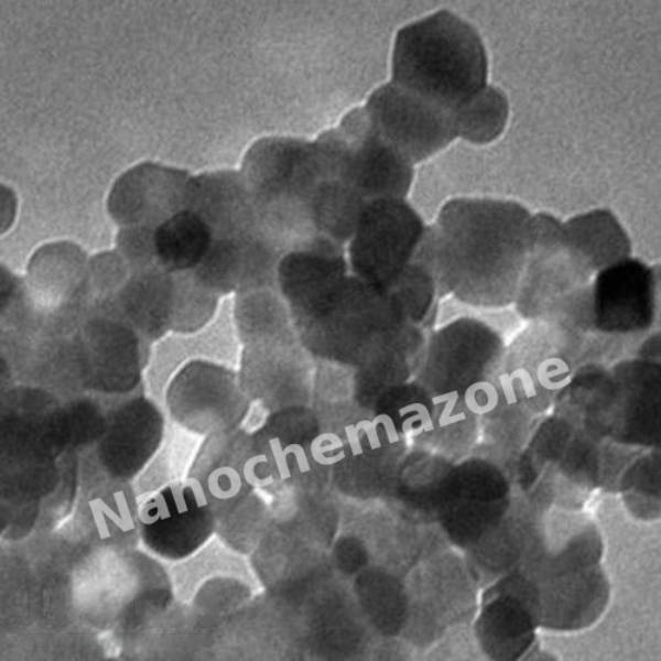
Cubic Boron Nitride (BN) Nanopowder Purity: 99.9% Size: 200 nm Cubic boron nitride has a crystal structure analogous to that of diamond. Consistent with diamond being less stable than graphite, the cubic form is less stable than the hexagonal form, but the conversion rate between the two is negligible at room temperature, as it is for diamond. The cubic form has the sphalerite crystal structure, the same as that of diamond, and is also called β-BN or c-BN.

PREPARATION OF CUBIC BORON NITRIDE

Synthesis of c-BN uses same methods as that of diamond: Cubic boron nitride is produced by treating hexagonal boron nitride at high pressure and temperature, much as synthetic diamond is produced from graphite. Direct conversion of hexagonal boron nitride to the cubic form has been observed at pressures between 5 and 18 GPa and temperatures between 1730 and 3230 °C, that is similar parameters as for direct graphite-diamond conversion.  The addition of a small amount of boron oxide can lower the required pressure to 4–7 GPa and temperature to 1500 °C. As in diamond synthesis, to further reduce the conversion pressures and temperatures, a catalyst is added, such as lithium, potassium, or magnesium, their nitrides, their fluoronitrides, water with ammonium compounds, or hydrazine.Other industrial synthesis methods, again borrowed from diamond growth, use crystal growth in a temperature gradient, or explosive shock wave. The shock wave method is used to produce material called heterodiamond, a superhard compound of boron, carbon, and nitrogen. Low-pressure deposition of thin films of cubic boron nitride is possible. As in diamond growth, the major problem is to suppress the growth of hexagonal phases (h-BN or graphite, respectively). Whereas in diamond growth this is achieved by adding hydrogen gas, boron trifluoride is used for c-BN. Ion beam deposition, plasma-enhanced chemical vapor deposition, pulsed laser deposition, reactive sputtering, and other physical vapor deposition methods are used as well. Applications of CBN Cubic boron nitride (CBN or c-BN) is widely used as an abrasive. Its usefulness arises from its insolubility in iron, nickel, and related alloys at high temperatures, whereas diamond is soluble in these metals. Polycrystalline c-BN (PCBN) abrasives are therefore used for machining steel, whereas diamond abrasives are preferred for aluminum alloys, ceramics, and stone. When in contact with oxygen at high temperatures, BN forms a passivation layer of boron oxide. Boron nitride binds well with metals, due to formation of interlayers of metal borides or nitrides. Materials with cubic boron nitride crystals are often used in the tool bits of cutting tools. For grinding applications, softer binders, e.g. resin, porous ceramics, and soft metals, are used. Ceramic binders can be used as well. Commercial products are known under names "Borazon" (by Diamond Innovations), and "Elbor" or "Cubonite" (by Russian vendors). Contrary to diamond, large c-BN pellets can be produced in a simple process (called sintering) of annealing c-BN powders in nitrogen flow at temperatures slightly below the BN decomposition temperature. This ability of c-BN and h-BN powders to fuse allows cheap production of large BN parts. Similar to diamond, the combination in c-BN of highest thermal conductivity and electrical resistivity is ideal for heat spreaders. As cubic boron nitride consists of light atoms and is very robust chemically and mechanically, it is one of the popular materials for X-ray membranes: low mass results in small X-ray absorption, and good mechanical properties allow usage of thin membranes, thus further reducing the absorption.

Cerium (Ce) Micron Powder, Purity: 99.5 %, Size: 325 mesh

Price range: $54.00 through $3,376.00
Select options This product has multiple variants. The options may be chosen on the product page
1 gram/48 € 5 grams/194 € 25 grams/870 € 100 grams/2980 €
Please contact us for quotes on larger quantities !!!

Cerium (Ce) Micron Powder

Purity: 99.5 %, Size: 325 mesh

Technical Properties:

PURITY

 99.5 %

PARTICLE SIZE

325 mesh

MELTING POINT 

799 °C

BOILING POINT 

3426 °C

DENSITY

6.657 gm/cc

FORM  

Powder

ELECTRIC RESISTIVITY

75.0 microhm-cm @ 25 °C


Applications:

Cerium is the most abundant element of the rare earth elements. It is found in minerals sallanite, rhabdophane, hydroxylbastnasite, bastnasite, monazite, synchysite, and zircon. It is ductile and it oxidizes very quickly at room temperature. Cerium nanoparticles are graded as highly flammable and harmful. Cerium powder is applied as polishing agent in glass polishing. It is very efficient glass polishing agents. It is used for precision optical polishing because of its strong oxidizing properties. It is also used to remove ultrafine diesel particle emissions like carbon. It is used in steel manufacturing to remove unwanted trace elements such as lead and antimony and to remove free oxygen and sulfur. Cerium powder has also applications in fuel cells functions for example it is used in the electrolyte of solid oxide fuel cells. 

Molybdenum (Mo) Micron Powder, Purity: 99.99 %, Size: 1 µm

Price range: $54.00 through $445.00
Select options This product has multiple variants. The options may be chosen on the product page
25 grams/48 € 100 grams/98 € 500 grams/295 € 1000 grams/395 €  
Please contact us for quotes on larger quantities !!!

Molybdenum (Mo) Micron Powder

Purity: 99.99 %, Size: 1 µm

Technical Properties:

PURITY

99.99 %

PARTICLE SIZE

1 µm

CAS

7439-98-7

MELTING POINT

2610 °C

BOILING POINT

5560 °C

CRYSTAL STRUCTURE

Cubic, Body Centered

DENSITY                                         8.2 g/cm³
COEFF. OF EXPANSION @ 20ºC

5.1 x 10⁻⁶

ELECTRIC RESISTIVITY

5.17 microhm-cm

FORM  

Powder

APPLICATIONS

Aerospace Alloys Electronics Metal Injection Molding


Prime CZ-Si Wafer, Size: 6”, Orientation: (111), Boron Doped, Resistivity: 1-2 (ohm.cm), 1-Side Polished, Thickness: 675 ± 15 μm

Price range: $54.00 through $1,035.00
Select options This product has multiple variants. The options may be chosen on the product page
1 piece/49 € 5 pieces/210 € 25 pieces/925 € Please contact us for quotes on larger quantities !!!

Prime CZ-Si Wafer

Size: 6”, Orientation: (111), Boron Doped, 1-Side Polished, Thickness: 675 ± 15 μm

Technical Properties:

Quality Prime
Materials CZ-Si
Size (inch) 6”
Orientation (111)
Coating  
Thickness (μm) 675 ± 15
Doping Boron
Resistivity (ohm.cm) 1-2
Polished One Side
Silicon is one of the most common elements on earths crust. Main usage of Silicon wafers is electronics and technology. Silicon wafers have very flat and mirror like surfaces. It is produced by Czochralski method to obtain the highest purity. Depending on the usage area, silicon wafers can be doped with different materials to tailor its purity accordingly. The amount and type of dopants highly affect the electronic properties. Galium, indium, boron and nitrogen are some of the dopants that can be used in production process. Silicon wafers are used in semiconductors, microchips, integrated circuits, smartphones, computers etc. Silicon is the key platform for semiconductor gadgets. A wafer is just but a thin slice of the semiconductor material that acts as a substratum for microelectronic devices fitted in and above the wafer.

Prime CZ-Si Wafer, Size: 4”, Orientation: (100), Boron Doped, Resistivity: 0.001 – 0.005 (ohm.cm), 2- Polished, Thickness: 200 ± 10 μm

Price range: $54.00 through $1,007.00
Select options This product has multiple variants. The options may be chosen on the product page
1 piece/49 € 5 pieces/195 € 25 pieces/900 € Please contact us for quotes on larger quantities !!!

Prime CZ-Si Wafer

Size: 4”, Orientation: (100), Boron Doped, 2- Polished

Technical Properties:

Quality Prime
Materials CZ-Si
Size (inch) 4”
Orientation (100)
Coating  
Thickness (μm) 200 ± 10 μm
Doping Boron
Resistivity (ohm.cm) 0.001 - 0.005
Polished Double Side
Silicon is one of the most common elements on earths crust. Main usage of Silicon wafers is electronics and technology. Silicon wafers have very flat and mirror like surfaces. It is produced by Czochralski method to obtain the highest purity. Depending on the usage area, silicon wafers can be doped with different materials to tailor its purity accordingly. The amount and type of dopants highly affect the electronic properties. Galium, indium, boron and nitrogen are some of the dopants that can be used in production process. Silicon wafers are used in semiconductors, microchips, integrated circuits, smartphones, computers etc. Silicon is the key platform for semiconductor gadgets. A wafer is just but a thin slice of the semiconductor material that acts as a substratum for microelectronic devices fitted in and above the wafer.

Fused Silica Wafer, Size: 4”, 2-Side Polished, Thickness: 1000 ± 25 μm

Price range: $54.00 through $1,054.00
Select options This product has multiple variants. The options may be chosen on the product page
1 piece/49 € 5 pieces/210 € 25 pieces/950 € Please contact us for quotes on larger quantities !!!

Fused Silica Wafer

Size: 4”, 2-Side Polished, Thickness: 1000 ± 25 μm

Technical Properties:

Quality Prime
Materials Fused Silica
Size(inch) 4”
Orientation
Coating
Thickness (μm) 1000 ± 25
Doping
Resistivity(ohm.cm)
Polished Double Side
Fused silica – also referred as fused quartz- is an amorphous phase of silica. Compared to borosilicate wafers, fused silica has no additives. Is almost chemically inactive. Has a very high thermal resistance. Has an improved optical transmission in deep UV (ultraviolet). Silica dust particles are deposited on the substrate first, solidification of these molten particles creates a pure fused phase on the surface with the help of flame hydrolysis.

Silicon Dioxide (SiO2) Nanopowder/Nanoparticles Dispersion in Ethylene Glycol, Size: 22 nm, Amorphous, 15 wt%

Price range: $54.00 through $1,055.00
Select options This product has multiple variants. The options may be chosen on the product page
Silicon Dioxide (SiO2) Nanopowder/Nanoparticles Dispersion in Ethylene Glycol Size: 22 nm, Amorphous, 15 wt%

Silicon Dioxide (SiO2) Nanopowder/Nanoparticles Dispersion in 1, 2-Propanediol, Size: 22 nm, Amorphous, 15 wt%

Price range: $54.00 through $1,008.00
Select options This product has multiple variants. The options may be chosen on the product page
30 ml/54 € 60 ml/119 € 120 ml/231 € 500 ml/656 € 1000 ml/1008 €         Please contact us for quotes on larger

Silicon Dioxide (SiO2) Nanopowder/Nanoparticles Dispersion in Water, Amorphous, Size: 28 nm, 26 wt%

Price range: $54.00 through $300.00
Select options This product has multiple variants. The options may be chosen on the product page
Silicon Dioxide (SiO2) Nanopowder/Nanoparticles Dispersion in Water Amorphous, Size: 28 nm, 26 wt%

Carbon Nanotube (CNT) Nanoribbon Water Dispersion, 1 mg/mL

Price range: $54.00 through $631.00
Select options This product has multiple variants. The options may be chosen on the product page
Technical Properties: Purity:   > 95 wt% (carbon nanotubes) Outside diameter: 20-30 nm Inside diameter: 5-10 nm Length: 10-30 um SSA: > 110 m2/g

Gold (Au) Nanopowder/Nanoparticles Dispersion, Purity: 99.99%, Size: 20-30 nm, 172 ppm

Price range: $54.00 through $451.00
Select options This product has multiple variants. The options may be chosen on the product page
Gold (Au) Nanopowder/Nanoparticles Dispersion Purity: 99.99%, Size: 20-30 nm, 172 ppm Technical Properties: Au Nanoparticle Purity (%) 99,99 Au Concentration

Carbon Nanotube (CNT) Nanoribbon Water Dispersion, 1 mg/mL

Price range: $55.00 through $649.00
Select options This product has multiple variants. The options may be chosen on the product page
Manufacturing Method:Ribbon is produced by chemical oxidation and longitudinal opening using strong oxidizing agents.  

Graphitized Multi Walled Carbon Nanotubes, Purity: > 99.99%, Outside Diameter: 28-48 nm

Price range: $55.00 through $622.00
Select options This product has multiple variants. The options may be chosen on the product page

Applications:

Multi Walled Carbon Nanotubes have a variety of potential applications in different fields. These applications include medicine, mechanics, electric-electronics, chemicals, energy and others. It can be applied in, 1-drug delivery, 2-biosensors, 3-CNT composites, 4-catalysis, 5-nanoprobes, 6-hydrogen storage, 7-lithium batteries, 8-gas-discharge tubes, 9-flat panel displays, 10-supercapacitors, 11-transistors, 12-solar cells, 13-photoluminescence, 14-templates

Short Length Multi Walled Carbon Nanotubes, Purity: > 96%, Outside Diameter: 28-48 nm

Price range: $55.00 through $1,781.00
Select options This product has multiple variants. The options may be chosen on the product page

Applications:

Multi Walled Carbon Nanotubes have a variety of potential applications in different fields. These applications include medicine, mechanics, electric-electronics, chemicals, energy and others. It can be applied in, 1-drug delivery, 2-biosensors, 3-CNT composites, 4-catalysis, 5-nanoprobes, 6-hydrogen storage, 7-lithium batteries, 8-gas-discharge tubes, 9-flat panel displays, 10-supercapacitors, 11-transistors, 12-solar cells, 13-photoluminescence, 14-templates

(-COOH) Functionalized Short Length Multi Walled Carbon Nanotubes, Purity: > 96%, Outside Diameter: 28-48 nm

Price range: $55.00 through $1,802.00
Select options This product has multiple variants. The options may be chosen on the product page

Applications:

Multi Walled Carbon Nanotubes have a variety of potential applications in different fields. These applications include medicine, mechanics, electric-electronics, chemicals, energy and others. It can be applied in, 1-drug delivery, 2-biosensors, 3-CNT composites, 4-catalysis, 5-nanoprobes, 6-hydrogen storage, 7-lithium batteries, 8-gas-discharge tubes, 9-flat panel displays, 10-supercapacitors, 11-transistors, 12-solar cells, 13-photoluminescence, 14-templates

Yttrium Fluoride (YF3) Nanopowder, Purity: 99.9%, APS: < 50 nm

Price range: $55.00 through $562.00
Select options This product has multiple variants. The options may be chosen on the product page
25 grams: 49 €   100 grams: 97 €   500 grams: 298 €  1000 grams:  495 € Please contact us for quotes on larger quantities !!!    Yttrium Fluoride (YF3) Nanopowder Purity: 99.9%, APS: < 50 nm CAS #: 13709-49-4 Linear Formula: YF3 CERTIFICATE OF ANALYSIS Purity                       99.9 % Ti                            ≤50ppm Fe                           ≤50ppm Al                            ≤10ppm K                             ≤30ppm   SEM IMAGE OF THE PRODUCT  

Yttrium Fluoride (YF3) Nanopowder, Purity: 99.9%, APS: < 50 nm

Price range: $55.00 through $561.00
Select options This product has multiple variants. The options may be chosen on the product page
25 grams: 49 €   100 grams: 97 €   500 grams: 298 €  1000 grams:  495 € Please contact us for quotes on larger quantities !!!    Yttrium Fluoride (YF3) Nanopowder Purity: 99.9%, APS: < 50 nm CAS #: 13709-49-4 Linear Formula: YF3 CERTIFICATE OF ANALYSIS Purity                       99.9 % Ti                            ≤50ppm Fe                           ≤50ppm Al                            ≤10ppm K                             ≤30ppm  

Prime CZ-Si Wafer, Size: 2”, Orientation: (111), Phosphor Doped, Resistivity: 1-10 (ohm.cm), 1-Side Polished, Thickness: 280 ± 15 μm

Price range: $55.00 through $660.00
Select options This product has multiple variants. The options may be chosen on the product page
1 piece/50 € 5 pieces/150 € 25 pieces/590 € Please contact us for quotes on larger quantities !!!

Prime CZ-Si Wafer

Size: 2”, Orientation: (111), Phosphor Doped, 1-Side Polished

Technical Properties:

Quality Prime
Materials CZ-Si
Size (inch) 2”
Orientation (111)
Coating
Thickness (μm) 280 ± 15
Doping Phosphor
Resistivity (ohm.cm) 1-10
Polished One Side
Silicon is one of the most common elements on earths crust. Main usage of Silicon wafers is electronics and technology. Silicon wafers have very flat and mirror like surfaces. It is produced by Czochralski method to obtain the highest purity. Depending on the usage area, silicon wafers can be doped with different materials to tailor its purity accordingly. The amount and type of dopants highly affect the electronic properties. Galium, indium, boron and nitrogen are some of the dopants that can be used in production process. Silicon wafers are used in semiconductors, microchips, integrated circuits, smartphones, computers etc. Silicon is the key platform for semiconductor gadgets. A wafer is just but a thin slice of the semiconductor material that acts as a substratum for microelectronic devices fitted in and above the wafer.

Nickel Tab with Adhesive Polymer Tape as Negative Terminal for Pouch Cell, Width: 4 mm

Price range: $55.00 through $212.00
Select options This product has multiple variants. The options may be chosen on the product page

Applications:

4 mm Wide Nickel Tabs for use as the Negative Terminal of Polymer Li-ion Batteries

Industrial Grade Multi Walled Carbon Nanotubes, Purity: > 92%, Outside Diameter: 48-78 nm

Price range: $55.00 through $349.00
Select options This product has multiple variants. The options may be chosen on the product page

Applications:

Multi Walled Carbon Nanotubes have a wide range of possible uses in several industries. These applications span a variety of fields, including energy, chemistry, mechanics, and electric-electronics. Drug delivery, biosensors, CNT composites, catalysis, nanoprobes, and hydrogen storage are just a few applications for it. 7, lithium-ion batteries, eight gas discharge tubes nine flat-panel screens, ten supercapacitors, and eleven transistors a dozen solar cells, 14 templates, 13 photoluminescence

(-OH) Functionalized Multi Walled Carbon Nanotubes, Purity: > 96%, Outside Diameter: 4-16 nm

Price range: $55.00 through $1,405.00
Select options This product has multiple variants. The options may be chosen on the product page

Applications:

Multi-walled carbon nanotubes have numerous potential uses in various industries. Medicine, mechanics, electric-electronics, chemistry, energy, and other fields are among these uses. Drug delivery, biosensors, CNT composites, catalysis, nanoprobes, hydrogen storage, flat panel displays, supercapacitors, transistors, solar cells, photoluminescence, and templates are just a few areas where it can be used.

Nickel Tab with Adhesive Polymer Tape as Negative Terminal for Pouch Cell, Width: 4 mm

Price range: $55.00 through $212.00
Select options This product has multiple variants. The options may be chosen on the product page

Applications:

4 mm Wide Nickel Tabs for use as the Negative Terminal of Polymer Li-ion Batteries

Silver Ag Nanoparticles/ Nanopowder (Ag, 99.95%, 100nm)

Price range: $55.00 through $390.00
Select options This product has multiple variants. The options may be chosen on the product page
$55/5g $95/10g $155/25g $390/100g  

Product 

Silver Ag Nanoparticles/ Nanopowder (Ag, 99.95%, 100nm)

CAS No.

24304-00-5

Appearance

Powder

Purity

≥99%,  ≥99.9%,  ≥95%

(Other purities are also available)

APS

50-100 nm, 1-5 µM, 10-53 µM  (Size Can be customized), Ask for other available size ranges.

Ingredient

AlN

Molecular Weight

40.982 g/mol

Melting Point

2200 °C

Boiling Point

2517 °C

Density

3.3 g/cm³

Product Codes

NCZ-1001K

Nickel Powder ( Ni, 99.9%, -325 mesh )

Price range: $55.00 through $245.00
Select options This product has multiple variants. The options may be chosen on the product page
$55/100g
$175/500g
$245/1kg

Product 

Nickel Powder ( Ni, 99.9%, -325 mesh )

CAS No.

7440-02-0

Appearance

Powder

Purity

≥99%,  ≥99.9%,  ≥95%

(Other purities are also available)

APS

-325 mesh (Size Can be customized), Ask for other available size ranges.

Ingredient

N/A

Molecular Weight

58.69 g/mol

Melting Point

1455 °C

Boiling Point

2913 °C

Density

8.90 g/cm³

Product Codes

NCZ-1058K

Boron Oxide Powder ( B2O3, 98%, -200mesh)

Price range: $55.00 through $165.00
Select options This product has multiple variants. The options may be chosen on the product page
$55/100g
$165/500g

Product 

Boron Oxide Powder ( B2O3, 98%, -200mesh)

CAS No.

1303-86-2

Appearance

Powder

Purity

≥99%,  ≥99.9%,  ≥95%

(Other purities are also available)

APS

-200mesh (Size Can be customized), Ask for other available size ranges.

Ingredient

N/A

Molecular Weight

69.62 g/mol

Melting Point

~450 °C

Boiling Point

~1,860 °C

Density

~2.46 g/cm³

Product Codes

NCZ-1102K

Calcium Carbonate Nanoparticles / nanopowder, surface modified for plastic, PE/PP

Price range: $55.00 through $107.00
Select options This product has multiple variants. The options may be chosen on the product page
$55/100g
$107/kg

Product 

Calcium Carbonate Nanoparticles / nanopowder, surface modified for plastic, PE/PP

CAS No.

471-34-1

Appearance

Powder

Purity

≥99%,  ≥99.9%,  ≥95%

(Other purities are also available)

APS

15-40nm(Size Can be customized), Ask for other available size ranges.

Ingredient

N/A

Molecular Weight

100.09 g/mol

Melting Point

 Decomposes at ~825 °C

Boiling Point

N/A

Density

~2.71 g/cm³

Product Codes

NCZ-1110K

Calcium Carbonate Nanoparticles / Nanopowder, surface modified for rubber

Price range: $55.00 through $107.00
Select options This product has multiple variants. The options may be chosen on the product page
$55/100g
$107/kg

Product 

Calcium Carbonate Nanoparticles / Nanopowder, surface modified for rubber

CAS No.

471-34-1

Appearance

Powder

Purity

≥99%,  ≥99.9%,  ≥95%

(Other purities are also available)

APS

15-40nm(Size Can be customized), Ask for other available size ranges.

Ingredient

N/A

Molecular Weight

100.09 g/mol

Melting Point

 Decomposes at ~825 °C

Boiling Point

N/A

Density

~2.71 g/cm³

Product Codes

NCZ-1113K

Calcium Carbonate Nanoparticles / Nanopowder, surface modified for adhesives ( 98.5%, 15~40nm)

Price range: $55.00 through $107.00
Select options This product has multiple variants. The options may be chosen on the product page
$55/100g
$107/kg

Product 

Calcium Carbonate Nanoparticles / Nanopowder, surface modified for adhesives ( 98.5%, 15~40nm)

CAS No.

471-34-1

Appearance

Powder

Purity

≥99%,  ≥99.9%,  ≥95%

(Other purities are also available)

APS

15~40nm(Size Can be customized), Ask for other available size ranges.

Ingredient

N/A

Molecular Weight

100.09 g/mol

Melting Point

 Decomposes at ~825 °C

Boiling Point

N/A

Density

~2.71 g/cm³

Product Codes

NCZ-1115K

Erbium Oxide Nanoparticles / Nanopowder ( Er2O3, 40~50nm)

Price range: $55.00 through $345.00
Select options This product has multiple variants. The options may be chosen on the product page
$55/25g
$120/100g
$345/500g

Product 

Erbium Oxide Nanoparticles / Nanopowder ( Er2O3, 40~50nm)

CAS No.

12061-16-4

Appearance

Powder

Purity

≥99%,  ≥99.9%,  ≥95%

(Other purities are also available)

APS

 40~50nm (Size Can be customized), Ask for other available size ranges.

Ingredient

N/A

Molecular Weight

382.52 g/mol

Melting Point

~2,340 °C

Boiling Point

~3,800 °C

Density

~8.64 g/cm³

Product Codes

NCZ-1130K

Cerium Oxide Nanopowder/ Nanoparticles (Nanoceria or CeO2, 10~30nm, 99.9%) (Copy)

Price range: $55.00 through $315.00
Select options This product has multiple variants. The options may be chosen on the product page
$55/25g
$115/100g
$205/500g
$315/kg

Product 

Cerium Oxide Nanopowder/ Nanoparticles (Nanoceria or CeO2, 10~30nm, 99.9%)

CAS No.

1306-38-3

Appearance

Powder

Purity

≥99%,  ≥99.9%,  ≥95%

(Other purities are also available)

APS

10~30nm (Size Can be customized), Ask for other available size ranges.

Ingredient

N/A

Molecular Weight

172.11 g/mol

Melting Point

~1,590 °C

Boiling Point

3,500°C

Density

~5.17 g/cm³

Product Codes

NCZ-1138K

Silicon Carbide Nanoparticles/ Nanopowder (SiC, 99.0+%, 40nm, beta)

Price range: $55.00 through $90.00
Select options This product has multiple variants. The options may be chosen on the product page
$55/25g
$90/100g

Product 

Silicon Carbide Nanoparticles/ Nanopowder (SiC, 99.0+%, 40nm, beta)

CAS No.

409-21-2

Appearance

Powder

Purity

≥99%,  ≥99.9%,  ≥95%

(Other purities are also available)

APS

  40nm (Size Can be customized), Ask for other available size ranges.

Ingredient

N/A

Molecular Weight

40.10 g/mol

Melting Point

~2,730 °C

Boiling Point

~3,100 °C

Density

~3.21 g/cm³

Product Codes

NCZ-1174K

Cerium Oxide Nanopowder/ Nanoparticles (Nanoceria or CeO2, 10~30nm, 99.9%)

Price range: $55.00 through $205.00
Select options This product has multiple variants. The options may be chosen on the product page
$55/25g $115/100g $205/500g $315/kg
Product Cerium Oxide Nanopowder/ Nanoparticles (Nanoceria or CeO2, 10~30nm, 99.9%)
CAS No. 1306-38-3
Appearance White Powder
Purity ≥99%,  ≥99.9%,  ≥95% (Other purities are also available)
APS 15-30 nm  (Size Can be customized),  Ask for other available size range.
Ingredient CeO2
Molecular Weight 172.115g/mol
Melting Point 2400°C
Boiling Point 3,500°C
Density 7.2 g/cm³
Product Code NCZ-100R
 

Erbium Oxide Nanopowder / Nanoparticles (Er2O3, 99.9%, 40-50 nm)

Price range: $55.00 through $345.00
Select options This product has multiple variants. The options may be chosen on the product page
$55/25g $120/100g $345/500g
Product Erbium Oxide Nanopowder / Nanoparticles (Er2O3, 99.9%, 40-50 nm)
CAS No. 12061-16-4
Appearance Pink powder
Purity ≥99%,  ≥99.9%,  ≥95%(Other purities are also available)
APS 40-50nm (Size Can be customized),  Ask for other available size range.
Ingredient Er2O3
Molecular Weight 382.52g/mol
Melting Point 2344°C
Boiling Point N/A
Density 8.64g/cm³
Product Codes NCZ-106R
 

Single Walled Nanotubes (SWNTs 60%, CNTs 90%)

Price range: $55.00 through $150.00
Select options This product has multiple variants. The options may be chosen on the product page
$55/1g
$150/5g

Product 

Single Walled Nanotubes (SWNTs 60%, CNTs 90%)

CAS No.

 7727-54-0

Appearance

Powder

Purity

≥99%,  ≥99.9%,  ≥95%

(Other purities are also available)

APS

~1–2 nm (Size Can be customized), Ask for other available size ranges.

Ingredient

N/A

Molecular Weight

 228.20 g/mol

Melting Point

 120 °C

Boiling Point

N/A

Density

 1.98 g/cm³

Product Codes

NCZ-1230K

Multi Walled Nanotubes (MWNTs, 95%, 10-20 nm)

Price range: $55.00 through $241.00
Select options This product has multiple variants. The options may be chosen on the product page
$55/5g
$87/25g
$241/100g
 

Product 

Multi Walled Nanotubes (MWNTs, 95%, 10-20 nm)

CAS No.

7727-54-0

Appearance

Powder

Purity

≥99%,  ≥99.9%,  ≥95%

(Other purities are also available)

APS

10-20 nm (Size Can be customized), Ask for other available size ranges.

Ingredient

N/A

Molecular Weight

 228.20 g/mol

Melting Point

 120 °C

Boiling Point

N/A

Density

 1.98 g/cm³

Product Codes

NCZ-1232K

Prime CZ-Si Wafer, Size: 8”, Orientation: (100), Phospor Doped, Resistivity: 0.001-0.005 (ohm.cm), 1-Side Polished, Thickness: 725 ± 20 μm

Price range: $56.00 through $1,100.00
Select options This product has multiple variants. The options may be chosen on the product page
Prime CZ-Si Wafer Size: 8”, Orientation: (100), Phospor Doped, 1-Side Polished, Thickness: 725 ± 20 μm Technical Properties: Quality Prime

Silicon Dioxide (SiO2) Sputtering Targets, Fused Quartz, Purity: 99.995%, Size: 1”, Thickness: 0.250”

$56.00

Applications of Sputtering Targets;

Film deposition is accomplished using sputtering targets. A technique for sputtering thin films is called "deposition made by sputter targets," which entails eroding material from a "target" source onto a "substrate" like a silicon wafer. Etching of the target is done using semiconductor sputtering targets. When selectivity is not an issue and a high degree of etching anisotropy is required, sputter etching is the method of choice. By removing the target material through etching, sputter targets are also utilized for investigation. In secondary ion spectroscopy (SIMS), one example is when the target material is sputtered at a steady pace. Mass spectrometry is used to quantify the concentration and identity of spewed atoms as the target is sputtered.

The target material's composition may be ascertained and even very low concentrations of contaminants can be found with the aid of the sputtering target.

There is also an application area for sputtering targets in space. One type of space weathering that alters the chemical and physical characteristics of airless worlds like the Moon and asteroids is sputtering.

Silver (Ag) Nanopowder/Nanoparticles Dispersion, Purity: 99.99%, Size: 14 nm, 1200 ppm

Price range: $56.75 through $325.75
Select options This product has multiple variants. The options may be chosen on the product page
Silver (Ag) Nanopowder/Nanoparticles Dispersion Purity: 99.99%, Size: 14 nm, 1200 ppm Technical Properties: Ag Nanoparticle Purity (%) 99,99 Ag Concentration (wt%/ppm) 0,10/1200

Copper (Cu) Nanopowder/Nanoparticles, Purity: 99.95%, Size: 80-240 nm, Metal Basis

Price range: $57.00 through $678.00
Select options This product has multiple variants. The options may be chosen on the product page

Copper (Cu) Nanopowder/Nanoparticles

Purity: 99.95%, Size: 80-240 nm, Metal Basis

Technical Properties:

Bulk Density (g/cm3) 0,25
True Density (g/cm3) 8,9
Color reddish brown
Shape spherical
Crystal Structure cubic
Average Particle Size (nm) 80-240
Specific Surface Area (m2/g) 4,6
Elemental Analysis Cu Fe Ni Others
99.95 0.02 0.01 0.01

Properties, Storage and Cautions:

Copper nanoparticles are highly reactive and flammable, therefore it should be handled with care and rapid moves, vibrations should be avoided. Nanopowder should be kept away from sunlight, any kind of heating, moisture and impacts. Coagulation of the particles is a serious problem, so, nanopowder should be sealed under vacuum and should be kept in cool and dry conditions. Air contact should be avoided.

Cesium Tungsten Oxide (Cs0.33WO3) Nanopowder/Nanoparticles, Purity: 99+%, Size: 18 nm

Price range: $57.00 through $306.00
Select options This product has multiple variants. The options may be chosen on the product page
1 gram/51 € 5 grams/94 €                       
25 grams/271 €                  
Please contact us for quotes on larger quantities !!!

Cesium Tungsten Oxide (Cs0.33WO3) Nanopowder/Nanoparticles

Purity: 99+%, Size: 18 nm

Applications:

Cesium Tungsten Oxide nanoparticles/nanopowder are used for making transparent insulation coating that has the best infrared transparent barrier feature. In non-metal surface treatment products Cesium Tungsten Oxide nanoparticles/nanopowder are also used.

Manganese (II) Carbonate (MnCO3) Nanopowder/Nanoparticles, Purity: 99.5+ %, Size: 50 nm

Price range: $57.00 through $132.00
Select options This product has multiple variants. The options may be chosen on the product page
100 grams/51 €                     
500 grams/82 €                     
1000 grams/117 € Please contact us for quotes on larger quantities !!!

Manganese (II) Carbonate (MnCO3) Nanopowder/Nanoparticles

Purity: 99.5+ %, Size: 50 nm

Nickel Cobalt Iron Oxide (Ni0.5Co0.5Fe2O4) Nanopowder/Nanoparticles, Purity: 99.995%, Size: 35 nm

Price range: $57.00 through $306.00
Select options This product has multiple variants. The options may be chosen on the product page
1 gram/51 € 5 grams/94 € 25 grams/271 €                      
Please contact us for quotes on larger quantities !!!

Nickel Cobalt Iron Oxide (Ni0.5Co0.5Fe2O4) Nanopowder/Nanoparticles

Purity: 99.995%, Size: 35 nm

Applications:

Nickel Iron Zinc oxide nanoparticles show good magnetic properties. It can be used in high density magnetic recording media. It can be used in lithium ion micro batteries. It has also applications in the field of catalysis.

Silicon Nitride (Si3N4) Nanopowder/Nanoparticles, Beta, Purity: 99.6%, Size: 760 nm

Price range: $57.00 through $381.00
Select options This product has multiple variants. The options may be chosen on the product page
100 grams/51 €
500 grams/200 € 1000 grams/336 €
                      
Please contact us for quotes on larger quantities !!! 

Silicon Nitride (Si3N4) Nanopowder/Nanoparticles

Beta, Purity: 99.6%, Size: 760 nm

Storage Condition:

Silicon nitride powder should be sealed in vacuum and stored in cool and dry room. It should not be exposure to air and avoid stress.

Applications:

Silicon nitride powder is a super hard material. It is used in manufacturing structure devices such as chemical industry, aviation, metallurgy, mechinery, aerospace, and energy industry. It is used in high temperature, waer resistant, and corrosion resistant structural component such as sleeves, valves, sliding bearings, ball and roller bearings. It is also used in surface treatment of metals and other materials such as cutting tools, turbine blades and rotors, molds, and cylinder wall coatings. Silicon nitride powder is also used in composite materials such as metals, rubbers, plastics, ceramics, coatings, and polymers.

Titanium Nitride (TiN) Nanopowder/Nanoparticles, Purity: 99.3+%, Size: 790 nm, Cubic

Price range: $57.00 through $459.00
Select options This product has multiple variants. The options may be chosen on the product page
5 grams/51 € 100 grams/112 € 500 grams/269 € 1000 grams/405 €
Please contact us for quotes on larger quantities !!!

Titanium Nitride (TiN) Nanopowder/Nanoparticles

Purity: 99.3+%, Size: 790 nm, Cubic

Applications:

Titanium nitride powder has high hardness, high-temperature chemical stability and excellent thermal conductivity properties. It is used in biological materials cutting tools, prostheses, artificial limbs, wearresistant coatings, plastic molds, and barrier layer in contact and interconnect metallization. It is also used in electronics such as gate electrode in metal oxide semiconductor transistors, and low barrier Schottky diode.

Tungsten Oxide (WO3) Nanopowder/Nanoparticles, High Purity: 99.99%, Size: 20-60 nm, Orthorhombic

Price range: $57.00 through $1,385.00
Select options This product has multiple variants. The options may be chosen on the product page
5 grams/51 € 
25 grams/112 € 100 grams/248 €
500 grams/748 €  1000 grams/1223 € 
                      
Please contact us for quotes on larger quantities !!! 

Tungsten Oxide (WO3) Nanopowder/Nanoparticles

High Purity: 99.99%, Size: 20-60 nm, Orthorhombic

Technical Properties:

Purity (%) 99.99
Morphology nearly spherical
Average Particle Size (nm) 20.0-60.0
Color light yellow
Bulk Density (g/cm3) 1,5
True Density (g/cm3) 7,1
Elemental Analysis (%) Ni Fe Cu Cr Cu
0.00005 0.0002 0.0035 0.01 0.0035
Applications: Tungsten oxide nanoparticle is used in gas sensors, humidity sensors, temperature sensors, large area displays, X-ray screens, high density memory devices, infrared switching devices, and optical devices. It is also used as ceramic pigments, and colorant of chinaware. Tungsten oxide nanoparticle is used in fire proofing fabrics and textiles. It is used as catalyst and in wastewater treatment.

Prime CZ-Si Wafer, Size: 2”, Orientation: (111), Arsenic Doped, Resistivity: 0,001-,0.005 (ohm.cm), 1-Side Polished, Thickness: 400 ± 25 μm

Price range: $57.00 through $688.00
Select options This product has multiple variants. The options may be chosen on the product page
1 piece/51 € 5 pieces/155 € 25 pieces/615 € Please contact us for quotes on larger quantities !!!

Prime CZ-Si Wafer

Size: 2”, Orientation: (111), Arsenic Doped, 1-Side Polished

Technical Properties:

Quality Prime
Materials CZ-Si
Size (inch) 2”
Orientation (111)
Coating
Thickness (μm) 400 ± 25
Doping Arsenic
Resistivity (ohm.cm) 0,001-,0.005
Polished One Side
Silicon is one of the most common elements on earths crust. Main usage of Silicon wafers is electronics and technology. Silicon wafers have very flat and mirror like surfaces. It is produced by Czochralski method to obtain the highest purity. Depending on the usage area, silicon wafers can be doped with different materials to tailor its purity accordingly. The amount and type of dopants highly affect the electronic properties. Galium, indium, boron and nitrogen are some of the dopants that can be used in production process. Silicon wafers are used in semiconductors, microchips, integrated circuits, smartphones, computers etc. Silicon is the key platform for semiconductor gadgets. A wafer is just but a thin slice of the semiconductor material that acts as a substratum for microelectronic devices fitted in and above the wafer.

Prime CZ-Si Wafer, Size: 2”, Orientation: (100), Boron Doped, Resistivity: 1-10 (ohm.cm), 1-Side Polished, Thickness: 280 ± 25 μm

Price range: $57.00 through $688.00
Select options This product has multiple variants. The options may be chosen on the product page
1 piece/51 € 5 pieces/155 € 25 pieces/615 € Please contact us for quotes on larger quantities !!!

Prime CZ-Si Wafer

Size: 2”, Orientation: (100), Boron Doped, 1-Side Polished

Technical Properties:

Quality Prime
Materials CZ-Si
Size (inch) 2”
Orientation (100)
Coating
Thickness (μm) 280 ± 25
Doping Boron
Resistivity (ohm.cm) 1-10
Polished One Side
Silicon is one of the most common elements on earths crust. Main usage of Silicon wafers is electronics and technology. Silicon wafers have very flat and mirror like surfaces. It is produced by Czochralski method to obtain the highest purity. Depending on the usage area, silicon wafers can be doped with different materials to tailor its purity accordingly. The amount and type of dopants highly affect the electronic properties. Galium, indium, boron and nitrogen are some of the dopants that can be used in production process. Silicon wafers are used in semiconductors, microchips, integrated circuits, smartphones, computers etc. Silicon is the key platform for semiconductor gadgets. A wafer is just but a thin slice of the semiconductor material that acts as a substratum for microelectronic devices fitted in and above the wafer.

Dummy CZ-Si Wafer, Size: 4”, Orientation: (111), Phosphor Doped, Resistivity: 1-50 (ohm.cm), 2-Side Polished, Thickness: 525 ± 25 μm

Price range: $57.00 through $688.00
Select options This product has multiple variants. The options may be chosen on the product page
1 piece/51 € 5 pieces/155 € 25 pieces/615 €   Please ask for amount of stock before placing an order on Wafer Products Please contact us for quotes on larger quantities !!! 

Dummy CZ-Si Wafer

Size: 4”, Orientation: (111), Phosphor Doped, 2-Side Polished

Technical Properties:

Quality Dummy
Materials CZ-Si
Size (inch) 4”
Orientation (111)
Coating  
Thickness (μm) 525 ± 25
Doping Phosphor
Resistivity (ohm.cm) 1-50
Polished Double Side
Dummy is a grade of wafers, which is also referred as “test wafer” a grade lower than prime. Dummy CZ Si wafers are often doped with arsenic. Test grade wafers are high quality but have less stringent properties than prime grade wafers, usually failing for one or more of the Semiconductor Equipment and Materials International (SEMI) standards. Test grade wafers are often used in applications that require a large quantity of wafers for equipment and fabrication testing. Even if you are doing very high end R&D work it is much more cost effective to develop a process using test wafers and then do the final checks using Prime or Epi-Prime wafers.

Quartz Wafer, (X-Cut), Size: 2”, 2-Side Polished, Thickness: 500 ± 25 μm

Price range: $57.00 through $710.00
Select options This product has multiple variants. The options may be chosen on the product page
1 piece/52 € 5 pieces/160 € 25 pieces/640 € Please contact us for quotes on larger quantities !!! 

Quartz Wafer

(X-Cut), Size: 2”, 2-Side Polished, Thickness: 500 ± 25 μm

Technical Properties:

Quality Prime
Materials Quartz
Size (inch) 2”
Orientation (X-Cut)
Coating
Thickness (μm) 500 ± 25
Doping
Resistivity (ohm.cm)
Polished Double Side
High working temperature, high corrosion resistivity, thermal conductivity and low dielectric loss are the specifications that make quartz wafers a good candidate for semiconductor, photomask, microwave filter and optical lense applications. Since quartz is a monocrystalline material with numerous different crystal orientations, it can be supplied in different cut versions. During this process high quality particles of quartz are positioned at the bottom of a vessel which is loaded with NaOH. Quartz starts to crystallize at around 400°C and between 1000 and 1500 bar pressure. This crystallization eventually creates monocrystals and may take even days. The generated quartz monocrystals are polished after being sliced into wafers and finally reveal Quartz 4”,(AT-Cut) Wafers. Quartz 4”,(X-Cut) has high thermal conductivity, high anti-corrosion, feature of high working temperature and good optical transmittance. For all these reasons Quartz Wafer is appropriate for the production of optical lenses, photomasks, microwave filters, semiconductors and for optical fiber applications.

Aluminum Oxide (Al2O3) Nanopowder/Nanoparticles Dispersion in Water, Gamma, Size: 8 nm, 22 wt%

Price range: $57.00 through $155.00
Select options This product has multiple variants. The options may be chosen on the product page
Aluminum Oxide (Al2O3) Nanopowder/Nanoparticles Dispersion in Water Gamma, Size: 8 nm, 22 wt%

Graphite Sheet Thermal Interface Material, EYG Series, 1350 W/m.K, Thickness: 40 µm, Lenght: 115 mm, Width: 90 mm

Price range: $57.00 through $235.00
Select options This product has multiple variants. The options may be chosen on the product page
1 piece / 57 € 5 pieces / 235 € Please contact us for quotes on larger quantities !   Graphite

Polytetrafluoroethylene (PTFE) Condensed Liquid Binder for Li-ion Battery

Price range: $57.00 through $422.00
Select options This product has multiple variants. The options may be chosen on the product page
100 grams/57 € 500 grams/232 € 1000 grams/422 € Please contact us for quotes on larger quantities !!! Polytetrafluoroethylene (PTFE) Condensed Liquid Binder for

Prime CZ-Si Wafer, Size: 2”, Orientation: (100), Boron Doped, Resistivity: 1-10 (ohm.cm), 2-Side Polished, Thickness: 2000 ± 50 μm

Price range: $57.00 through $185.00
Select options This product has multiple variants. The options may be chosen on the product page
Prime CZ-Si Wafer Size: 2”, Orientation: (100), Boron Doped, 2-Side Polished Technical Properties: Quality Prime Materials CZ-Si Size (inch) 2”