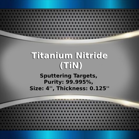
Applications of Sputtering Targets;
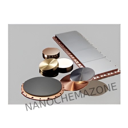
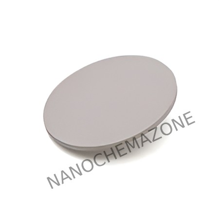
Film deposition is accomplished using sputtering targets. A technique for sputtering thin films is called "deposition made by sputter targets," which entails eroding material from a "target" source onto a "substrate" like a silicon wafer.
Etching of the target is done using semiconductor sputtering targets. When selectivity is not an issue and a high degree of etching anisotropy is required, sputter etching is the method of choice.
By removing the target material through etching, sputter targets are also utilized for investigation.
In secondary ion spectroscopy (SIMS), one example is when the target material is sputtered at a steady pace. When the target shatters,
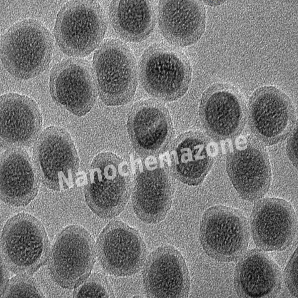
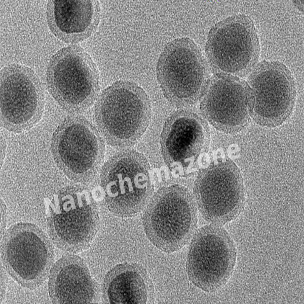
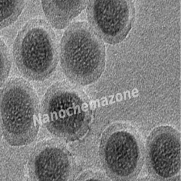
Mass spectrometry measures the concentration and identity of sputtered atoms. The target material's composition may be ascertained and even very low concentrations of contaminants can be found with the aid of the sputtering target.
There is also an application area for sputtering targets in space. One type of space weathering that alters the chemical and physical characteristics of airless worlds like the Moon and asteroids is sputtering.
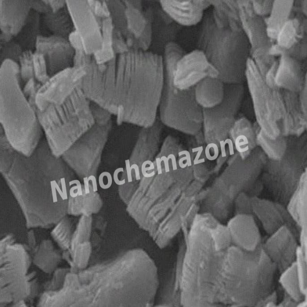
A solid mixture of barium titanate (BaTiO3) and strontium titanate (SrTiO3) is called barium strontium titanate (BST). Sputtering techniques yield thin coatings of barium strontium titanate (BST), which confers exceptional dielectric characteristics to materials. Due to this, BST-based barium strontium titanate
The past ten years have seen a rise in the popularity of ferroelectric thin film devices because of its numerous uses in tunable microwave devices, including phase shifters, delay lines, resonators, and varactors.
Thin films of barium strontium titanate show great promise because of their low dielectric loss, high dielectric constant, and tunability. There have been reports on the dielectric-tunable properties of barium strontium titanate films produced by various deposition processes. These properties investigate the impacts of several parameters, including grain size, Ba/Sr ratio, oxygen vacancies, and film thickness. To get more tunability and less loss, researchers have also looked at doping concentrations, high temperature annealing, and multilayer architectures.