Barium Fluoride (BaF2) Sputtering Targets, Purity: 99.99%, Size: 3”, Thickness: 0.125”

$1,348.00

Product 

Barium Fluoride (BaF2) Sputtering Targets, Purity: 99.99%, Size: 3'', Thickness: 0.125''

CAS No.

 7787-32-8

Appearance

Powder

Purity

≥99%,  ≥99.9%,  ≥95%

(Other purities are also available)

APS

< 5 µm (Size Can be customized), Ask for other available size ranges.

Ingredient

N/A

Molecular Weight

175.32 g/mol

Melting Point

 1,368 °C

Boiling Point

2,260 °C

Density

 4.89 g/cm³

Product Codes

NCZ-2485K

Lanthanum Nickel Oxide (LaNiO3) Sputtering Targets, Purity: 99.9%, Size: 4”, Thickness: 0.125”

$1,350.00

Applications of Sputtering Targets;

  • Sputtering targets is used for film deposition. The deposition made by sputter targets is a method of depositing thin films by sputtering that involves eroding material from a "target" source onto a "substrate" such as  a silicon wafer.
  • Semiconductor sputtering targets is used to etch the target. Sputter etching is chosen in cases where a high degree of etching anisotropy is needed and selectivity is not a concern.
  • Sputter targets is also used for analysis by etching away the target material.
One of the example occurs in secondary ion spectroscopy (SIMS), where the target sample is sputtered at a constant rate. As the target is sputtered, the concentration and identity of sputtered atoms are measured using mass spectrometry. By helping of the sputtering target, the composition of the target material can be determined and even extremely low concentrations of impurities are detected. Sputtering target has also application area in space. Sputtering is one of the forms of space weathering, a process that changes the physical and chemical properties of airless bodies, such as asteroids and the Moon. Lanthanum nickel oxide with the chemical formula of LaNiO3 is an important perovskite-type oxide with metallic conductivity. Lanthanum nickel oxide is a ternary compound with unique chemical and physical properties. It shows an extended range of oxygen-deficient compositions, an uncommon intrinsic n-type metallic conductance, a perovskite crystal structure and thermal and chemical stability. These characteristics make LNO a technologically important perovskite oxide electrode in many potential applications such as ferroelectric thin film capacitors, solid oxide fuel cells, nonvolatile ferroelectric random access memories and multilayer actuators. Furthermore, LNO films have potential to be used as oxygen pressure and ethanol active sensing layers. Also, the reduced La–Ni mixed oxides are reported to be good catalyst precursors to synthesized organic compounds and to grow large amounts of regular diameter distribution controlled carbon nanotubes. Different chemical and physical thin film deposition techniques have been used to prepare LNO on various substrates. Chemical methods such as chemical vapor deposition, metallo-organic chemical vapor deposition and chemical solution deposition have been used to prepare LNO films. Physical methods such as sputtering, pulsed laser deposition and mist plasma evaporation have also been reported. Wet chemical solution deposition techniques provide simple and versatile alternative methods for thin film preparation.

Bismuth Ferrite (BiFeO3) Sputtering Targets, Purity: 99.9%, Size: 8”, Thickness: 0.250”

$1,350.00

Applications of Sputtering Targets;

Film deposition is accomplished using sputtering targets. One technique for sputtering thin films is the deposition produced by sputter targets. It entails transferring material onto a "substrate," like a silicon wafer, from a "target" source. Etching of the target is done using semiconductor sputtering targets. When etching anisotropy is high, sputter etching is the preferred method. is required, and selectivity is unimportant. By removing the target material through etching, sputter targets are also utilized for investigation. In secondary ion spectroscopy (SIMS), one example is when the target material is sputtered at a steady pace. When the target shatters, Mass spectrometry measures the concentration and identity of sputtered atoms.

Cerium Oxide (CeO2) Sputtering Targets, Purity: 99.99%, Size: 6”, Thickness: 0.250”

$1,350.00

Applications of Sputtering Targets;

Film deposition is accomplished using sputtering targets. A technique for sputtering thin films is called "deposition made by sputter targets," which entails eroding material from a "target" source onto a "substrate" like a silicon wafer. Etching of the target is done using semiconductor sputtering targets. When selectivity is not an issue and a high degree of etching anisotropy is required, sputter etching is the method of choice. By removing the target material through etching, sputter targets are also utilized for investigation. In secondary ion spectroscopy (SIMS), one example is when the target material is sputtered at a steady pace. Mass spectrometry is used to quantify the concentration and identity of spewed atoms as the target is sputtered.

The target material's composition may be ascertained and even very low concentrations of contaminants can be found with the aid of the sputtering target.

There is also an application area for sputtering targets in space. One type of space weathering that alters the chemical and physical characteristics of airless worlds like the Moon and asteroids is sputtering.

The most prevalent rare-earth element in the crust of the earth is cerium, a metal that belongs to the lanthanide series. Cerium oxide's high refractive index and dielectric constant make it suitable for a wide range of optical and electrical applications. Additionally, cerium oxide can be used for corrosion protection coatings rather than coatings based on chromate.

Indium Tin Oxide/ITO (In203:Sn02) Sputtering Targets, Purity: 99.99%, Size: 8”, Thickness: 0.250”

$1,350.00

Applications of Sputtering Targets;

Film deposition is accomplished using sputtering targets. A technique for sputtering thin films is called "deposition made by sputter targets," which entails eroding material from a "target" source onto a "substrate" like a silicon wafer. Etching of the target is done using semiconductor sputtering targets. When selectivity is not an issue and a high degree of etching anisotropy is required, sputter etching is the method of choice. By removing the target material through etching, sputter targets are also utilized for investigation. In secondary ion spectroscopy (SIMS), one example is when the target material is sputtered at a steady pace. Mass spectrometry is used to quantify the concentration and identity of spewed atoms as the target is sputtered.

The target material's composition may be ascertained and even very low concentrations of contaminants can be found with the aid of the sputtering target.

There is also an application area for sputtering targets in space. One type of space weathering that alters the chemical and physical characteristics of airless worlds like the Moon and asteroids is sputtering.

Cerium Oxide (CeO2) Sputtering Targets, indium, Purity: 99.99%, Size: 3”, Thickness: 0.125”

$1,353.00

Applications of Sputtering Targets;

Film deposition is accomplished using sputtering targets. A technique for sputtering thin films is called "deposition made by sputter targets," which entails eroding material from a "target" source onto a "substrate" like a silicon wafer. Etching of the target is done using semiconductor sputtering targets. When selectivity is not an issue and a high degree of etching anisotropy is required, sputter etching is the method of choice. By removing the target material through etching, sputter targets are also utilized for investigation. In secondary ion spectroscopy (SIMS), one example is when the target material is sputtered at a steady pace. Mass spectrometry is used to quantify the concentration and identity of spewed atoms as the target is sputtered.

The target material's composition may be ascertained and even very low concentrations of contaminants can be found with the aid of the sputtering target.

There is also an application area for sputtering targets in space. One type of space weathering that alters the chemical and physical characteristics of airless worlds like the Moon and asteroids is sputtering.

The most prevalent rare-earth element in the crust of the earth is cerium, a metal that belongs to the lanthanide series. Cerium oxide's high refractive index and dielectric constant make it suitable for a wide range of optical and electrical applications. Additionally, cerium oxide can be used for corrosion protection coatings rather than coatings based on chromate.

Cerium Oxide (CeO2) Sputtering Targets, Purity: 99.99%, Size: 7”, Thickness: 0.125”

$1,355.00

Applications of Sputtering Targets;

Film deposition is accomplished using sputtering targets. A technique for sputtering thin films is called "deposition made by sputter targets," which entails eroding material from a "target" source onto a "substrate" like a silicon wafer. Etching of the target is done using semiconductor sputtering targets. When selectivity is not an issue and a high degree of etching anisotropy is required, sputter etching is the method of choice. By removing the target material through etching, sputter targets are also utilized for investigation. In secondary ion spectroscopy (SIMS), one example is when the target material is sputtered at a steady pace. Mass spectrometry is used to quantify the concentration and identity of spewed atoms as the target is sputtered.

The target material's composition may be ascertained and even very low concentrations of contaminants can be found with the aid of the sputtering target.

There is also an application area for sputtering targets in space. One type of space weathering that alters the chemical and physical characteristics of airless worlds like the Moon and asteroids is sputtering.

The most prevalent rare-earth element in the crust of the earth is cerium, a metal that belongs to the lanthanide series. Cerium oxide's high refractive index and dielectric constant make it suitable for a wide range of optical and electrical applications. Additionally, cerium oxide can be used for corrosion protection coatings rather than coatings based on chromate.

Nickel Oxide (NiO) Sputtering Targets, indium, Purity: 99.95%, Size: 3”, Thickness: 0.125”

$1,355.00

Product 

Nickel Oxide (NiO) Sputtering Targets, indium, Purity: 99.95%, Size: 3'', Thickness: 0.125''

CAS No.

1313-99-1

Appearance

Powder

Purity

≥99%,  ≥99.9%,  ≥95%

(Other purities are also available)

APS

 ~3–5 µm (Size Can be customized), Ask for other available size ranges.

Ingredient

N/A

Molecular Weight

74.69 g/mol

Melting Point

1,950 °C

Boiling Point

 2,730 °C

Density

 6.67 g/cm³

Product Codes

NCZ-1831K

Aluminum Oxide (Al2O3) Sputtering Targets, Purity: 99.99%, Size: 8”, Thickness: 0.250”

$1,355.00

Product 

Aluminum Oxide (Al2O3) Sputtering Targets, Purity: 99.99%, Size: 8'', Thickness: 0.250''

CAS No.

 1344-28-1

Appearance

Powder

Purity

≥99%,  ≥99.9%,  ≥95%

(Other purities are also available)

APS

N/A (Size Can be customized), Ask for other available size ranges.

Ingredient

N/A

Molecular Weight

101.96 g/mol

Melting Point

~2,072 °C

Boiling Point

~2,977 °C

Density

~3.97–3.98 g/cm³

Product Codes

NCZ-2528K

Aluminum Oxide (Al2O3) Sputtering Targets, Purity: 99.99%, Size: 8”, Thickness: 0.125”

$1,355.00

Product 

Aluminum Oxide (Al2O3) Sputtering Targets, Purity: 99.99%, Size: 8'', Thickness: 0.125''

CAS No.

 1344-28-1

Appearance

Powder

Purity

≥99%,  ≥99.9%,  ≥95%

(Other purities are also available)

APS

N/A (Size Can be customized), Ask for other available size ranges.

Ingredient

N/A

Molecular Weight

101.96 g/mol

Melting Point

~2,072 °C

Boiling Point

~2,977 °C

Density

~3.97–3.98 g/cm³

Product Codes

NCZ-2529K

Magnesium Oxide (MgO) Sputtering Targets, Purity: 99.95%, Size: 8”, Thickness: 0.250”

$1,356.00

Product 

Magnesium Oxide (MgO) Sputtering Targets, Purity: 99.95%, Size: 8'', Thickness: 0.250''

CAS No.

1309-48-4

Appearance

Powder

Purity

≥99%,  ≥99.9%,  ≥95%

(Other purities are also available)

APS

 N/A (Size Can be customized), Ask for other available size ranges.

Ingredient

N/A

Molecular Weight

40.30 g/mol

Melting Point

 ~2852 °C

Boiling Point

~3600 °C

Density

 ~3.58 g/cm³

Product Codes

NCZ-1961K

Bismuth Ferrite (BiFeO3) Sputtering Targets, indium, Purity: 99.9%, Size: 1”, Thickness: 0.125”

$1,357.00

Applications of Sputtering Targets;

Film deposition is accomplished using sputtering targets. A technique for sputtering thin films is called "deposition made by sputter targets," which entails eroding material from a "target" source onto a "substrate" like a silicon wafer. Etching of the target is done using semiconductor sputtering targets. When selectivity is not an issue and a high degree of etching anisotropy is required, sputter etching is the method of choice. By removing the target material through etching, sputter targets are also utilized for investigation. In secondary ion spectroscopy (SIMS), one example is when the target material is sputtered at a steady pace. Mass spectrometry is used to quantify the concentration and identity of spewed atoms as the target is sputtered.

The target material's composition may be ascertained and even very low concentrations of contaminants can be found with the aid of the sputtering target.

There is also an application area for sputtering targets in space. One type of space weathering that alters the chemical and physical characteristics of airless worlds like the Moon and asteroids is sputtering.

One of the most promising multiferroic materials is bismuth ferrite, an inorganic chemical compound with a perovskite structure and the chemical formula BiFeO3. In order to create a one-phase material called bismuth ferrite (BiFeO3), a bismuth ferrite sputtering target is often manufactured by high temperature sinttering or recrystallizing the mixture of the oxide compound of Bi and Fe. For targets that are sputtering bismuth ferrite, indium bonding is advised.

Bismuth Ferrite (BiFeO3) Sputtering Targets, indium, Purity: 99.9%, Size: 3”, Thickness: 0.125”

$1,357.00

Applications of Sputtering Targets;

Film deposition is accomplished using sputtering targets. A technique for sputtering thin films is called "deposition made by sputter targets," which entails eroding material from a "target" source onto a "substrate" like a silicon wafer. Etching of the target is done using semiconductor sputtering targets. When selectivity is not an issue and a high degree of etching anisotropy is required, sputter etching is the method of choice. By removing the target material through etching, sputter targets are also utilized for investigation. In secondary ion spectroscopy (SIMS), one example is when the target material is sputtered at a steady pace. Mass spectrometry is used to quantify the concentration and identity of spewed atoms as the target is sputtered.

The target material's composition may be ascertained and even very low concentrations of contaminants can be found with the aid of the sputtering target.

There is also an application area for sputtering targets in space. One type of space weathering that alters the chemical and physical characteristics of airless worlds like the Moon and asteroids is sputtering.

One of the most promising multiferroic materials is bismuth ferrite, an inorganic chemical compound with a perovskite structure and the chemical formula BiFeO3. In order to create a one-phase material called bismuth ferrite (BiFeO3), a bismuth ferrite sputtering target is often manufactured by high temperature sinttering or recrystallizing the mixture of the oxide compound of Bi and Fe. For targets that are sputtering bismuth ferrite, indium bonding is advised.

Lanthanum Manganate (LaMnO3) Sputtering Targets, Purity: 99.9%, Size: 3”, Thickness: 0.125”

$1,357.00

Product 

Lanthanum Manganate (LaMnO3) Sputtering Targets, Purity: 99.9%, Size: 3'', Thickness: 0.125''

CAS No.

13538-87-7

Appearance

Powder

Purity

≥99%,  ≥99.9%,  ≥95%

(Other purities are also available)

APS

 ~1–5 µm (Size Can be customized), Ask for other available size ranges.

Ingredient

N/A

Molecular Weight

240.83 g/mol

Melting Point

N/A

Boiling Point

N/A

Density

~6.3 – 6.8 g/cm³

Product Codes

NCZ-2139K

Tungsten Oxide (WO3) Sputtering Targets, Purity: 99.9%, Size: 3”, Thickness: 0.250”

$1,359.00

Product 

Tungsten Oxide (WO3) Sputtering Targets, Purity: 99.9%, Size: 3'', Thickness: 0.250''

CAS No.

1314-35-8

Appearance

Powder

Purity

≥99%,  ≥99.9%,  ≥95%

(Other purities are also available)

APS

N/A  (Size Can be customized), Ask for other available size ranges.

Ingredient

N/A

Molecular Weight

231.84 g/mol

Melting Point

1,473 °C

Boiling Point

1,700–1,850 °C

Density

7.16 g/cm³

Product Codes

NCZ-1569K

Cerium (Ce) Micron Powder, Purity: 99.5 %, Size: 325 mesh

Price range: $1,360.00 through $4,656.00
Select options This product has multiple variants. The options may be chosen on the product page

Applications:

Cerium is the most abundant element of the rare earth elements. It is found in minerals sallanite, rhabdophane, hydroxylbastnasite, bastnasite, monazite, synchysite, and zircon. It is ductile and it oxidizes very quickly at room temperature. Cerium nanoparticles are graded as highly flammable and harmful. Cerium powder is applied as polishing agent in glass polishing. It is very efficient glass polishing agents. It is used for precision optical polishing because of its strong oxidizing properties. It is also used to remove ultrafine diesel particle emissions like carbon. It is used in steel manufacturing to remove unwanted trace elements such as lead and antimony and to remove free oxygen and sulfur. Cerium powder has also applications in fuel cells functions for example it is used in the electrolyte of solid oxide fuel cells. 

Praseodymium Calcium Manganate (Pr0.7Ca0.3MnO3) Sputtering Targets, indium, Purity: 99.9%, Size: 2”, Thickness: 0.125”

$1,363.00

Product 

Praseodymium Calcium Manganate (Pr0.7Ca0.3MnO3) Sputtering Targets, indium, Purity: 99.9%, Size: 2'', Thickness: 0.125''

CAS No.

N/A

Appearance

Powder

Purity

≥99%,  ≥99.9%,  ≥95%

(Other purities are also available)

APS

1–5 μm (Size Can be customized), Ask for other available size ranges.

Ingredient

N/A

Molecular Weight

237.66 g/mol

Melting Point

N/A

Boiling Point

N/A

Density

~6.4–6.8 g/cm³

Product Codes

NCZ-1775K

>99% Violet Phosphorus Crystal, 200mg

$1,364.00
Product >99% Violet Phosphorus Crystal, 200mg
CAS No. 7723-14-0
Appearance Crystal with metallic luster
Purity ≥99%,  ≥99.9%,  ≥95%(Other purities are also available)
APS 50–500µm (Size Can be customized),  Ask for other available size range.
Ingredient P
Molecular Weight 30.97 g/mol
Melting Point 610 °C
Boiling Point N/A
Density 2.36 g/cm³
Product Codes NCZ-274I

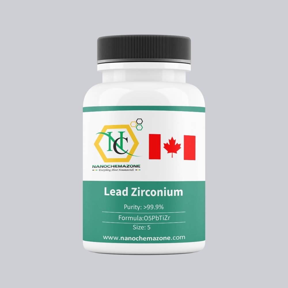
Lead Zirconium Titanate/PZT (O5PbTiZr) Sputtering Targets, Purity: 99.9%, Size: 3”, Thickness: 0.250”

$1,364.00

Product 

Lead Zirconium Titanate/PZT (O5PbTiZr) Sputtering Targets, Purity: 99.9%, Size: 3'', Thickness: 0.250''

CAS No.

12626-81-2

Appearance

Powder

Purity

≥99%,  ≥99.9%,  ≥95%

(Other purities are also available)

APS

 N/A (Size Can be customized), Ask for other available size ranges.

Ingredient

N/A

Molecular Weight

~303.1 g/mol

Melting Point

 ~1,250°C – 1,350°C

Boiling Point

N/A

Density

 ~7.75–8.0 g/cm³

Product Codes

NCZ-2065K

Bismuth Ferrite (BiFeO3) Sputtering Targets, Purity: 99.9%, Size: 5”, Thickness: 0.250”

$1,364.00

Product 

Bismuth Ferrite (BiFeO3) Sputtering Targets, Purity: 99.9%, Size: 5'', Thickness: 0.250''

CAS No.

 12010‑42‑3

Appearance

Powder

Purity

≥99%,  ≥99.9%,  ≥95%

(Other purities are also available)

APS

 0.5–2 µm (Size Can be customized), Ask for other available size ranges.

Ingredient

N/A

Molecular Weight

~312.82 g/mol

Melting Point

 ~1255 °C (bulk material)

Boiling Point

N/A

Density

~8.22 g/cm³

Product Codes

NCZ-2422K

Cerium Oxide (CeO2) Sputtering Targets, Purity: 99.99%, Size: 5”, Thickness: 0.250”

$1,365.00

Product 

Cerium Oxide (CeO2) Sputtering Targets, Purity: 99.99%, Size: 5'', Thickness: 0.250''

CAS No.

 1306-38-3

Appearance

Powder

Purity

≥99%,  ≥99.9%,  ≥95%

(Other purities are also available)

APS

 N/A (Size Can be customized), Ask for other available size ranges.

Ingredient

N/A

Molecular Weight

 172.11 g/mol

Melting Point

2,400–2,600 °C

Boiling Point

Sublimes above 3,000 °C

Density

 7.13 g/cm³

Product Codes

NCZ-2325K

Barium Strontium Titanate (BaO4SrTi) Sputtering Targets, elastomer, Purity: 99.99%, Size: 4”, Thickness: 0.125”

$1,366.00

Applications of Sputtering Targets;

Film deposition is accomplished using sputtering targets. A technique for sputtering thin films is called "deposition made by sputter targets," which entails eroding material from a "target" source onto a "substrate" like a silicon wafer. Etching of the target is done using semiconductor sputtering targets. When selectivity is not an issue and a high degree of etching anisotropy is required, sputter etching is the method of choice. By removing the target material through etching, sputter targets are also utilized for investigation. In secondary ion spectroscopy (SIMS), one example is when the target material is sputtered at a steady pace. When the target shatters,

Mass spectrometry measures the concentration and identity of sputtered atoms. The target material's composition may be ascertained and even very low concentrations of contaminants can be found with the aid of the sputtering target.

There is also an application area for sputtering targets in space. One type of space weathering that alters the chemical and physical characteristics of airless worlds like the Moon and asteroids is sputtering.

A solid mixture of barium titanate (BaTiO3) and strontium titanate (SrTiO3) is called barium strontium titanate (BST). Sputtering techniques yield thin coatings of barium strontium titanate (BST), which confers exceptional dielectric characteristics to materials. As a result, over the past ten years, barium strontium titanate (BST) based ferroelectric thin film devices have gained popularity because of its

phase shifters, varactors, and resonators.

Thin films of barium strontium titanate show great promise because of their low dielectric loss, high dielectric constant, and tunability. There have been reports on the dielectric-tunable properties of barium strontium titanate films produced by various deposition processes. These properties investigate the impacts of several parameters, including grain size, Ba/Sr ratio, oxygen vacancies, and film thickness. To get more tunability and less loss, researchers have also looked at doping concentrations, high temperature annealing, and multilayer architectures.

Aluminum Nitride (AlN) Sputtering Targets, Purity: 99.8%, Size: 4”, Thickness: 0.125”

$1,366.00

Product 

Aluminum Nitride (AlN) Sputtering Targets, Purity: 99.8%, Size: 4'', Thickness: 0.125''

CAS No.

 24304-00-5

Appearance

Powder

Purity

≥99%,  ≥99.9%,  ≥95%

(Other purities are also available)

APS

N/A (Size Can be customized), Ask for other available size ranges.
Ingredient

N/A

Molecular Weight

40.99 g/mol

Melting Point

 ~2200 °C

Boiling Point

 N/A

Density

 ~3.26 g/cm³

Product Codes

NCZ-2555K

Titanium Dioxide (TiO2) Sputtering Targets, Purity: 99.99%, Size: 3”, Thickness: 0.250”, Beige to White

$1,369.00

Product 

Titanium Dioxide (TiO2) Sputtering Targets, Purity: 99.99%, Size: 3'', Thickness: 0.250'', Beige to White

CAS No.

13463‑67‑7

Appearance

Powder

Purity

≥99%,  ≥99.9%,  ≥95%

(Other purities are also available)

APS

TiO₂ (black granules) (Size Can be customized), Ask for other available size ranges.
Ingredient

N/A

Molecular Weight

79.94 g/mol

Melting Point

~1,843 °C

Boiling Point

~2,972 °C

Density

~4.23 g/cm³

Product Codes

NCZ-1434K

Impending Self-Help Transfer Nickel Graphene Foam, Thickness: 1±0.1 mm, Size: 5×10 cm

Price range: $1,373.00 through $5,472.00
Select options This product has multiple variants. The options may be chosen on the product page
1 piece/ 1373 € 5 pieces/ 5472 €  Contact us for tailored quotes on larger quantities & experience exceptional solutions from our experts.

Cerium Oxide (CeO2) Sputtering Targets, Purity: 99.99%, Size: 4”, Thickness: 0.250”

$1,374.00

Product 

Cerium Oxide (CeO2) Sputtering Targets, Purity: 99.99%, Size: 4'', Thickness: 0.250''

CAS No.

 1306-38-3

Appearance

Powder

Purity

≥99%,  ≥99.9%,  ≥95%

(Other purities are also available)

APS

 N/A (Size Can be customized), Ask for other available size ranges.

Ingredient

N/A

Molecular Weight

 172.11 g/mol

Melting Point

2,400–2,600 °C

Boiling Point

Sublimes above 3,000 °C

Density

 7.13 g/cm³

Product Codes

NCZ-2327K

Lanthanum Nickel Oxide (LaNiO3) Sputtering Targets, indium, Purity: 99.9%, Size: 2”, Thickness: 0.125”

$1,377.00

Product 

Lanthanum Nickel Oxide (LaNiO3) Sputtering Targets, indium, Purity: 99.9%, Size: 2'', Thickness: 0.125''

CAS No.

12031‑18‑4

Appearance

Powder

Purity

≥99%,  ≥99.9%,  ≥95%

(Other purities are also available)

APS

 ~1–5 µm (Size Can be customized), Ask for other available size ranges.

Ingredient

N/A

Molecular Weight

~245.6 g/mol

Melting Point

N/A

Boiling Point

N/A

Density

~6.25–7.0 g/cm³

Product Codes

NCZ-2110K

Lanthanum Nickel Oxide (LaNiO3) Sputtering Targets, Purity: 99.9%, Size: 3”, Thickness: 0.125”

$1,377.00

Product 

Lanthanum Nickel Oxide (LaNiO3) Sputtering Targets, Purity: 99.9%, Size: 3'', Thickness: 0.125''

CAS No.

12031‑18‑4

Appearance

Powder

Purity

≥99%,  ≥99.9%,  ≥95%

(Other purities are also available)

APS

 ~1–5 µm (Size Can be customized), Ask for other available size ranges.

Ingredient

N/A

Molecular Weight

 ~245.6 g/mol

Melting Point

Decomposes at ~1300–1500 °C

Boiling Point

N/A

Density

 ~6.5–7.0 g/cm³

Product Codes

NCZ-2123K

Antimony Telluride (Sb2Te3) Sputtering Targets, Purity: 99.999%, Size: 4”, Thickness: 0.250”

$1,380.00

Applications of Sputtering Targets;

Film deposition is accomplished using sputtering targets. A technique for sputtering thin films is called "deposition made by sputter targets," which entails eroding material from a "target" source onto a "substrate" like a silicon wafer. Etching of the target is done using semiconductor sputtering targets. When selectivity is not an issue and a high degree of etching anisotropy is required, sputter etching is the method of choice. By removing the target material through etching, sputter targets are also utilized for investigation. In secondary ion spectroscopy (SIMS), one example is when the target material is sputtered at a steady pace. Mass spectrometry is used to quantify the concentration and identity of spewed atoms as the target is sputtered. With the sputtering target's assistance, the

It is possible to identify the target material and even detect incredibly tiny impurity amounts.

There is also an application area for sputtering targets in space. One type of space weathering that alters the chemical and physical characteristics of airless worlds like the Moon and asteroids is sputtering.

The chemical formula for antimony telluride, an inorganic molecule, is Sb2Te3. It has a layered structure and is a grey crystalline solid. Layers are kept together by weak van der Waals forces and are composed of two antimony atomic sheets and three tellurium atomic sheets.

Let's now examine the regions in which antimony telluride sputtering targets are used. As far as we are aware, thermoelectric devices have garnered significant interest due toBecause they can directly convert heat into electric energy, they can be used as power generators, coolers, and thermal sensors or detectors. The power factor or the dimensionless figure of merit (ZT) of the materials are used to assess thermoelectric device performance. Tellurium antimony (Sb2Te3)

Antimony Telluride (Sb2Te3) Sputtering Targets, Purity: 99.999%, Size: 4”, Thickness: 0.125”

$1,380.00

Applications of Sputtering Targets;

Film deposition is accomplished using sputtering targets. One technique for sputtering thin films is the deposition produced by sputter targets. It entails transferring material onto a "substrate," like a silicon wafer, from a "target" source. Etching of the target is done using semiconductor sputtering targets. When etching anisotropy is high, sputter etching is the preferred method. is required, and selectivity is unimportant. By removing the target material through etching, sputter targets are also utilized for investigation. In secondary ion spectroscopy (SIMS), one example is when the target material is sputtered at a steady pace. When the target shatters, Mass spectrometry measures the concentration and identity of sputtered atoms. With the sputtering target's assistance, the It is possible to identify the target material and even detect incredibly tiny impurity amounts. There is also an application area for sputtering targets in space. One type of space weathering that alters the chemical and physical characteristics of airless worlds like the Moon and asteroids is sputtering. The chemical formula for antimony telluride, an inorganic molecule, is Sb2Te3. It has a layered structure and is a grey crystalline solid. Weak van der Waals forces hold the layers together. They are made up of three atomic sheets of tellurium and two atomic sheets of antimony.

Barium Fluoride (BaF2) Sputtering Targets, Purity: 99.99%, Size: 4”, Thickness: 0.250”

$1,380.00

Applications of Sputtering Targets;

Film deposition is accomplished using sputtering targets. A technique for sputtering thin films is called "deposition made by sputter targets," which entails eroding material from a "target" source onto a "substrate" like a silicon wafer. Etching of the target is done using semiconductor sputtering targets. When selectivity is not an issue and a high degree of etching anisotropy is required, sputter etching is the method of choice. By removing the target material through etching, sputter targets are also utilized for investigation. In secondary ion spectroscopy (SIMS), one example is when the target material is sputtered at a steady pace. When the target shatters,

Mass spectrometry measures the concentration and identity of sputtered atoms. The target material's composition may be ascertained and even very low concentrations of contaminants can be found with the aid of the sputtering target.

There is also an application area for sputtering targets in space. One type of space weathering that alters the chemical and physical characteristics of airless worlds like the Moon and asteroids is sputtering.

A chemical compound consisting of barium and fluorine, barium fluoride (BaF2) is a salt. It is a solid that has the potential to be a clear crystal. A is barium fluoride.

Barium Fluoride (BaF2) Sputtering Targets, Purity: 99.99%, Size: 4”, Thickness: 0.125”

$1,380.00

Applications of Sputtering Targets;

Film deposition is accomplished using sputtering targets. A technique for sputtering thin films is called "deposition made by sputter targets," which entails eroding material from a "target" source onto a "substrate" like a silicon wafer. Etching of the target is done using semiconductor sputtering targets. When selectivity is not an issue and a high degree of etching anisotropy is required, sputter etching is the method of choice. By removing the target material through etching, sputter targets are also utilized for investigation. In secondary ion spectroscopy (SIMS), one example is when the target material is sputtered at a steady pace. Mass spectrometry is used to quantify the concentration and identity of spewed atoms as the target is sputtered. With the sputtering target's assistance, the

It is possible to identify the target material and even detect incredibly tiny impurity amounts.

There is also an application area for sputtering targets in space. One type of space weathering that alters the chemical and physical characteristics of airless worlds like the Moon and asteroids is sputtering.

A chemical compound consisting of barium and fluorine, barium fluoride (BaF2) is a salt. It is a solid that has the potential to be a clear crystal. One chemical compound for the 10–20 µm wavelength infrared area is barium fluoride. Enamel, glazing frits, and aluminum metallurgy all use barium fluoride.

Cerium Oxide (CeO2) Sputtering Targets, Purity: 99.99%, Size: 7”, Thickness: 0.250”

$1,380.00

Applications of Sputtering Targets;

Film deposition is accomplished using sputtering targets. A technique for sputtering thin films is called "deposition made by sputter targets," which entails eroding material from a "target" source onto a "substrate" like a silicon wafer. Etching of the target is done using semiconductor sputtering targets. When selectivity is not an issue and a high degree of etching anisotropy is required, sputter etching is the method of choice. By removing the target material through etching, sputter targets are also utilized for investigation. In secondary ion spectroscopy (SIMS), one example is when the target material is sputtered at a steady pace. Mass spectrometry is used to quantify the concentration and identity of spewed atoms as the target is sputtered.

The target material's composition may be ascertained and even very low concentrations of contaminants can be found with the aid of the sputtering target.

There is also an application area for sputtering targets in space. One type of space weathering that alters the chemical and physical characteristics of airless worlds like the Moon and asteroids is sputtering.

The most prevalent rare-earth element in the crust of the earth is cerium, a metal that belongs to the lanthanide series. Cerium oxide's high refractive index and dielectric constant make it suitable for a wide range of optical and electrical applications. Additionally, cerium oxide can be used for corrosion protection coatings rather than coatings based on chromate.

Lead Zirconium Titanate/PZT (O5PbTiZr) Sputtering Targets, Purity: 99.9%, Size: 5”, Thickness: 0.125”

$1,381.00

Product 

Lead Zirconium Titanate/PZT (O5PbTiZr) Sputtering Targets, Purity: 99.9%, Size: 5'', Thickness: 0.125''

CAS No.

12626-81-2

Appearance

Powder

Purity

≥99%,  ≥99.9%,  ≥95%

(Other purities are also available)

APS

 N/A (Size Can be customized), Ask for other available size ranges.

Ingredient

N/A

Molecular Weight

~303.1 g/mol

Melting Point

 ~1,250°C – 1,350°C

Boiling Point

N/A

Density

 ~7.75–8.0 g/cm³

Product Codes

NCZ-2062K

Lead Zirconium Titanate/PZT (O5PbTiZr) Sputtering Targets, Purity: 99.9%, Size: 5”, Thickness: 0.250”

$1,382.00

Applications of Sputtering Targets;

Film deposition is accomplished using sputtering targets. A technique for sputtering thin films is called "deposition made by sputter targets," which entails eroding material from a "target" source onto a "substrate" like a silicon wafer. Etching of the target is done using semiconductor sputtering targets. When selectivity is not an issue and a high degree of etching anisotropy is required, sputter etching is the method of choice. By removing the target material through etching, sputter targets are also utilized for investigation. In secondary ion spectroscopy (SIMS), one example is when the target material is sputtered at a steady pace. Mass spectrometry is used to quantify the concentration and identity of spewed atoms as the target is sputtered.

The target material's composition may be ascertained and even very low concentrations of contaminants can be found with the aid of the sputtering target.

There is also an application area for sputtering targets in space. One type of space weathering that alters the chemical and physical characteristics of airless worlds like the Moon and asteroids is sputtering.

An inorganic substance is lead zirconium titanate. This ceramic perovskite material has a strong piezoelectric effect, which means that when an electric field is applied, the compound changes shape. Lead zirconium titanate is employed in a number of practical applications such as ultrasonic transducers and piezoelectric resonators.

Lanthanum Manganate (LaMnO3) Sputtering Targets, Purity: 99.9%, Size: 4”, Thickness: 0.125”

$1,384.00

Product 

Lanthanum Manganate (LaMnO3) Sputtering Targets, Purity: 99.9%, Size: 4'', Thickness: 0.125''

CAS No.

13538-87-7

Appearance

Powder

Purity

≥99%,  ≥99.9%,  ≥95%

(Other purities are also available)

APS

 ~1–5 µm (Size Can be customized), Ask for other available size ranges.

Ingredient

N/A

Molecular Weight

240.83 g/mol

Melting Point

 ~2300 °C

Boiling Point

N/A

Density

~6.3 – 6.8 g/cm³

Product Codes

NCZ-2137K

Graphene Oxides (98%, <2nm, diameter: 8~15um)

$1,385.00
Select options This product has multiple variants. The options may be chosen on the product page
$293/1g $1385/5g
Product Graphene Oxides (98%, <2nm, diameter: 8~15um)
CAS No. 1034343-98-0
Appearance Black powder
Purity ≥99%,  ≥99.9%,  ≥95%(Other purities are also available)
APS 8-15nm (Size Can be customized),  Ask for other available size range.
Ingredient (C)x(OH)yOz
Molecular Weight N/A
Melting Point N/A
Boiling Point N/A
Density 2.2 g/cm³
Product Codes NCZ-112G
 

Magnesium Oxide (MgO) Sputtering Targets, Purity: 99.95%, Size: 4”, Thickness: 0.125”

$1,387.00

Applications of Sputtering Targets;

Film deposition is accomplished using sputtering targets. A technique for sputtering thin films is called "deposition made by sputter targets," which entails eroding material from a "target" source onto a "substrate" like a silicon wafer. Etching of the target is done using semiconductor sputtering targets. When selectivity is not an issue and a high degree of etching anisotropy is required, sputter etching is the method of choice. By removing the target material through etching, sputter targets are also utilized for investigation. In secondary ion spectroscopy (SIMS), one example is when the target material is sputtered at a steady pace. Mass spectrometry is used to quantify the concentration and identity of spewed atoms as the target is sputtered.

By helping of the sputtering target, the composition of the target material may be evaluated and even extremely tiny amounts of contaminants are recognized.

There is also an application area for sputtering targets in space. One type of space weathering that alters the chemical and physical characteristics of airless worlds like the Moon and asteroids is sputtering.

Bismuth Ferrite (BiFeO3) Sputtering Targets, Purity: 99.9%, Size: 7”, Thickness: 0.125”

$1,387.00

Product 

Bismuth Ferrite (BiFeO3) Sputtering Targets, Purity: 99.9%, Size: 7'', Thickness: 0.125''

CAS No.

 12010‑42‑3

Appearance

Powder

Purity

≥99%,  ≥99.9%,  ≥95%

(Other purities are also available)

APS

 0.5–2 µm (Size Can be customized), Ask for other available size ranges.

Ingredient

N/A

Molecular Weight

~312.82 g/mol

Melting Point

 ~1255 °C (bulk material)

Boiling Point

N/A

Density

~8.22 g/cm³

Product Codes

NCZ-2419K

Titanium Nitride (TiN) Sputtering Targets, indium, Purity: 99.5%, Size: 4”, Thickness: 0.125”

$1,389.00

Applications of Sputtering Targets;

Film deposition is accomplished using sputtering targets. A technique for sputtering thin films is called "deposition made by sputter targets," which entails eroding material from a "target" source onto a "substrate" like a silicon wafer. Etching of the target is done using semiconductor sputtering targets. When selectivity is not an issue and a high degree of etching anisotropy is required, sputter etching is the method of choice. By removing the target material through etching, sputter targets are also utilized for investigation. In secondary ion spectroscopy (SIMS), one example is when the target material is sputtered at a steady pace. Mass spectrometry is used to quantify the concentration and identity of spewed atoms as the target is sputtered.

The target material's composition may be ascertained and even very low concentrations of contaminants can be found with the aid of the sputtering target.

There is also an application area for sputtering targets in space. One type of space weathering that alters the chemical and physical characteristics of airless worlds like the Moon and asteroids is sputtering.

Cerium Oxide (CeO2) Sputtering Targets, Purity: 99.99%, Size: 8”, Thickness: 0.250”

$1,390.00

Applications of Sputtering Targets;

Film deposition is accomplished using sputtering targets. A technique for sputtering thin films is called "deposition made by sputter targets," which entails eroding material from a "target" source onto a "substrate" like a silicon wafer. Etching of the target is done using semiconductor sputtering targets. When selectivity is not an issue and a high degree of etching anisotropy is required, sputter etching is the method of choice. By removing the target material through etching, sputter targets are also utilized for investigation. In secondary ion spectroscopy (SIMS), one example is when the target material is sputtered at a steady pace. Mass spectrometry is used to quantify the concentration and identity of spewed atoms as the target is sputtered.

The target material's composition may be ascertained and even very low concentrations of contaminants can be found with the aid of the sputtering target.

There is also an application area for sputtering targets in space. One type of space weathering that alters the chemical and physical characteristics of airless worlds like the Moon and asteroids is sputtering.

The most prevalent rare-earth element in the crust of the earth is cerium, a metal that belongs to the lanthanide series. Cerium oxide's high refractive index and dielectric constant make it suitable for a wide range of optical and electrical applications. Additionally, cerium oxide can be used for corrosion protection coatings rather than coatings based on chromate.

Chromium Oxide (Cr2O3) Sputtering Targets, Purity: 99.8%, Size: 4”, Thickness: 0.125”

$1,390.00

Product 

Chromium Oxide (Cr2O3) Sputtering Targets, Purity: 99.8%, Size: 4'', Thickness: 0.125''

CAS No.

1308‑38‑9

Appearance

Powder

Purity

≥99%,  ≥99.9%,  ≥95%

(Other purities are also available)

APS

 N/A (Size Can be customized), Ask for other available size ranges.

Ingredient

N/A

Molecular Weight

 151.99 g/mol

Melting Point

~2,435 °C

Boiling Point

~3,000 °C (approximate; oxide may decompose before boiling)

Density

 ~5.21–5.22 g/cm³

Product Codes

NCZ-2296K

Bismuth Ferrite (BiFeO3) Sputtering Targets, Purity: 99.9%, Size: 6”, Thickness: 0.250”

$1,399.00

Product 

Bismuth Ferrite (BiFeO3) Sputtering Targets, Purity: 99.9%, Size: 6'', Thickness: 0.250''

CAS No.

 12010‑42‑3

Appearance

Powder

Purity

≥99%,  ≥99.9%,  ≥95%

(Other purities are also available)

APS

 0.5–2 µm (Size Can be customized), Ask for other available size ranges.

Ingredient

N/A

Molecular Weight

~312.82 g/mol

Melting Point

 ~1255 °C (bulk material)

Boiling Point

N/A

Density

~8.22 g/cm³

Product Codes

NCZ-2420K

Barium Zirconate (BaZrO3) Sputtering Targets, Purity: 99.99%, Size: 4”, Thickness: 0.125”

$1,399.00

Product 

Barium Zirconate (BaZrO3) Sputtering Targets, Purity: 99.99%, Size: 4'', Thickness: 0.125''

CAS No.

12009‑21‑1

Appearance

Powder

Purity

≥99%,  ≥99.9%,  ≥95%

(Other purities are also available)

APS

1 – 5 µm (Size Can be customized), Ask for other available size ranges.

Ingredient

N/A

Molecular Weight

276.55 g/mol

Melting Point

N/A

Boiling Point

N/A

Density

~5.52 g/cm³ (theoretical)

Product Codes

NCZ-2442K

Calcium Manganate (CaMnO3) Sputtering Targets, indium, Purity: 99.9%, Size: 3”, Thickness: 0.125”

$1,406.00

Product 

Calcium Manganate (CaMnO3) Sputtering Targets, indium, Purity: 99.9%, Size: 3'', Thickness: 0.125''

CAS No.

12058-85-6

Appearance

Powder

Purity

≥99%,  ≥99.9%,  ≥95%

(Other purities are also available)

APS

 N/A (Size Can be customized), Ask for other available size ranges.

Ingredient

N/A

Molecular Weight

157.87 g/mol

Melting Point

 Approx. 1400 °C (decomposes)

Boiling Point

N/A

Density

 ~4.7 g/cm³

Product Codes

NCZ-2355K

Lanthanum Strontium Manganate (La0.7Sr0.3MnO3) Sputtering Targets, Purity: 99.9%, Size: 4”, Thickness: 0.250”

$1,411.00

Product 

Lanthanum Strontium Manganate (La0.7Sr0.3MnO3) Sputtering Targets, Purity: 99.9%, Size: 4'', Thickness: 0.250''

CAS No.

 68189‑52‑4

Appearance

Powder

Purity

≥99%,  ≥99.9%,  ≥95%

(Other purities are also available)

APS

<5 µm (Size Can be customized), Ask for other available size ranges.

Ingredient

N/A

Molecular Weight

~234–237 g/mol

Melting Point

N/A

Boiling Point

N/A

Density

~6.3–6.5 g/cm³

Product Codes

NCZ-2102K

Impending Self-Help Transfer Nickel Graphene Foam, Thickness: 1±0.1 mm, Size: 5×10 cm

Price range: $1,415.00 through $5,302.00
Select options This product has multiple variants. The options may be chosen on the product page
Please contact us for quotes for larger quantities !   Impending self-help transfer nickel graphene foam is produced by etching the nickel of nickel graphene foam in etching liquid and being transferred to impending substrate. Graphene foam, can be gently released in deionized water and transferred directly to any base. This product is widely used for producing sensors, super capacitors and as the electrode materials of lithium battery to improve the battery capacity.

Aluminum Nitride (AlN) Sputtering Targets, Purity: 99.8%, Size:4”, Thickness: 0.250”

$1,415.00

Product 

Aluminum Nitride (AlN) Sputtering Targets, Purity: 99.8%, Size:4'', Thickness: 0.250''

CAS No.

 24304-00-5

Appearance

Powder

Purity

≥99%,  ≥99.9%,  ≥95%

(Other purities are also available)

APS

N/A (Size Can be customized), Ask for other available size ranges.

Ingredient

N/A

Molecular Weight

40.99 g/mol

Melting Point

 ~2200 °C

Boiling Point

 N/A

Density

 ~3.26 g/cm³

Product Codes

NCZ-2554K

Lanthanum Manganate (LaMnO3) Sputtering Targets, Purity: 99.9%, Size: 2”, Thickness: 0.250”

$1,418.00

Product 

Lanthanum Manganate (LaMnO3) Sputtering Targets, Purity: 99.9%, Size: 2'', Thickness: 0.250''

CAS No.

13538-87-7

Appearance

Powder

Purity

≥99%,  ≥99.9%,  ≥95%

(Other purities are also available)

APS

 ~1–5 µm (Size Can be customized), Ask for other available size ranges.

Ingredient

N/A

Molecular Weight

240.83 g/mol

Melting Point

N/A

Boiling Point

N/A

Density

~6.3 – 6.8 g/cm³

Product Codes

NCZ-2140K

Lanthanum Nickel Oxide (LaNiO3) Sputtering Targets, indium, Purity: 99.9%, Size: 1”, Thickness: 0.125”

$1,419.00

Product 

Lanthanum Nickel Oxide (LaNiO3) Sputtering Targets, indium, Purity: 99.9%, Size: 1'', Thickness: 0.125''

CAS No.

12031‑18‑4

Appearance

Powder

Purity

≥99%,  ≥99.9%,  ≥95%

(Other purities are also available)

APS

 ~1–5 µm (Size Can be customized), Ask for other available size ranges.

Ingredient

N/A

Molecular Weight

 ~245.6 g/mol

Melting Point

N/A

Boiling Point

N/A

Density

~7.1–7.23 g/cm³ (approx. 7 g/cm³)

Product Codes

NCZ-2111K

Lanthanum Manganate (LaMnO3) Sputtering Targets, Purity: 99.9%, Size: 8”, Thickness: 0.125”

$1,419.00

Product 

Lanthanum Manganate (LaMnO3) Sputtering Targets, Purity: 99.9%, Size: 8'', Thickness: 0.125''

CAS No.

13538-87-7

Appearance

Powder

Purity

≥99%,  ≥99.9%,  ≥95%

(Other purities are also available)

APS

 ~1–5 µm (Size Can be customized), Ask for other available size ranges.

Ingredient

N/A

Molecular Weight

240.83 g/mol

Melting Point

 ~2300 °C

Boiling Point

N/A

Density

~6.3 – 6.8 g/cm³

Product Codes

NCZ-2129K

Indium Phosphide (InP) Wafers, Size: 4”, Thickness: 625± 25 μm, Orientation: 111, Single Side Polished, EPI-Ready

Price range: $1,420.00 through $6,638.00
Select options This product has multiple variants. The options may be chosen on the product page
1 piece/1280  5 pieces/5980                            Please contact us for quotes on larger quantities !!!

Indium Phosphide (InP) Wafers

Size: 4'', Thickness: 625± 25 μm, Orientation: 111

Technical Properties:

Size (inch)  4”
Thickness (μm)  625± 25
Dopant  Sulphur (N type)
Polished  Single Side
Mobility (1.5-3.5)E3
Orientation  111
EPD  ≤5000
Growth method  VGF
OF Length  32.5±2
IF Length   18±1

Fields of Application for Indium Phosphide (InP)

Indium phosphide (InP) is a binary semiconductor composed of indium and phosphorus. Indium phosphide (InP) has started to be developed at the beginning of 1980s. Indium phosphide (InP) which used in a high power and high frequency electronics, has superior electron velocity. Indium phosphide (InP) has a direct bandgap by contrast with many semiconductors. This makes indium phosphide (InP) useful for optoelectronics and laser diodes. Indium phosphide (InP) is a crucial material for production of laser signals, determination and conversion of those signals back to electronic form. Indium Phopshide (InP) is a binary semiconductor composed of Indium (In) and Phosphorus (P), belonging to a group of materials commonly known as III-V Semiconductors. InP is used in high power and high-frequency electronics and boasts a superior electron velocity in comparison to more common semiconductors such as Silicon and Gallium Arsenide. Indium Phosphide has a face-centred cubic crystal structure almost identical to that of GaAs and most of the lll-V semiconductors. InP wafers must be prepared prior to device fabrication, all III-V wafers must be lapped to remove surface damage that occurs during the slicing process. Wafers are then Chemically Mechanically Polished/Plaranrized (CMP) for the final material removal stage allowing for the attainment of super-flat mirror like surfaces with a remaining roughness on an atomic scale. The wafer is then ready for device fabrication.
  • Indium phosphide (InP) is used in modulators.
  • Indium phosphide (InP) is used in photo-detectors.
  • Indium phosphide (InP) is used in LEDs.
  • Indium phosphide (InP) is used in fiber communications components.
  • Indium phosphide (InP) is used in semiconductor optical amplifiers.

Indium Phosphide (InP) Wafers, Size: 4”, Thickness: 625± 25 μm, Orientation: 100, Single Side Polished, EPI-Ready

Price range: $1,420.00 through $6,638.00
Select options This product has multiple variants. The options may be chosen on the product page
1 piece/1280  5 pieces/5980                            Please contact us for quotes on larger quantities !!!

Indium Phosphide (InP) Wafers

Size: 4'', Thickness: 625± 25 μm, Orientation: 100

Technical Properties:

Size (inch)  4”
Thickness (μm)  625± 25
Dopant  Sulphur (N type)
Polished  Single Side
Mobility (1.5-3.5)E3
Orientation  100
EPD  ≤5000
Growth method  VGF
OF Length  32.5±2
IF Length   18±1

Fields of Application for Indium Phosphide (InP)

Indium phosphide (InP) is a binary semiconductor composed of indium and phosphorus. Indium phosphide (InP) has started to be developed at the beginning of 1980s. Indium phosphide (InP) which used in a high power and high frequency electronics, has superior electron velocity. Indium phosphide (InP) has a direct bandgap by contrast with many semiconductors. This makes indium phosphide (InP) useful for optoelectronics and laser diodes. Indium phosphide (InP) is a crucial material for production of laser signals, determination and conversion of those signals back to electronic form. Indium Phopshide (InP) is a binary semiconductor composed of Indium (In) and Phosphorus (P), belonging to a group of materials commonly known as III-V Semiconductors. InP is used in high power and high-frequency electronics and boasts a superior electron velocity in comparison to more common semiconductors such as Silicon and Gallium Arsenide. Indium Phosphide has a face-centred cubic crystal structure almost identical to that of GaAs and most of the lll-V semiconductors. InP wafers must be prepared prior to device fabrication, all III-V wafers must be lapped to remove surface damage that occurs during the slicing process. Wafers are then Chemically Mechanically Polished/Plaranrized (CMP) for the final material removal stage allowing for the attainment of super-flat mirror like surfaces with a remaining roughness on an atomic scale. The wafer is then ready for device fabrication.
  • Indium phosphide (InP) is used in modulators.
  • Indium phosphide (InP) is used in photo-detectors.
  • Indium phosphide (InP) is used in LEDs.
  • Indium phosphide (InP) is used in fiber communications components.
  • Indium phosphide (InP) is used in semiconductor optical amplifiers.

Lead Zirconium Titanate/PZT (O5PbTiZr) Sputtering Targets, Purity: 99.9%, Size: 8”, Thickness: 0.125”

$1,422.00

Applications of Sputtering Targets;

Film deposition is accomplished using sputtering targets. A technique for sputtering thin films is called "deposition made by sputter targets," which entails eroding material from a "target" source onto a "substrate" like a silicon wafer. Etching of the target is done using semiconductor sputtering targets. When selectivity is not an issue and a high degree of etching anisotropy is required, sputter etching is the method of choice. By removing the target material through etching, sputter targets are also utilized for investigation. In secondary ion spectroscopy (SIMS), one example is when the target material is sputtered at a steady pace. Mass spectrometry is used to quantify the concentration and identity of spewed atoms as the target is sputtered.

The target material's composition may be ascertained and even very low concentrations of contaminants can be found with the aid of the sputtering target.

There is also an application area for sputtering targets in space. One type of space weathering that alters the chemical and physical characteristics of airless worlds like the Moon and asteroids is sputtering.

An inorganic substance is lead zirconium titanate. This ceramic perovskite material has a strong piezoelectric effect, which means that when an electric field is applied, the compound changes shape. Lead zirconium titanate is employed in a number of practical applications such as ultrasonic transducers and piezoelectric resonators.

Indium Tin Oxide/ITO (In203:Sn02) Sputtering Targets, Purity: 99.99%, Size: 6”, Thickness: 0.250”

$1,423.00

Product 

Indium Tin Oxide/ITO (In203:Sn02) Sputtering Targets, Purity: 99.99%, Size: 6'', Thickness: 0.250''

CAS No.

• Indium Oxide (In₂O₃): 1312-43-2 • Tin Oxide (SnO₂): 18282-10-5

Appearance

Powder

Purity

≥99%,  ≥99.9%,  ≥95%

(Other purities are also available)

APS

< 5 µm (Size Can be customized), Ask for other available size ranges.

Ingredient

N/A

Molecular Weight

 Approx. 292.6 g/mol (based on 90:10 wt% In₂O₃:SnO₂ blend)

Melting Point

 ~1,800 °C (sintered ceramic composite; no sharp melting point)

Boiling Point

N/A

Density

 ~7.15 g/cm³

Product Codes

NCZ-2203K

Aluminum Oxide (Al2O3) Sputtering Targets, Purity: 99.999%, Size: 8”, Thickness: 0.250”

$1,423.00

Product 

Aluminum Oxide (Al2O3) Sputtering Targets, Purity: 99.999%, Size: 8'', Thickness: 0.250''

CAS No.

 1344-28-1

Appearance

Powder

Purity

≥99%,  ≥99.9%,  ≥95%

(Other purities are also available)

APS

N/A (Size Can be customized), Ask for other available size ranges.

Ingredient

N/A

Molecular Weight

101.96 g/mol

Melting Point

~2,072 °C

Boiling Point

~2,977 °C

Density

~3.97–3.98 g/cm³

Product Codes

NCZ-2527K

Titanium Dioxide (TiO2) Sputtering Targets, Purity: 99.99%, Size: 3”, Thickness: 0.125”, Beige to White

$1,430.00

Applications of Sputtering Targets;

Film deposition is accomplished using sputtering targets. A technique for sputtering thin films is called "deposition made by sputter targets," which entails eroding material from a "target" source onto a "substrate" like a silicon wafer. Etching of the target is done using semiconductor sputtering targets. When selectivity is not an issue and a high degree of etching anisotropy is required, sputter etching is the method of choice. By removing the target material through etching, sputter targets are also utilized for investigation. In secondary ion spectroscopy (SIMS), one example is when the target material is sputtered at a steady pace. Mass spectrometry is used to quantify the concentration and identity of spewed atoms as the target is sputtered.

The target material's composition may be ascertained and even very low concentrations of contaminants can be found with the aid of the sputtering target.

There is also an application area for sputtering targets in space. One type of space weathering that alters the chemical and physical characteristics of airless worlds like the Moon and asteroids is sputtering.

Lanthanum Nickel Oxide (LaNiO3) Sputtering Targets, Purity: 99.9%, Size: 4”, Thickness: 0.250”

$1,436.00

Product 

Lanthanum Nickel Oxide (LaNiO3) Sputtering Targets, Purity: 99.9%, Size: 4'', Thickness: 0.250''

CAS No.

12031‑18‑4

Appearance

Powder

Purity

≥99%,  ≥99.9%,  ≥95%

(Other purities are also available)

APS

 ~1–5 µm (Size Can be customized), Ask for other available size ranges.

Ingredient

N/A

Molecular Weight

 ~245.6 g/mol

Melting Point

Decomposes at ~1300–1500 °C

Boiling Point

N/A

Density

 ~6.5–7.0 g/cm³

Product Codes

NCZ-2120K

Lead Zirconium Titanate/PZT (O5PbTiZr) Sputtering Targets, Purity: 99.9%, Size: 6”, Thickness: 0.125”

$1,440.00

Applications of Sputtering Targets;

Film deposition is accomplished using sputtering targets. A technique for sputtering thin films is called "deposition made by sputter targets," which entails eroding material from a "target" source onto a "substrate" like a silicon wafer. Etching of the target is done using semiconductor sputtering targets. When selectivity is not an issue and a high degree of etching anisotropy is required, sputter etching is the method of choice. By removing the target material through etching, sputter targets are also utilized for investigation. In secondary ion spectroscopy (SIMS), one example is when the target material is sputtered at a steady pace. Mass spectrometry is used to quantify the concentration and identity of spewed atoms as the target is sputtered.

The target material's composition may be ascertained and even very low concentrations of contaminants can be found with the aid of the sputtering target.

There is also an application area for sputtering targets in space. One type of space weathering that alters the chemical and physical characteristics of airless worlds like the Moon and asteroids is sputtering.

An inorganic substance is lead zirconium titanate. This ceramic perovskite material has a strong piezoelectric effect, which means that when an electric field is applied, the compound changes shape. Lead zirconium titanate is employed in a number of practical applications such as ultrasonic transducers and piezoelectric resonators.

Lanthanum Nickel Oxide (LaNiO3) Sputtering Targets, Purity: 99.9%, Size: 3”, Thickness: 0.250”

$1,442.00

Product 

Lanthanum Nickel Oxide (LaNiO3) Sputtering Targets, Purity: 99.9%, Size: 3'', Thickness: 0.250''

CAS No.

12031‑18‑4

Appearance

Powder

Purity

≥99%,  ≥99.9%,  ≥95%

(Other purities are also available)

APS

 ~1–5 µm (Size Can be customized), Ask for other available size ranges.

Ingredient

N/A

Molecular Weight

 ~245.6 g/mol

Melting Point

Decomposes at ~1300–1500 °C

Boiling Point

N/A

Density

 ~6.5–7.0 g/cm³

Product Codes

NCZ-2122K