5 grams/26 €
25 grams/47 €
100 grams/128 €
500 grams/296 €
1000 grams/485 €
Please contact us for quotes on larger quantities !!!
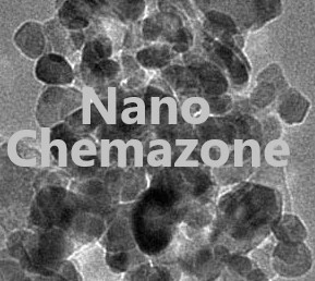
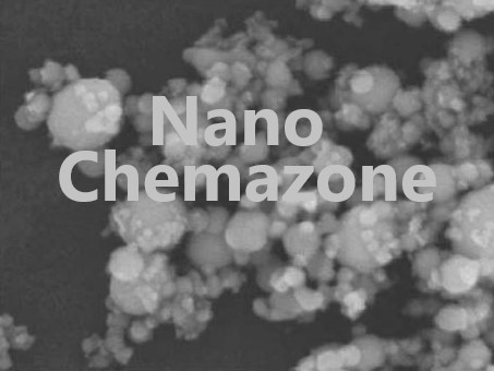
Tungsten Carbide (WC) Nanopowder/Nanoparticles
Purity: 99.99%, Size: 55 nm
Storage Condition:
Tungsten carbide nanoparticles should be sealed in vacuum and stored in cool and dry room. It should not be exposure to air and avoid stress.
Applications:
Tungsten carbide nanoparticles is a hard material, corrosion resistant, and waer resistant material. It is used in cutting tools, mining tolls, and
chipless forming tools. It is also used in coatings such as corrosion-resistant coatings, wear-resistance coatings, and erosion-resistant coatings.
In order to enhance hardness, strength, and wear resistance tungsten carbide nanoparticles is used in nano-compsites. It is used in producing
super fine horniness alloy and high capability nano-crystalline. It is also used as in catalysis as petrochemical cracking catalyst.