Applications of Sputtering Targets;
Film deposition is accomplished using sputtering targets. A technique for sputtering thin films is called "deposition made by sputter targets," which entails eroding material from a "target" source onto a "substrate" like a silicon wafer.
Etching of the target is done using semiconductor sputtering targets. When selectivity is not an issue and a high degree of etching anisotropy is required, sputter etching is the method of choice.
By removing the target material through etching, sputter targets are also utilized for investigation.
In secondary ion spectroscopy (SIMS), one example is when the target material is sputtered at a steady pace. When the target shatters,
Mass spectrometry measures the concentration and identity of sputtered atoms. The target material's composition may be ascertained and even very low concentrations of contaminants can be found with the aid of the sputtering target.
There is also an application area for sputtering targets in space. One type of space weathering that alters the chemical and physical characteristics of airless worlds like the Moon and asteroids is sputtering.
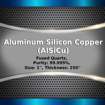
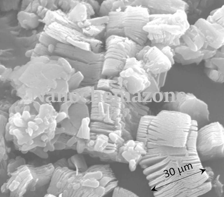
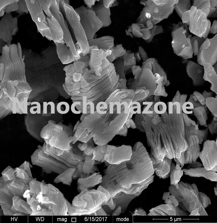
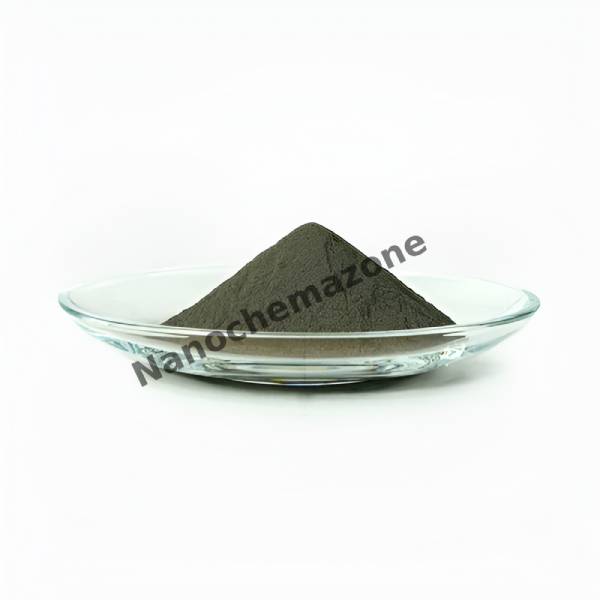
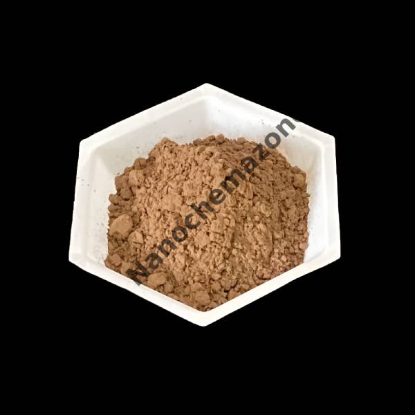
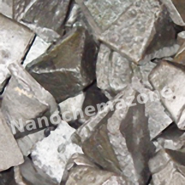
Aluminum has a good strength to weight ratio. Aluminum plating is the best material to use on cars, trucks, and airplanes. To improve its structural qualities and overall performance, aluminum is typically alloyed with silicon and copper, among other elements.
When compared to aluminum silicon alloys, aluminum silicon copper alloys are well known for their exceptionally high strength. Aluminum silicon copper sputtering targets are ideal for usage in the transportation and aerospace industries due to their exceptional strength.
Sputtering targets made of aluminum silicon copper have superior casting and machining properties. This alloy has excellent corrosion resistance and weldability, which make it ideal for use in gas and oil pans, engine parts, and other commercial applications.
For semiconductor applications, aluminum silicon copper sputtering targets can also be employed. This alloy forms a homogeneous film due to its high purity.