25 grams/26 €
100 grams/53 €
500 grams/98 €
1000 grams/141 €
Please contact us for quotes on larger quantities !!!
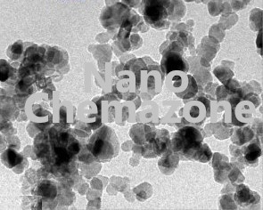
Silicon Dioxide (SiO2) Nanopowder/Nanoparticles
Purity: 96.3+%, Size: 18-35 nm, KH550 Coated
Technical Properties:
| Purity (%) |
96.3+ |
|
|
|
|
| Color |
white |
|
|
|
|
| Average Particle Size (nm) |
18-35 |
|
|
|
|
| Specific Surface Area (m2/g) |
150-550 |
|
|
|
|
| Bulk Density (g/cm3) |
<0.1 |
|
|
|
|
| True Density (g/cm3) |
2,2 |
|
|
|
|
| Elemental Analysis (%) |
SiO2 : KH550 |
Fe |
Ca |
Ti |
Na |
|
96.3 : 3-4 |
0.02 |
0.002 |
0.012 |
0.025 |
Chemical Properties:
Silicon dioxide nanoparticles coated with KH570-Silane coupling agent is super oleophilic, and hydrophilic. It is suitable for both oily and waterborne systems.
Applications:
Silicon dioxide nanoparticle is used as additive for plastics, rubber, ceramics, porcelain, glass, adhesives, fibers, and many other products. It is added to concrete
and construction composites as strengthening filler. It has also applications in biomedical field such as drug delivery and theranostics. Silicon dioxide is also used
in environmental protection products. Silane KH-550 is used to increase mechanical, electrical, anti-aging, and water resistance properties for organic polymers and
inorganic fillers.