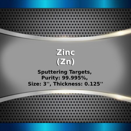
Applications of Sputtering Targets;
- Sputtering targets is used for film deposition. The deposition made by sputter targets is a method of depositing thin films by sputtering
that involves eroding material from a "target" source onto a "substrate" such as a silicon wafer.
- Semiconductor sputtering targets is used to etch the target. Sputter etching is chosen in cases where a high degree of etching anisotropy
is needed and selectivity is not a concern.
- Sputter targets is also used for analysis by etching away the target material.
One of the example occurs in secondary ion spectroscopy (SIMS), where the target sample is sputtered at a constant rate. As the target is sputtered,
the concentration and identity of sputtered atoms are measured using mass spectrometry. By helping of the sputtering target, the composition of the
target material can be determined and even extremely low concentrations of impurities are detected.
Sputtering target has also application area in space. Sputtering is one of the forms of space weathering, a process that changes the physical and
chemical properties of airless bodies, such as asteroids and the Moon.
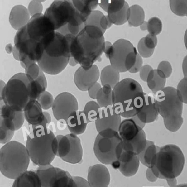
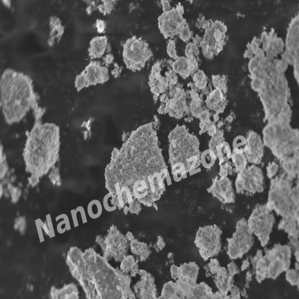
Erbium oxide with a chemical formula of Er
2O
3 is an oxide of erbium metal.
The applications of erbium oxide are varied due to their electrical, optical and photoluminescence properties. Nanoscale materials doped with Er
+3 are
of much interest because they have special particle-size-dependent optical and electrical properties. Erbium oxide doped nanoparticle materials can be
dispersed in glass or plastic for display purposes, such as display monitors. The spectroscopy of Er
+3 electronic transitions in host crystals lattices of
nanoparticles combined with ultrasonically formed geometries in aqueous solution of carbon nanotubes is of great interest for synthesis of
photoluminescence nanoparticles in ‘green’ chemistry. Erbium oxide is among the most important rare earth metals used in biomedicine. Erbium oxides
are also used as gate dielectrics in semiconductor devices since it has a high dielectric constant (10-14) and a large band gap. Erbium is sometimes used
as a coloring for glasses and erbium oxide can also be used as a burnable neutron poison for nuclear fuel. Erbium oxide films obtained by sputtering can
be used for their photoluminescence effect.