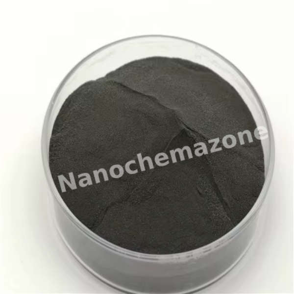
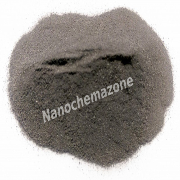
Manganese (Mn) Sputtering Targets, Purity: 99.95%, Size: 4”, Thickness: 0.250”

$537.00

Product 

Manganese (Mn) Sputtering Targets, Purity: 99.95%, Size: 4'', Thickness: 0.250''

CAS No.

 7439-96-5

Appearance

Powder

Purity

≥99%,  ≥99.9%,  ≥95%

(Other purities are also available)

APS

 N/A (Size Can be customized), Ask for other available size ranges.

Ingredient

N/A

Molecular Weight

54.93804 g/mol

Melting Point

 1,246 °C

Boiling Point

 2,061 °C

Density

 7.21 g/cm³

Product Codes

NCZ-1947K

Manganese (Mn) Sputtering Targets, Purity: 99.95%, Size: 4”, Thickness: 0.125”

$537.00

Product 

Manganese (Mn) Sputtering Targets, Purity: 99.95%, Size: 4'', Thickness: 0.125''

CAS No.

 7439-96-5

Appearance

Powder

Purity

≥99%,  ≥99.9%,  ≥95%

(Other purities are also available)

APS

 N/A (Size Can be customized), Ask for other available size ranges.

Ingredient

N/A

Molecular Weight

54.93804 g/mol

Melting Point

 1,246 °C

Boiling Point

 2,061 °C

Density

 7.21 g/cm³

Product Codes

NCZ-1948K

Ytterbium Oxide (Yb2O3) Sputtering Targets, Purity: 99.99%, Size: 2”, Thickness: 0.125”

$538.00

Applications of Sputtering Targets;

  • Sputtering targets is used for film deposition. The deposition made by sputter targets is a method of depositing thin films by sputtering that involves eroding material from a "target" source onto a "substrate" such as  a silicon wafer.
  • Semiconductor sputtering targets is used to etch the target. Sputter etching is chosen in cases where a high degree of etching anisotropy is needed and selectivity is not a concern.
  • Sputter targets is also used for analysis by etching away the target material.
One of the example occurs in secondary ion spectroscopy (SIMS), where the target sample is sputtered at a constant rate. As the target is sputtered, the concentration and identity of sputtered atoms are measured using mass spectrometry. By helping of the sputtering target, the composition of the target material can be determined and even extremely low concentrations of impurities are detected. Sputtering target has also application area in space. Sputtering is one of the forms of space weathering, a process that changes the physical and chemical properties of airless bodies, such as asteroids and the Moon.

Silicon Nitride (Si3N4) Sputtering Targets, Purity: 99.5%, Size: 2”, Thickness: 0.250”, Dark Gray to Black

$538.00

Product 

Silicon Nitride (Si3N4) Sputtering Targets, Purity: 99.5%, Size: 2'', Thickness: 0.250'', Dark Gray to Black

CAS No.

 12033-89-5

Appearance

Powder

Purity

≥99%,  ≥99.9%,  ≥95%

(Other purities are also available)

APS

N/A  (Size Can be customized), Ask for other available size ranges.

Ingredient

N/A

Molecular Weight

 140.28 g/mol

Melting Point

 ~1900 °C

Boiling Point

N/A

Density

~3.2 g/cm³

Product Codes

NCZ-1699K

Lanthanum Titanate (LaTiO3) Sputtering Targets, Purity: 99.9%, Size: 1”, Thickness: 0.125”

$538.00

Product 

Lanthanum Titanate (LaTiO3) Sputtering Targets, Purity: 99.9%, Size: 1'', Thickness: 0.125''

CAS No.

12031‑47‑9 (specific to size) or 12201‑04‑6 (general LaTiO₃)

Appearance

Powder

Purity

≥99%,  ≥99.9%,  ≥95%

(Other purities are also available)

APS

<5 µm (Size Can be customized), Ask for other available size ranges.

Ingredient

N/A

Molecular Weight

 234.77 g/mol (exact ~234.839 g/mol)

Melting Point

 Approx. 2,200 °C

Boiling Point

N/A

Density

N/A

Product Codes

NCZ-2094K

Indium (In) Sputtering Targets, Purity: 99.99%, Size: 4”, Thickness: 0.125”

$538.00

Product 

Indium (In) Sputtering Targets, Purity: 99.99%, Size: 4'', Thickness: 0.125''

CAS No.

 7440-74-6

Appearance

Powder

Purity

≥99%,  ≥99.9%,  ≥95%

(Other purities are also available)

APS

 N/A (Size Can be customized), Ask for other available size ranges.

Ingredient

N/A

Molecular Weight

114.82 g/mol

Melting Point

 156.6 °C

Boiling Point

 2,072 °C

Density

 7.31 g/cm³

Product Codes

NCZ-2223K

99.95% Manganese (Mn) Micron Powder (-320 Mesh), 1kg

$539.00
Product 99.95% Manganese (Mn) Micron Powder (-320 Mesh), 1kg
CAS No. 7439-96-5
Appearance Gray to silvery metallic
Purity ≥99%,  ≥99.9%,  ≥95%(Other purities are also available)
APS 44µm  (Size Can be customized),  Ask for other available size range.
Ingredient Mn
Molecular Weight 54.94 g/mol
Melting Point 1246 °C
Boiling Point 2061 °C
Density 2.1–3.5 g/cm³
Product Codes NCZ-233I

Titanium Aluminum Carbonitride (Ti3AlCN) MAX Phase Micron-Powder, 1-40um, 10g

$539.00
Product Titanium Aluminum Carbonitride (Ti3AlCN) MAX Phase Micron-Powder, 1-40um, 10g
CAS No. N/A
Appearance Dark grey to black
Purity ≥99%,  ≥99.9%,  ≥95%(Other purities are also available)
APS 1-40um (Size Can be customized),  Ask for other available size range.
Ingredient Ti3AlCN
Molecular Weight 196.60 g/mol
Melting Point N/A
Boiling Point N/A
Density N/A
Product Codes NCZ-572I
 

Vanadium Aluminum Carbide (V4AlC3) MAX Phase Micron-Powder

Price range: $539.00 through $1,089.00
Select options This product has multiple variants. The options may be chosen on the product page
Product Vanadium Aluminum Carbide (V4AlC3) MAX Phase Micron-Powder
CAS No. 1019635-34-7
Appearance Dark gray to black
Purity ≥99%,  ≥99.9%,  ≥95%(Other purities are also available)
APS 40μm (Size Can be customized),  Ask for other available size range.
Ingredient V4AlC3
Molecular Weight 266.78 g/mol
Melting Point N/A
Boiling Point N/A
Density 5.24 g/cm³
Product Codes NCZ-593I

Zinc Selenide Quantum Dots (ZnSe/ZnS QD) 420 nm

Price range: $540.00 through $1,275.00
Select options This product has multiple variants. The options may be chosen on the product page
APPLICATIONS Due to their distinct qualities, ZnSe QDs are utilized in:
  • Light emmiting diodes (LEDs),
  • Photocatalysts,
  • Solar cells,
  • Biological markers,
  • Scintillators,
  • Sensors.

Magnesium Fluoride (MgF2) Sputtering Targets, Purity: 99.9%, Size: 2”, Thickness: 0.250′

$540.00

Applications of Sputtering Targets;

Film deposition is accomplished using sputtering targets. A technique for sputtering thin films is called "deposition made by sputter targets," which entails eroding material from a "target" source onto a "substrate" like a silicon wafer. Etching of the target is done using semiconductor sputtering targets. When selectivity is not an issue and a high degree of etching anisotropy is required, sputter etching is the method of choice. By removing the target material through etching, sputter targets are also utilized for investigation. In secondary ion spectroscopy (SIMS), one example is when the target material is sputtered at a steady pace. Mass spectrometry is used to quantify the concentration and identity of spewed atoms as the target is sputtered.

By helping of the sputtering target, the composition of the target material may be evaluated and even extremely tiny amounts of contaminants are recognized.

There is also an application area for sputtering targets in space. One type of space weathering that alters the chemical and physical characteristics of airless worlds like the Moon and asteroids is sputtering.

Tungsten (W) Sputtering Targets, Purity: 99.95%, Size: 6”, Thickness: 0.250”

$540.00

Applications of Sputtering Targets;

Film deposition is accomplished using sputtering targets. A technique for sputtering thin films is called "deposition made by sputter targets," which entails eroding material from a "target" source onto a "substrate" like a silicon wafer. Etching of the target is done using semiconductor sputtering targets. When selectivity is not an issue and a high degree of etching anisotropy is required, sputter etching is the method of choice. By removing the target material through etching, sputter targets are also utilized for investigation. In secondary ion spectroscopy (SIMS), one example is when the target material is sputtered at a steady pace. Mass spectrometry is used to quantify the concentration and identity of spewed atoms as the target is sputtered.

The target material's composition may be ascertained and even very low concentrations of contaminants can be found with the aid of the sputtering target.

There is also an application area for sputtering targets in space. One type of space weathering that alters the chemical and physical characteristics of airless worlds like the Moon and asteroids is sputtering.

Vanadium (V) Sputtering Targets, Purity: 99.5%, Size: 8”, Thickness: 0.250”

$540.00

Applications of Sputtering Targets;

Film deposition is accomplished using sputtering targets. A technique for sputtering thin films is called "deposition made by sputter targets," which entails eroding material from a "target" source onto a "substrate" like a silicon wafer. Etching of the target is done using semiconductor sputtering targets. When selectivity is not an issue and a high degree of etching anisotropy is required, sputter etching is the method of choice. By removing the target material through etching, sputter targets are also utilized for investigation. In secondary ion spectroscopy (SIMS), one example is when the target material is sputtered at a steady pace. Mass spectrometry is used to quantify the concentration and identity of spewed atoms as the target is sputtered.

The target material's composition may be ascertained and even very low concentrations of contaminants can be found with the aid of the sputtering target.

There is also an application area for sputtering targets in space. One type of space weathering that alters the chemical and physical characteristics of airless worlds like the Moon and asteroids is sputtering.

Vanadium Oxide (V2O5) Sputtering Targets, Purity: 99.9%, Size: 3”, Thickness: 0.125”

$540.00

Product 

Vanadium Oxide (V2O5) Sputtering Targets, Purity: 99.9%, Size: 3'', Thickness: 0.125''

CAS No.

1314‑62‑1

Appearance

Powder

Purity

≥99%,  ≥99.9%,  ≥95%

(Other purities are also available)

APS

N/A  (Size Can be customized), Ask for other available size ranges.

Ingredient

N/A

Molecular Weight

181.88 g/mol

Melting Point

690 °C

Boiling Point

~1750 °C

Density

~3.35 g/cm³

Product Codes

NCZ-1539K

Tungsten (W) Sputtering Targets, elastomer, Purity: 99.95%, Size: 2”, Thickness: 0.125”

$540.00

Product 

Tungsten (W) Sputtering Targets, elastomer, Purity: 99.95%, Size: 2'', Thickness: 0.125''

CAS No.

7440-33-7

Appearance

Powder

Purity

≥99%,  ≥99.9%,  ≥95%

(Other purities are also available)

APS

N/A  (Size Can be customized), Ask for other available size ranges.

Ingredient

N/A

Molecular Weight

 183.84 g/mol

Melting Point

3422 °C

Boiling Point

 5555 °C

Density

19.25 g/cm³

Product Codes

NCZ-1584K

Niobium Oxide (Nb2O5) Sputtering Targets, indium, Purity: 99.5%, Size: 4”, Thickness: 0.125”

$540.00

Product 

Niobium Oxide (Nb2O5) Sputtering Targets, indium, Purity: 99.5%, Size: 4'', Thickness: 0.125''

CAS No.

1313-96-8

Appearance

Powder

Purity

≥99%,  ≥99.9%,  ≥95%

(Other purities are also available)

APS

N/A (Size Can be customized), Ask for other available size ranges.

Ingredient

N/A

Molecular Weight

 265.81 g/mol

Melting Point

~1512 °C

Boiling Point

N/A

Density

 4.6 – 4.9 g/cm³

Product Codes

NCZ-1802K

Magnesium carbonate whisker(MgCO3, ≥98%, D=1-2um, L=20-60um) (125665)

$540.00
Select options This product has multiple variants. The options may be chosen on the product page
Magnesium carbonate whisker(MgCO3, ≥98%, D=1-2um, L=20-60um) (125665)


MgO

≥47.3%

Length-Diameter ratio

20-50

Length/um

20-60

Diameter/um

1-2

 
Product Codes- NCZ-2752K

Vanadium Oxide (V2O5) Sputtering Targets, Purity: 99.9%, Size: 4”, Thickness: 0.250”

$541.00

Applications of Sputtering Targets;

Film deposition is accomplished using sputtering targets. A technique for sputtering thin films is called "deposition made by sputter targets," which entails eroding material from a "target" source onto a "substrate" like a silicon wafer. Etching of the target is done using semiconductor sputtering targets. When selectivity is not an issue and a high degree of etching anisotropy is required, sputter etching is the method of choice. By removing the target material through etching, sputter targets are also utilized for investigation. In secondary ion spectroscopy (SIMS), one example is when the target material is sputtered at a steady pace. Mass spectrometry is used to quantify the concentration and identity of spewed atoms as the target is sputtered.

The target material's composition may be ascertained and even very low concentrations of contaminants can be found with the aid of the sputtering target.

There is also an application area for sputtering targets in space. One type of space weathering that alters the chemical and physical characteristics of airless worlds like the Moon and asteroids is sputtering.

Lithium Nickel Cobalt Oxide (LiNi(1-x)CoxO2) Sputtering Targets, Purity: 99.9%, Size: 2”, Thickness: 0.125”

$542.00

Applications of Sputtering Targets;

Film deposition is accomplished using sputtering targets. A technique for sputtering thin films is called "deposition made by sputter targets," which entails eroding material from a "target" source onto a "substrate" like a silicon wafer. Etching of the target is done using semiconductor sputtering targets. When selectivity is not an issue and a high degree of etching anisotropy is required, sputter etching is the method of choice. By removing the target material through etching, sputter targets are also utilized for investigation. In secondary ion spectroscopy (SIMS), one example is when the target material is sputtered at a steady pace. Mass spectrometry is used to quantify the concentration and identity of spewed atoms as the target is sputtered.

By helping of the sputtering target, the composition of the target material may be evaluated and even extremely tiny amounts of contaminants are recognized.

There is also an application area for sputtering targets in space. One type of space weathering that alters the chemical and physical characteristics of airless worlds like the Moon and asteroids is sputtering.

Formula LiCoO2 represents the chemical compound lithium cobalt oxide. A crystalline solid that is dark blue or bluish-gray in color, lithium cobalt oxide is frequently utilized in the positive electrodes of lithium-ion batteries.

Lithium Niobate (LiNbO3) Sputtering Targets, Purity: 99.9%, Size: 2”, Thickness: 0.250”

$542.00

Applications of Sputtering Targets;

Film deposition is accomplished using sputtering targets. A technique for sputtering thin films is called "deposition made by sputter targets," which entails eroding material from a "target" source onto a "substrate" like a silicon wafer. Etching of the target is done using semiconductor sputtering targets. When selectivity is not an issue and a high degree of etching anisotropy is required, sputter etching is the method of choice. By removing the target material through etching, sputter targets are also utilized for investigation. In secondary ion spectroscopy (SIMS), one example is when the target material is sputtered at a steady pace. Mass spectrometry is used to quantify the concentration and identity of spewed atoms as the target is sputtered.

By helping of the sputtering target, the composition of the target material may be evaluated and even extremely tiny amounts of contaminants are recognized.

There is also an application area for sputtering targets in space. One type of space weathering that alters the chemical and physical characteristics of airless worlds like the Moon and asteroids is sputtering.

Tin (Sn) Sputtering Targets, Purity: 99.99%, Size: 6”, Thickness: 0.250”

$542.00

Applications of Sputtering Targets;

Film deposition is accomplished using sputtering targets. A technique for sputtering thin films is called "deposition made by sputter targets," which entails eroding material from a "target" source onto a "substrate" like a silicon wafer. Etching of the target is done using semiconductor sputtering targets. When selectivity is not an issue and a high degree of etching anisotropy is required, sputter etching is the method of choice. By removing the target material through etching, sputter targets are also utilized for investigation. In secondary ion spectroscopy (SIMS), one example is when the target material is sputtered at a steady pace. Mass spectrometry is used to quantify the concentration and identity of spewed atoms as the target is sputtered.

The target material's composition may be ascertained and even very low concentrations of contaminants can be found with the aid of the sputtering target.

There is also an application area for sputtering targets in space. One type of space weathering that alters the chemical and physical characteristics of airless worlds like the Moon and asteroids is sputtering.

Tin Oxide (SnO2) Sputtering Targets, Purity: 99.99%, Size: 1”, Thickness: 0.125”

$542.00

Applications of Sputtering Targets;

Film deposition is accomplished using sputtering targets. A technique for sputtering thin films is called "deposition made by sputter targets," which entails eroding material from a "target" source onto a "substrate" like a silicon wafer. Etching of the target is done using semiconductor sputtering targets. When selectivity is not an issue and a high degree of etching anisotropy is required, sputter etching is the method of choice. By removing the target material through etching, sputter targets are also utilized for investigation. In secondary ion spectroscopy (SIMS), one example is when the target material is sputtered at a steady pace. Mass spectrometry is used to quantify the concentration and identity of spewed atoms as the target is sputtered.

Even very low quantities of contaminants can be detected with the aid of the sputtering target, allowing for the determination of the target material's composition.

Applications for sputtering targets are also found in space. One type of space weathering is sputtering, which modifies the chemical and physical characteristics of airless worlds like the Moon and asteroids.

Titanium Dioxide (TiO2) Sputtering Targets, Purity: 99.9%, Size: 4”, Thickness: 0.250”, Grey to Black

$542.00

Applications of Sputtering Targets;

Film deposition is accomplished using sputtering targets. A technique for sputtering thin films is called "deposition made by sputter targets," which entails eroding material from a "target" source onto a "substrate" like a silicon wafer. Etching of the target is done using semiconductor sputtering targets. When selectivity is not an issue and a high degree of etching anisotropy is required, sputter etching is the method of choice. By removing the target material through etching, sputter targets are also utilized for investigation. In secondary ion spectroscopy (SIMS), one example is when the target material is sputtered at a steady pace. Mass spectrometry is used to quantify the concentration and identity of spewed atoms as the target is sputtered.

The target material's composition may be ascertained and even very low concentrations of contaminants can be found with the aid of the sputtering target.

There is also an application area for sputtering targets in space. One type of space weathering that alters the chemical and physical characteristics of airless worlds like the Moon and asteroids is sputtering.

Tetracalcium phosphate(Ca4(PO4)2O, Biomedicine grade, >98%) (204982)

$542.00
Select options This product has multiple variants. The options may be chosen on the product page

Product 

Tetracalcium phosphate(Ca4(PO4)2O, Biomedicine grade, >98%) (204982)

CAS No.

1306‑01‑0

Appearance

Powder

Purity

≥99%,  ≥99.9%,  ≥95%

(Other purities are also available)

APS

  <80um (Size Can be customized), Ask for other available size ranges.

Ingredient

N/A

Molecular Weight

~366.25 g/mol

Melting Point

Decomposes at ~1450 °C

Boiling Point

N/A

Density

 Not widely documented (but typical calcium phosphates range ~2.9–3.2 g/cm³)

Product Codes

NCZ-2612K

Indium Oxide (In2O3) Sputtering Targets, Purity: 99.99%, Size: 2”, Thickness: 0.125”

$543.00

Product 

Indium Oxide (In2O3) Sputtering Targets, Purity: 99.99%, Size: 2'', Thickness: 0.125''

CAS No.

 1312-43-2

Appearance

Powder

Purity

≥99%,  ≥99.9%,  ≥95%

(Other purities are also available)

APS

< 5 µm (Size Can be customized), Ask for other available size ranges.

Ingredient

N/A

Molecular Weight

 277.64 g/mol

Melting Point

 ~1,910 °C

Boiling Point

 3,000 °C(approx., decomposes)

Density

~7.18 g/cm³ (sintered form)

Product Codes

NCZ-2218K

High-Performance Copper Foil Rolls for Lithium Ion Battery, Size: 25 µm

Price range: $544.00 through $2,482.00
Select options This product has multiple variants. The options may be chosen on the product page
1 roll/544 € 5 rolls/2482 € Please contact us for quotes on larger quantities !!! High-Performance Copper Foil Rolls for Lithium Ion Battery

High-Performance Copper Foil Rolls for Lithium Ion Battery, Size: 25 µm

Price range: $544.00 through $2,482.00
Select options This product has multiple variants. The options may be chosen on the product page
1 roll/544 € 5 rolls/2482 € Please contact us for quotes on larger quantities !!! High-Performance Copper Foil Rolls for Lithium Ion Battery

Ytterbium Oxide (Yb2O3) Sputtering Targets, Purity: 99.9%, Size: 3”, Thickness: 0.125”

$544.00

Applications of Sputtering Targets;

  • Sputtering targets is used for film deposition. The deposition made by sputter targets is a method of depositing thin films by sputtering that involves eroding material from a "target" source onto a "substrate" such as  a silicon wafer.
  • Semiconductor sputtering targets is used to etch the target. Sputter etching is chosen in cases where a high degree of etching anisotropy is needed and selectivity is not a concern.
  • Sputter targets is also used for analysis by etching away the target material.
One of the example occurs in secondary ion spectroscopy (SIMS), where the target sample is sputtered at a constant rate. As the target is sputtered, the concentration and identity of sputtered atoms are measured using mass spectrometry. By helping of the sputtering target, the composition of the target material can be determined and even extremely low concentrations of impurities are detected. Sputtering target has also application area in space. Sputtering is one of the forms of space weathering, a process that changes the physical and chemical properties of airless bodies, such as asteroids and the Moon.

Molybdenum Disulfide (MoS2) Sputtering Targets, Purity: 99.9%, Size: 2”, Thickness: 0.250”

$544.00

Product 

Molybdenum Disulfide (MoS2) Sputtering Targets, Purity: 99.9%, Size: 2'', Thickness: 0.250''

CAS No.

 1317-33-5

Appearance

Powder

Purity

≥99%,  ≥99.9%,  ≥95%

(Other purities are also available)

APS

 N/A (Size Can be customized), Ask for other available size ranges.

Ingredient

N/A

Molecular Weight

 160.07 g/mol

Melting Point

 ~1185 °C

Boiling Point

 ~4500 °C

Density

 ~5.06 g/cm³

Product Codes

NCZ-1916K

Lanthanum Calcium Manganate (La0.7Ca0.3MnO3) Sputtering Targets, Purity: 99.9%, Size: 1”, Thickness: 0.125”

$544.00

Product 

Lanthanum Calcium Manganate (La0.7Ca0.3MnO3) Sputtering Targets, Purity: 99.9%, Size: 1'', Thickness: 0.125''

CAS No.

123273‑09‑6

Appearance

Powder

Purity

≥99%,  ≥99.9%,  ≥95%

(Other purities are also available)

APS

N/A (Size Can be customized), Ask for other available size ranges.

Ingredient

N/A

Molecular Weight

 ~313.9 g/mol

Melting Point

 ~1,550 °C (approximate; ceramic decomposition likely above)

Boiling Point

N/A

Density

 ~5.3 g/cm³ @ room temp

Product Codes

NCZ-2158K

Calcium Manganate (CaMnO3) Sputtering Targets, Purity: 99.9%, Size: 2”, Thickness: 0.125”

$544.00

Product 

Calcium Manganate (CaMnO3) Sputtering Targets, Purity: 99.9%, Size: 2'', Thickness: 0.125''

CAS No.

12058-85-6

Appearance

Powder

Purity

≥99%,  ≥99.9%,  ≥95%

(Other purities are also available)

APS

 N/A (Size Can be customized), Ask for other available size ranges.

Ingredient

N/A

Molecular Weight

157.87 g/mol

Melting Point

 Approx. 1400 °C (decomposes)

Boiling Point

N/A

Density

 ~4.7 g/cm³

Product Codes

NCZ-2361K

Silicon Carbide Wafer (SiC-4H) – 4H, Size: 4”, Thickness: 350 μm, Mechanical Grade, 4H Area: 80%

Price range: $545.00 through $2,514.00
Select options This product has multiple variants. The options may be chosen on the product page
1 piece/495 € 5 pieces/2280 €               Please contact us for quotes on larger quantities !!!

Silicon Carbide Wafer (SiC-4H) - 4H

Size: 4'', Thickness: 350 μm, 4H Area: 80%

Technical Properties:

Quality  Mechanical Grade
Size (inch)  4”
Thickness (μm)  350
Ra  ≤1
4H area  80%
Orientation  4°±0.5°
Resistivity   0.015-0.03
TTV  ≤25
Bow  ≤30
Warp  ≤45
OF Length  32.5±2
IF Length  18±2

Fields of Application for Silicon Carbide (SiC-4H)- 4H Wafer

Silicon carbide (SiC) is a rare compound of silicon and carbon which is synthetically produced. Silicon carbide (SiC) wafer has great electrical properties and excellent thermal properties. Silicon carbide (SiC) wafer has low thermal expansion. Silicon carbide (SiC) wafer has superior hardness properties. Silicon carbide (SiC) wafer performs well at high temperatures. Also, silicon carbide (SiC) wafer has high resistance to corrosion, erosion and oxidation. In addition to, silicon carbide (SiC) wafer is also more shiny than either diamonds or cubic zirconia. While Silicon carbide (SiC-4H) - 4H wafer has superior electronic properties, silicon carbide (SiC-6H) – 6H wafer is most easily prepared and best studied.
  • Silicon carbide (SiC) wafer is used for hybrid and electric vehicles.
  • Silicon carbide (SiC) wafer is used for green energy generation.
  • Silicon carbide (SiC) wafer is used for LEDs.
  • Silicon carbide (SiC) wafer is used for many other emerging markets.

Silicon Carbide Wafer (SiC-6H) – 6H , Size: 2”, Thickness: 350 μm, Dummy Grade, Usable Area: 95%

Price range: $545.00 through $2,415.00
Select options This product has multiple variants. The options may be chosen on the product page
1 piece/495 € 5 pieces/2190 €                           Please contact us for quotes on larger quantities !!!

Silicon Carbide Wafer (SiC-6H) - 6H

Size: 2'', Thickness: 350 μm, Usable Area: 95%

Technical Properties:

Quality  Dummy Grade
Size (inch)  2”
Thickness (μm)  350
Ra  ≤1
Usable Area  95%
Orientation  <0001>±0.5°
Resistivity   0.02 ~0.1 Ω·cm
TTV  ≤25
Bow  ≤30
Warp  ≤45
OF Length  15.9±1.7
IF Length  8±1.7

Fields of Application for Silicon Carbide (SiC-6H)- 6H Wafer

Silicon carbide (SiC) is a rare compound of silicon and carbon which is synthetically produced. Silicon carbide (SiC) wafer has great electrical properties and excellent thermal properties. Silicon carbide (SiC) wafer has low thermal expansion. Silicon carbide (SiC) wafer has superior hardness properties. Silicon carbide (SiC) wafer performs well at high temperatures. Also, silicon carbide (SiC) wafer has high resistance to corrosion, erosion and oxidation. In addition to, silicon carbide (SiC) wafer is also more shiny than either diamonds or cubic zirconia. Silicon carbide (SiC) crystals have unique physical and electronic properties. Silicon Carbide based devices have been used for short wavelength opto-electronic, high temperature, radiation resistant applications.  The high-power and high-frequency electronic devices made with SiC are superior to Si and GaAs based devices.  Below are some popular applications of SiC substrates. SiC based devices have low lattice mismatch with III-nitride epitaxial layers.  They have high thermal conductivity and can be used for the monitoring of combustion processes and for all sorts of UV-detection.  SiC-based semiconductor devices can work under very hostile environments, such as high temperature, high power, and high radiation conditions. SiC is used for the fabrication of very high-voltage and high-power devices such as diodes, power transistors, and high power microwave devices. Compared to conventional Si-devices, SiC-based power devices have faster switching speed higher voltages, lower parasitic resistances, smaller size, less cooling required due to high-temperature capability. While Silicon carbide (SiC-6H) - 6H wafer has superior electronic properties, silicon carbide (SiC-6H) – 6H wafer is most easily prepared and best studied.
  • Silicon carbide (SiC) wafer is used for hybrid and electric vehicles.
  • Silicon carbide (SiC) wafer is used for green energy generation.
  • Silicon carbide (SiC) wafer is used for LEDs.
  • Silicon carbide (SiC) wafer is used for many other emerging markets.

Indium Phosphide Quantum (InP/ZnS QD) Dots 600 nm

Price range: $545.00 through $1,280.00
Select options This product has multiple variants. The options may be chosen on the product page
APPLICATIONS InPQDs are employed in because of their electrical and optical characteristics in:
  • Light emitting diodes (LEDs),
  • Biomedical applications like bioimaging,
  • Electronic devices,
  • Solar cells.

Calcium Manganate (CaMnO3) Sputtering Targets, Purity: 99.9%, Size: 4”, Thickness: 0.125”

$545.00

Applications of Sputtering Targets;

Film deposition is accomplished using sputtering targets. A technique for sputtering thin films is called "deposition made by sputter targets," which entails eroding material from a "target" source onto a "substrate" like a silicon wafer. Etching of the target is done using semiconductor sputtering targets. When selectivity is not an issue and a high degree of etching anisotropy is required, sputter etching is the method of choice. By removing the target material through etching, sputter targets are also utilized for investigation. In secondary ion spectroscopy (SIMS), one example is when the target material is sputtered at a steady pace. Mass spectrometry is used to quantify the concentration and identity of spewed atoms as the target is sputtered.

The target material's composition may be ascertained and even very low concentrations of contaminants can be found with the aid of the sputtering target.

There is also an application area for sputtering targets in space. One type of space weathering that alters the chemical and physical characteristics of airless worlds like the Moon and asteroids is sputtering.

Industrial Grade Graphene Oxides (97%, <2nm, diameter: 3~10um)

$545.00
Select options This product has multiple variants. The options may be chosen on the product page
$115/g $545/5g
Product Industrial Grade Graphene Oxides (97%, <2nm, diameter: 3~10um)
CAS No. 7782-42-5
Appearance Black powder
Purity ≥99%,  ≥99.9%,  ≥95%(Other purities are also available)
APS 3-10um (Size Can be customized),  Ask for other available size range.
Ingredient (CₓOyHz)
Molecular Weight 1106.96 g/mol
Melting Point N/A
Boiling Point N/A
Density 1.36 g/cm³
Product Codes NCZ-118G

Amino Modified Dendritic Large Pore Diameter Mesoporous Silica Solution/Powder

$545.00
Select options This product has multiple variants. The options may be chosen on the product page
Product Amino Modified Dendritic Large Pore Diameter Mesoporous Silica Solution/Powder
CAS No. 919-30-2
Appearance Clear to pale yellow
Purity ≥99%,  ≥99.9%,  ≥95%(Other purities are also available)
APS N/A
Ingredient C₉H₂₃NO₃Si
Molecular Weight 221.37 g/mol
Melting Point N/A
Boiling Point N/A
Density 2.0 g/cm³.
Product Codes NCZ-287I
 

Carboxyl Modified Dendritic Large Pore Diameter Mesoporous Silica

$545.00
Select options This product has multiple variants. The options may be chosen on the product page
Product Carboxyl Modified Dendritic Large Pore Diameter Mesoporous Silica
CAS No. 7440-21-3
Appearance White to off white
Purity ≥99%,  ≥99.9%,  ≥95%(Other purities are also available)
APS 100nm (Size Can be customized),  Ask for other available size range.
Ingredient SiO₂
Molecular Weight N/A
Melting Point N/A
Boiling Point N/A
Density 0.3–0.6 g/cm³
Product Codes NCZ-306I
 

High Purity 99.9wt% Hollow Mesoporous Silica Powder (Spherical)

Price range: $545.00 through $1,723.00
Select options This product has multiple variants. The options may be chosen on the product page
Product High Purity 99.9wt% Hollow Mesoporous Silica Powder (Spherical)
CAS No. 7631-86-9
Appearance White to off-white fine
Purity ≥99%,  ≥99.9%,  ≥95%(Other purities are also available)
APS 2-50nm (Size Can be customized),  Ask for other available size range.
Ingredient SiO₂
Molecular Weight 60.08 g/mol
Melting Point N/A
Boiling Point N/A
Density 2.2 g/cm³
Product Codes NCZ-402I
 

Large Pore Diameter Dendritic Mesoporous Silica Solution/Powder

$545.00
Select options This product has multiple variants. The options may be chosen on the product page
Product Large Pore Diameter Dendritic Mesoporous Silica Solution/Powder
CAS No. 7631-86-9
Appearance Fine white to off-white
Purity ≥99%,  ≥99.9%,  ≥95%(Other purities are also available)
APS 100nm (Size Can be customized),  Ask for other available size range.
Ingredient SiO₂
Molecular Weight N/A
Melting Point N/A
Boiling Point N/A
Density N/A
Product Codes NCZ-441I
 

Aluminum dihydrogen tripolyphosphate(AlH2P3O10·2H2O) (157885)

$545.00
Select options This product has multiple variants. The options may be chosen on the product page
Aluminum dihydrogen tripolyphosphate(AlH2P3O10·2H2O) (157885)

 CAS  17375-35-8

Project Guaranteed Values Examination result
Color White White powder
The PH value 3-5 5
Moisture % ≤2 1.5
Residue on sieve( 45um)                ≤0.5% 0.4
P2O5   % 60-70 61.5
Al2O3  % 20-30 26
AS ≤100ppm 90
Cd ≤100ppm 20
Cr ≤100ppm 15
Hg ≤10ppm 0.0005
Pb ≤200ppm 80
Product Codes- NCZ-2590K

TEMPO oxidized CNF

$545.00
Select options This product has multiple variants. The options may be chosen on the product page

Product 

TEMPO oxidized CNF

CAS No.

9004-34-6

Appearance

Powder

Purity

≥99%,  ≥99.9%,  ≥95%

(Other purities are also available)

APS

~3–10 nm (Size Can be customized), Ask for other available size ranges.

Ingredient

N/A

Molecular Weight

 Undefined – it's a polymer (but ~162.14 g/mol per glucose unit)

Melting Point

N/A

Boiling Point

N/A

Density

~1.3–1.5 g/cm³ (bulk powder form)

Product Codes

NCZ-2591K

Cellulose nanofiber(CNF) (252567) Gel TEMPO oxidized CNF

$545.00
Select options This product has multiple variants. The options may be chosen on the product page
Cellulose nanofiber(CNF) (252567) Gel TEMPO oxidized CNF
TEMPO oxidized CNF Grade Carboxyl group(mmol/g) Length (µm) Diameter (nm) Appearance Concentration (w/w %) Price($)
TO-CNF-PL2-Gel 1.0-1.3 0.8-5 <10 Transparent or semitransparent Hydrogel 1 545/500ml
TO-CNF-PL10-Gel 1.3-1.6 5-10 <15
TO-CNF-PL20-Gel 1.6-2.2 10-20 <20
Product Codes- NCZ-2592K

Cellulose nanofiber(CNF) (252567) Gel Cationic modified CNF

$545.00
Select options This product has multiple variants. The options may be chosen on the product page
Cellulose nanofiber(CNF) (252567) Gel Cationic modified CNF
Cationic modified CNF Grade Charge density(mmol/g) Length (µm) Diameter (nm) Appearance Concentration (w/w %) Price($)
C-CNF-PL5-Gel 1.3-1.6 1-10 <10 Transparent or semitransparent Hydrogel 1 545/500ml
C-CNF-PL10-Gel 1.0-1.3 10-20 <20
C-CNF-PL20-Gel 0.7-1.0 20-30 <30
Product Codes- NCZ-2593K

Cellulose nanofiber(CNF) (252567) Paste Original CNF (without modification)

$545.00
Select options This product has multiple variants. The options may be chosen on the product page
Cellulose nanofiber(CNF) (252567) Paste Original CNF (without modification)
Original CNF (without modification) Grade Length (µm) Diameter (nm) Appearance Concentration (w/w %) Price($)
UM-CNF-PL10-Paste 1-10 <10 White paste 1.0 545/500ml
UM-CNF-PL30-Paste 10-30 <15 2.0 545/500ml
Product Codes- NCZ-2594K  

Original CNF (without modification) UM-CNF-PL30-Paste

$545.00
Select options This product has multiple variants. The options may be chosen on the product page

Product 

Original CNF (without modification) UM-CNF-PL30-Paste

CAS No.

 9004-34-6 (same as cellulose)

Appearance

Powder

Purity

≥99%,  ≥99.9%,  ≥95%

(Other purities are also available)

APS

 5–20 nm diameter, length: 0.5–10 μm(Size Can be customized), Ask for other available size ranges.

Ingredient

N/A

Molecular Weight

 Not fixed (polymer) – repeat unit: 162.14 g/mol

Melting Point

 ❌ Nonethermal degradation starts ~240–260 °C

Boiling Point

N/A

Density

 ~1.3 – 1.6 g/cm³ (crystalline cellulose ~1.54 g/cm³)

Product Codes

NCZ-2595K

Original CNF (without modification)

$545.00
Select options This product has multiple variants. The options may be chosen on the product page

Product 

Original CNF (without modification)

CAS No.

 9004-34-6

Appearance

Powder

Purity

≥99%,  ≥99.9%,  ≥95%

(Other purities are also available)

APS

 ~5–20 nm diameter, length: 0.5–10 μm(Size Can be customized), Ask for other available size ranges.

Ingredient

N/A

Molecular Weight

Not fixed – polymer; per glucose unit: 162.14 g/mol

Melting Point

N/A

Boiling Point

N/A

Density

~1.3 – 1.6 g/cm³ (depends on crystallinity and form: gel, powder, film)

Product Codes

NCZ-2596K

Silk Fibroin (363619)

$545.00
Select options This product has multiple variants. The options may be chosen on the product page
Silk Fibroin (363619)
Items Specifications
Appearance White or grayish yellow powder
Total Nitrogen (%) ≥14.5
Weight loss on drying (%) ≤6.0
Residue on ignition (%) ≤4.0
pH value 5.0-7.0
   
Grade Particle diameter(µm) Price($/kg)
363619-1 40 445
363619-2 10 445
363619-3 5 445
363619-4 2 445
  Product Codes- NCZ-2629K

Cellulose nanofiber(CNF) (252567) Powder TEMPO oxidized CNF

$545.00
Select options This product has multiple variants. The options may be chosen on the product page
Cellulose nanofiber(CNF) (252567) Powder TEMPO oxidized CNF
TEMPO oxidized CNF Grade Carboxyl group(mmol/g) Length (µm) Diameter (nm) Appearance Concentration (w/w %) Price($)
TO-CNF-PL2-Powder 1.0-1.3 0.8-5 <10 Powder >92 545/10g
TO-CNF-PL10-Powder 1.3-1.6 5-10 <15
TO-CNF-PL20-Powder 1.6-2.2 10-20 <20
Product Codes- NCZ-2649K

N,O-Carboxymethyl Chitosan(from Mushroom, Water soluble) (336555)

$545.00
Select options This product has multiple variants. The options may be chosen on the product page
N,O-Carboxymethyl Chitosan(from Mushroom, Water soluble) (336555)
ANALYSIS SPECIFICATION
Characters/appearance White to light yellow powder
pH 7-8
Degree of Substitution 80%
Viscosity in 1% Acetic acid 10-80 cps
Mesh size/sieve analysis 100% pass 80 mesh
Loss on drying ≤8%
Total ash ≤ 2%
Heavy Metals As Pb Cd Hg Sum ≤ 2.0 ppm ≤ 1.0 ppm ≤ 0.5 ppm ≤ 0.5 ppm ≤ 20.0 ppm
Microbiological quality Total Plate Count Yeast & Mold E.Coli. Salmonella . <1000 cfu/g <100 cfu/g Negative Negative
    Product Codes- NCZ-2666K  

Aluminum Foam(Open Micropore, 1.6mm) (537636)

$545.00
Select options This product has multiple variants. The options may be chosen on the product page
Aluminum Foam(Open Micropore, 1.6mm) (537636)
  Primary Pore Size: 1.6mm Porosity: 85-90% Through Hole Rate: 50% Volume Density: 0.7g/cm3 Dimensions: per customer request   Product Codes- NCZ-2670K

Kish Graphite(85%) (368667)

$545.00
Select options This product has multiple variants. The options may be chosen on the product page
Kish Graphite(industrial grade, 80-90%) (371667)
  Kish Graphite is a byproduct of steel-making. The more modern steel-making processes do not result in the generation of Kish graphite, but in earlier times it was produced during the cooling of molten steel. It is obtained when carbon crystallizes from molten steel during the steel manufacturing process. It is used by hundreds of research groups to make graphene by mechanical exfoliation.  With preparation methods, the size of kish graphite is from mm to cm. As it is obtained by high temperature, the main applications include: as raw materials to synthesis the graphene, graphite intercalation compounds, and the fundamental research works such as the properties of graphite, large size graphite layer compounds.
Product Codes- NCZ-2717K

Magnesium (Mg) Sputtering Targets, Purity: 99.98%, Size: 8”, Thickness: 0.250”

$546.00

Applications of Sputtering Targets;

Film deposition is accomplished using sputtering targets. A technique for sputtering thin films is called "deposition made by sputter targets," which entails eroding material from a "target" source onto a "substrate" like a silicon wafer. Etching of the target is done using semiconductor sputtering targets. When etching anisotropy is high, sputter etching is the preferred method.

is required, and selectivity is unimportant. By removing the target material through etching, sputter targets are also utilized for investigation. In secondary ion spectroscopy (SIMS), one example is when the target material is sputtered at a steady pace. Mass spectrometry is used to quantify the concentration and identity of spewed atoms as the target is sputtered.

By helping of the sputtering target, the composition of the target material may be evaluated and even extremely tiny amounts of contaminants are recognized.

There is also an application area for sputtering targets in space. One type of space weathering that alters the chemical and physical characteristics of airless worlds like the Moon and asteroids is sputtering.

Magnesium Oxide (MgO) Sputtering Targets, Purity: 99.95%, Size: 5”, Thickness: 0.250”

$546.00

Applications of Sputtering Targets;

Film deposition is accomplished using sputtering targets. A technique for sputtering thin films is called "deposition made by sputter targets," which entails eroding material from a "target" source onto a "substrate" like a silicon wafer. Etching of the target is done using semiconductor sputtering targets. When selectivity is not an issue and a high degree of etching anisotropy is required, sputter etching is the method of choice. By removing the target material through etching, sputter targets are also utilized for investigation. In secondary ion spectroscopy (SIMS), one example is when the target material is sputtered at a steady pace. Mass spectrometry is used to quantify the concentration and identity of spewed atoms as the target is sputtered.

By helping of the sputtering target, the composition of the target material may be evaluated and even extremely tiny amounts of contaminants are recognized.

There is also an application area for sputtering targets in space. One type of space weathering that alters the chemical and physical characteristics of airless worlds like the Moon and asteroids is sputtering.

Tin (Sn) Sputtering Targets, Purity: 99.99%, Size: 4”, Thickness: 0.250”

$546.00

Applications of Sputtering Targets;

Film deposition is accomplished using sputtering targets. A technique for sputtering thin films is called "deposition made by sputter targets," which entails eroding material from a "target" source onto a "substrate" like a silicon wafer. Etching of the target is done using semiconductor sputtering targets. When selectivity is not an issue and a high degree of etching anisotropy is required, sputter etching is the method of choice. By removing the target material through etching, sputter targets are also utilized for investigation. In secondary ion spectroscopy (SIMS), one example is when the target material is sputtered at a steady pace. Mass spectrometry is used to quantify the concentration and identity of spewed atoms as the target is sputtered.

The target material's composition may be ascertained and even very low concentrations of contaminants can be found with the aid of the sputtering target.

There is also an application area for sputtering targets in space. One type of space weathering that alters the chemical and physical characteristics of airless worlds like the Moon and asteroids is sputtering.

Tungsten Disulfide (WS2) Sputtering Targets, indium, Purity: 99.9%, Size: 2”, Thickness: 0.125”

$546.00

Applications of Sputtering Targets;

Film deposition is accomplished using sputtering targets. A technique for sputtering thin films is called "deposition made by sputter targets," which entails eroding material from a "target" source onto a "substrate" like a silicon wafer. Etching of the target is done using semiconductor sputtering targets. When selectivity is not an issue and a high degree of etching anisotropy is required, sputter etching is the method of choice. By removing the target material through etching, sputter targets are also utilized for investigation. In secondary ion spectroscopy (SIMS), one example is when the target material is sputtered at a steady pace. Mass spectrometry is used to quantify the concentration and identity of spewed atoms as the target is sputtered.

The target material's composition may be ascertained and even very low concentrations of contaminants can be found with the aid of the sputtering target.

There is also an application area for sputtering targets in space. One type of space weathering that alters the chemical and physical characteristics of airless worlds like the Moon and asteroids is sputtering.

Tungsten Disulfide (WS2) Sputtering Targets, Purity: 99.9%, Size: 4”, Thickness: 0.250”

$546.00

Applications of Sputtering Targets;

Film deposition is accomplished using sputtering targets. A technique for sputtering thin films is called "deposition made by sputter targets," which entails eroding material from a "target" source onto a "substrate" like a silicon wafer. Etching of the target is done using semiconductor sputtering targets. When selectivity is not an issue and a high degree of etching anisotropy is required, sputter etching is the method of choice. By removing the target material through etching, sputter targets are also utilized for investigation. In secondary ion spectroscopy (SIMS), one example is when the target material is sputtered at a steady pace. Mass spectrometry is used to quantify the concentration and identity of spewed atoms as the target is sputtered.

The target material's composition may be ascertained and even very low concentrations of contaminants can be found with the aid of the sputtering target.

There is also an application area for sputtering targets in space. One type of space weathering that alters the chemical and physical characteristics of airless worlds like the Moon and asteroids is sputtering.

Silicon Carbide Wafer (SiC-4H) – 4H, Size: 2”, Thickness: 350 μm, Testing Grade, 4H Area: 80%

Price range: $547.00 through $2,412.00
Select options This product has multiple variants. The options may be chosen on the product page
Silicon Carbide Wafer (SiC-4H) – 4H Size: 2” , Thickness: 350 μm, 4H Area: 80% Technical Properties: Quality  Testing Grade Size (inch)

Antimony Telluride (Sb2Te3) Sputtering Targets, Purity: 99.999%, Size: 1”, Thickness: 0.125”

$547.00

Applications of Sputtering Targets;

Film deposition is accomplished using sputtering targets. A technique for sputtering thin films is called "deposition made by sputter targets," which entails eroding material from a "target" source onto a "substrate" like a silicon wafer. Etching of the target is done using semiconductor sputtering targets. When selectivity is not an issue and a high degree of etching anisotropy is required, sputter etching is the method of choice. By removing the target material through etching, sputter targets are also utilized for investigation. In secondary ion spectroscopy (SIMS), one example is when the target material is sputtered at a steady pace. When the target shatters,

Mass spectrometry measures the concentration and identity of sputtered atoms. The target material's composition may be ascertained and even very low concentrations of contaminants can be found with the aid of the sputtering target.

There is also an application area for sputtering targets in space. One type of space weathering that alters the chemical and physical characteristics of airless worlds like the Moon and asteroids is sputtering.

The chemical formula for antimony telluride, an inorganic molecule, is Sb2Te3. It has a layered structure and is a grey crystalline solid. Layers are made of of

Weak van der Waals forces hold the two antimony atomic sheets and the three tellurium atomic sheets together.

Let's now examine the regions in which antimony telluride sputtering targets are used. Since thermoelectric devices can directly convert heat into electric energy, they have garnered a lot of interest for use as power generators, coolers, and thermal sensors or detectors. The power factor or the dimensionless figure of merit (ZT) of the materials are used to assess thermoelectric device performance. Tellurium antimony (Sb2Te3)

Bismuth Telluride (Bi2Te3) Sputtering Targets, Purity: 99.999%, Size: 1”, Thickness: 0.250”

$547.00

Applications of Sputtering Targets;

Film deposition is accomplished using sputtering targets. A technique for sputtering thin films is called "deposition made by sputter targets," which entails eroding material from a "target" source onto a "substrate" like a silicon wafer. Etching of the target is done using semiconductor sputtering targets. When selectivity is not an issue and a high degree of etching anisotropy is required, sputter etching is the method of choice. By removing the target material through etching, sputter targets are also utilized for investigation. In secondary ion spectroscopy (SIMS), one example is when the target material is sputtered at a steady pace. Mass spectrometry is used to quantify the concentration and identity of spewed atoms as the target is sputtered.