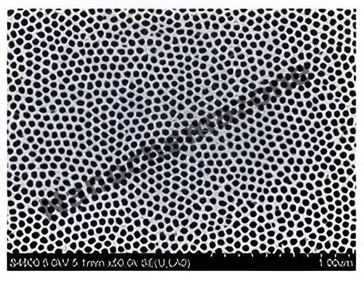
Applications of Sputtering Targets;
Film deposition is accomplished using sputtering targets. A technique for sputtering thin films is called "deposition made by sputter targets," which entails eroding material from a "target" source onto a "substrate" like a silicon wafer.
Etching of the target is done using semiconductor sputtering targets. When selectivity is not an issue and a high degree of etching anisotropy is required, sputter etching is the method of choice.
By removing the target material through etching, sputter targets are also utilized for investigation.
In secondary ion spectroscopy (SIMS), one example is when the target material is sputtered at a steady pace. When the target shatters,
Mass spectrometry measures the concentration and identity of sputtered atoms. The target material's composition may be ascertained and even very low concentrations of contaminants can be found with the aid of the sputtering target.
There is also an application area for sputtering targets in space. One type of space weathering that alters the chemical and physical characteristics of airless worlds like the Moon and asteroids is sputtering.
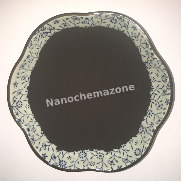
The metal bismuth is silvery with a hint of pink and is fragile. Both in air and water, it is stable. The thermal and electrical characteristics of bismuth are not good, yet
finds usage in the production of fusible alloys, a class of low-melting-point materials appropriate for a variety of functions, such as thermal fuses and solders. Because pure bismuth exhibits a high absorption of gamma rays, it can be used as a window or filter for these particles while allowing neutrons to pass through.
Due to high thermal conductivity, bimetal can be utilized in a wide range of applications, including heavy metal detection reference electrodes, devices that take use of substantial magneto-resistance, and thermoelectric conversion. Bi also has the intriguing characteristic of turning semi-metal films into semiconductors at a critical thickness of about 30 nm. These films can be deposited using a variety of methods, including laser heat evaporation, RF and DC sputtering, and pulsed deposition. Furthermore, it is significant to note that various authors have reported that the crystalline structure and morphology of Bi coatings deposited through physical vapor deposition (PVD) techniques depend on the deposition parameters, including the substrate's temperature, the potential applied to the target, the energy of the ion beam, and the rate at which energy is released during the ion beam bombardment that deposits the films. Positive pulses applied between the substrate and the target during DC sputtering can modify these parameters, improving the mechanical and density characteristics of the film.