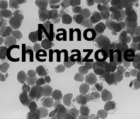
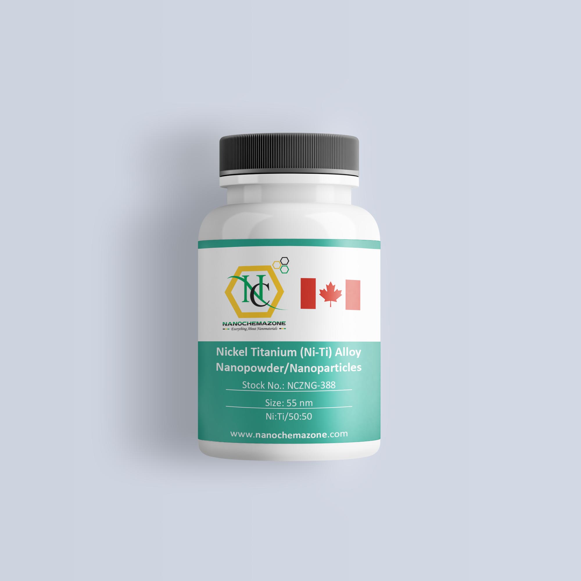
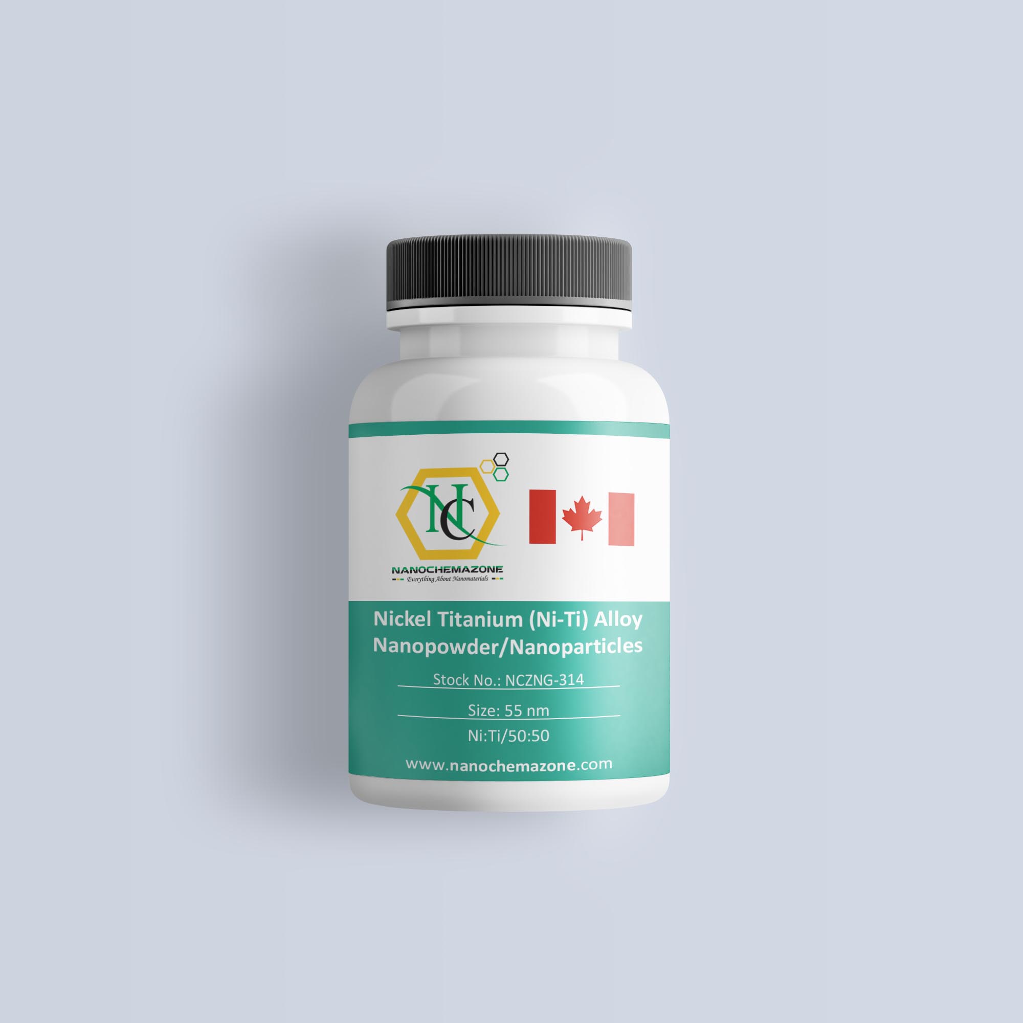
Nickel Titanium (Ni-Ti) Alloy Nanopowder/Nanoparticles
Size: 55 nm, Ni:Ti/50:50
Technical Properties:
| Alloy Ratio (Ni-Ti) |
50-50 |
|
|
|
|
| Average Particle Size (nm) |
55 |
|
|
|
|
| Elemental Analysis |
Ni-Ti |
Fe |
Cu |
Cr |
Others |
|
≥99.9 |
≤0.025 |
≤0.02 |
≤0.018 |
≤0.01 |
Properties, Storage and Cautions:
Ni-Ti alloy nanoparticles are highly reactive, therefore it should be handled with care and rapid moves, vibrations should be avoided.
The powder should be kept away from sunlight, any kind of heating, moisture and impacts. Coagulation of the particles is a serious
problem, so, the powder should be sealed under vacuum and should be kept in cool and dry conditions. Air contact should be avoided.
Applications:
Ni-Ti alloy materials show high elasticity and shape memory property. They can be used in heat engines, sensors, biomedical applications, actuators etc.