Tin (Sn) Sputtering Targets, Purity: 99.99%, Size: 2”, Thickness: 0.125”

$155.00

Product 

Tin (Sn) Sputtering Targets, Purity: 99.99%, Size: 2'', Thickness: 0.125''

CAS No.

7440-31-5

Appearance

Powder

Purity

≥99%,  ≥99.9%,  ≥95%

(Other purities are also available)

APS

N/A  (Size Can be customized), Ask for other available size ranges.

Ingredient

N/A

Molecular Weight

118.71 g/mol

Melting Point

231.93 °C

Boiling Point

2602 °C

Density

~7.31 g/cm³

Product Codes

NCZ-1644K

Iron (Fe) Sputtering Targets, Purity: 99.9%, Size: 2”, Thickness: 0.250”

$155.00

Product 

Iron (Fe) Sputtering Targets, Purity: 99.9%, Size: 2'', Thickness: 0.250''

CAS No.

 7439-89-6

Appearance

Powder

Purity

≥99%,  ≥99.9%,  ≥95%

(Other purities are also available)

APS

 N/A (Size Can be customized), Ask for other available size ranges.

Ingredient

N/A

Molecular Weight

 55.85 g/mol

Melting Point

 1538 °C

Boiling Point

 2862 °C

Density

 7.87 g/cm³

Product Codes

NCZ-2186K

Germanium (Ge) Sputtering Targets, Purity: 99.999%, Size: 1”, Thickness: 0.250”

$155.00

Product 

Germanium (Ge) Sputtering Targets, Purity: 99.999%, Size: 1'', Thickness: 0.250''

CAS No.

7440-56-4

Appearance

Powder

Purity

≥99%,  ≥99.9%,  ≥95%

(Other purities are also available)

APS

 N/A (Size Can be customized), Ask for other available size ranges.

Ingredient

N/A

Molecular Weight

 72.63 g/mol

Melting Point

 938.3 °C

Boiling Point

2,833 °C

Density

 5.32 g/cm³

Product Codes

NCZ-2242K

Plant dyes (526534)

$155.00
Plant dyes (526534) Plant dyes are extracted from raw materials such as flowers, shells, fruits, leaves and so on through multiple processes, powdering-extracting-ultrasonic processing-concentrating-air drying. Plant dyes can be used for cotton, linen, silk and wool dyeing. They have no side effects on our body. With natural color, well texture and pleasant fragrance, the dyed fabrics are the best choice for high grade garments. . Application Dosage: 0.5~5%(o.w.f), different usage according to color deep requirement
  1. Dyeing for cotton fabrics:
(1) Modification processing: natural modifier dosage is 1-2 times weights of cotton fabric, 95°C/30min ----washing----dyeing (2) Dyeing processing: 95°C/60min(pH 3-4) ----washing----soaping (soaping agent 5g/L, boiling 1-2min) ----washing----drying
  1. Dyeing for wool and silk fabrics:
Adopt acid- boiling dyeing for both wool and silk fabric. Adjust pH with glacial acetic acid. pH for dyeing wool fabric is 4. pH for silk fabric is 5.  
Grades Form Dye color Dyed fabric color Storage condition
Natural 0001 solid Dark red Rose madder room temperature
Natural 0002 solid Black(yellow) Yellowish brown room temperature
Natural 0003 solid Orange Bright yellow room temperature
Natural 0004 solid Blue Dark blue room temperature
Natural 0005 solid Black(red) Light brown room temperature
Natural 0006 solid Reddish brown Reddish brown room temperature
Natural 0007 solid Dark purple Cameo brown room temperature
Natural 0008 solid Dark yellow Watermelon red room temperature
Natural 0009 solid Nigger-brown Greenish yellow room temperature
Natural 0010 solid Grey Dove-gray room temperature
Natural 0011 solid Blue Indigo room temperature
Natural 0012 solid Olive green Olive green room temperature
Natural 0013 solid Brown Brown room temperature
Natural 0014 solid Tea color Green-tea color room temperature
Natural 0015 solid Brown Persimmon red room temperature
Natural 0016 solid Yellow Wooden yellow room temperature
Natural 0017 solid Pale brown Grey room temperature
Natural 0018 solid Pale brown Black room temperature
Natural 0019 solid Brown Locust Beige room temperature
Natural 0020 solid Brown Khaki room temperature
Natural 0021 solid dark green Green room temperature
   
Product Codes- NCZ-2791K

Copper Nickel (Cu-Ni) Alloy Nanopowder/Nanoparticles, Size: < 80 nm

Price range: $156.00 through $277.00
Select options This product has multiple variants. The options may be chosen on the product page

Copper Nickel (Cu-Ni) Alloy Nanopowder/Nanoparticles

Size: < 80 nm

Technical Properties:

Alloy Ratio (Cu-Ni) 50-50
Average Particle Size (nm) 80

Properties, Storage and Cautions:

Cu-Ni alloy nanoparticles are highly reactive, therefore it should be handled with care and rapid moves, vibrations should be avoided. The powder should be kept away from sunlight, any kind of heating, moisture and impacts. Coagulation of the particles is a serious problem, so, the powder should be sealed under vacuum and should be kept in cool and dry conditions. Air contact should be avoided.

Applications:

Cu-Ni alloy is known with its good machinability and resistance to corrosion. It is used in heat exchangers, fittings, pumps, cooling systems, power plants, coins, mechanical and electrical equipment, bullet jackets etc

Copper (Cu) Nanopowder/Nanoparticles, Purity: 99.95%, Size: 80 nm, Metal Basis

Price range: $156.00 through $278.00
Select options This product has multiple variants. The options may be chosen on the product page

Copper (Cu) Nanopowder/Nanoparticles

Purity: 99.95%, Size: 80 nm, Metal Basis

Technical Properties:

Bulk Density (g/cm3) 0,22
True Density (g/cm3) 8,9
Color warm copper brown
Shape spherical
Crystal Structure cubic
Average Particle Size (nm) 80
Specific Surface Area (m2/g) 5,0-5,8
Elemental Analysis Cu Fe Ni Others
99.95 0.006 0.005 0.002

Erbium Oxide (Er2O3) Sputtering Targets, Purity: 99.99%, Size: 3”, Thickness: 0.125”

$156.00
Select options This product has multiple variants. The options may be chosen on the product page

Applications of Sputtering Targets;

  • Sputtering targets is used for film deposition. The deposition made by sputter targets is a method of depositing thin films by sputtering that involves eroding material from a "target" source onto a "substrate" such as  a silicon wafer.
  • Semiconductor sputtering targets is used to etch the target. Sputter etching is chosen in cases where a high degree of etching anisotropy is needed and selectivity is not a concern.
  • Sputter targets is also used for analysis by etching away the target material.
One of the example occurs in secondary ion spectroscopy (SIMS), where the target sample is sputtered at a constant rate. As the target is sputtered, the concentration and identity of sputtered atoms are measured using mass spectrometry. By helping of the sputtering target, the composition of the target material can be determined and even extremely low concentrations of impurities are detected. Sputtering target has also application area in space. Sputtering is one of the forms of space weathering, a process that changes the physical and chemical properties of airless bodies, such as asteroids and the Moon. Erbium oxide with a chemical formula of Er2Ois an oxide of erbium metal. The applications of erbium oxide are varied due to their electrical, optical and photoluminescence properties. Nanoscale materials doped with Er+3 are of much interest because they have special particle-size-dependent optical and electrical properties. Erbium oxide doped nanoparticle materials can be dispersed in glass or plastic for display purposes, such as display monitors. The spectroscopy of Er+3 electronic transitions in host crystals lattices of nanoparticles combined with ultrasonically formed geometries in aqueous solution of carbon nanotubes is of great interest for synthesis of photoluminescence nanoparticles in ‘green’ chemistry. Erbium oxide is among the most important rare earth metals used in biomedicine. Erbium oxides are also used as gate dielectrics in semiconductor devices since it has a high dielectric constant (10-14) and a large band gap. Erbium is sometimes used as a coloring for glasses and erbium oxide can also be used as a burnable neutron poison for nuclear fuel. Erbium oxide films obtained by sputtering can be used for their photoluminescence effect.

Aluminum Silicon (AlSi) Sputtering Targets, Purity: 99.999%, Size: 3”, Thickness: 0.125”

$156.00

Applications of Sputtering Targets;

Film deposition is accomplished using sputtering targets. A technique for sputtering thin films is called "deposition made by sputter targets," which entails eroding material from a "target" source onto a "substrate" like a silicon wafer. Etching of the target is done using semiconductor sputtering targets. When selectivity is not an issue and a high degree of etching anisotropy is required, sputter etching is the method of choice. By removing the target material through etching, sputter targets are also utilized for investigation. In secondary ion spectroscopy (SIMS), one example is when the target material is sputtered at a steady pace. When the target shatters,

Mass spectrometry measures the concentration and identity of sputtered atoms. The target material's composition may be ascertained and even very low concentrations of contaminants can be found with the aid of the sputtering target.

There is also an application area for sputtering targets in space. One type of space weathering that alters the chemical and physical characteristics of airless worlds like the Moon and asteroids is sputtering.

Erbium Oxide (Er2O3) Sputtering Targets, Purity: 99.99%, Size: 3”, Thickness: 0.125”

$156.00

Applications of Sputtering Targets;

Film deposition is accomplished using sputtering targets. A technique for sputtering thin films is called "deposition made by sputter targets," which entails eroding material from a "target" source onto a "substrate" like a silicon wafer. Etching of the target is done using semiconductor sputtering targets. When selectivity is not an issue and a high degree of etching anisotropy is required, sputter etching is the method of choice. By removing the target material through etching, sputter targets are also utilized for investigation. In secondary ion spectroscopy (SIMS), one example is when the target material is sputtered at a steady pace. Mass spectrometry is used to quantify the concentration and identity of spewed atoms as the target is sputtered.

The target material's composition may be ascertained and even very low concentrations of contaminants can be found with the aid of the sputtering target.

There is also an application area for sputtering targets in space. One type of space weathering that alters the chemical and physical characteristics of airless worlds like the Moon and asteroids is sputtering.

Germanium (Ge) Sputtering Targets, indium, Purity: 99.999%, Size: 3”, Thickness: 0.125”

$156.00

Applications of Sputtering Targets;

Film deposition is accomplished using sputtering targets. A technique for sputtering thin films is called "deposition made by sputter targets," which entails eroding material from a "target" source onto a "substrate" like a silicon wafer. Etching of the target is done using semiconductor sputtering targets. When selectivity is not an issue and a high degree of etching anisotropy is required, sputter etching is the method of choice. By removing the target material through etching, sputter targets are also utilized for investigation. In secondary ion spectroscopy (SIMS), one example is when the target material is sputtered at a steady pace. Mass spectrometry is used to quantify the concentration and identity of spewed atoms as the target is sputtered.

The target material's composition may be ascertained and even very low concentrations of contaminants can be found with the aid of the sputtering target.

There is also an application area for sputtering targets in space. One type of space weathering that alters the chemical and physical characteristics of airless worlds like the Moon and asteroids is sputtering.

Iron (Fe) Sputtering Targets, Purity: 99.99%, Size: 2”, Thickness: 0.250”

$156.00

Applications of Sputtering Targets;

Film deposition is accomplished using sputtering targets. A technique for sputtering thin films is called "deposition made by sputter targets," which entails eroding material from a "target" source onto a "substrate" like a silicon wafer. Etching of the target is done using semiconductor sputtering targets. When selectivity is not an issue and a high degree of etching anisotropy is required, sputter etching is the method of choice. By removing the target material through etching, sputter targets are also utilized for investigation. In secondary ion spectroscopy (SIMS), one example is when the target material is sputtered at a steady pace. Mass spectrometry is used to quantify the concentration and identity of spewed atoms as the target is sputtered.

The target material's composition may be ascertained and even very low concentrations of contaminants can be found with the aid of the sputtering target.

There is also an application area for sputtering targets in space. One type of space weathering that alters the chemical and physical characteristics of airless worlds like the Moon and asteroids is sputtering.

Magnesium (Mg) Sputtering Targets, Purity: 99.98%, Size: 1”, Thickness: 0.250”

$156.00

Product 

Magnesium (Mg) Sputtering Targets, Purity: 99.98%, Size: 1'', Thickness: 0.250''

CAS No.

7439-95-4

Appearance

Powder

Purity

≥99%,  ≥99.9%,  ≥95%

(Other purities are also available)

APS

 N/A (Size Can be customized), Ask for other available size ranges.

Ingredient

N/A

Molecular Weight

 24.305 g/mol

Melting Point

 650 °C

Boiling Point

 1,090 °C

Density

1.738 g/cm³

Product Codes

NCZ-2004K

Lead (Pb) Sputtering Targets, Purity: 99.99+%, Size: 1”, Thickness: 0.250”

$156.00

Product 

Lead (Pb) Sputtering Targets, Purity: 99.99+%, Size: 1'', Thickness: 0.250''

CAS No.

7439‑92‑1

Appearance

Powder

Purity

≥99%,  ≥99.9%,  ≥95%

(Other purities are also available)

APS

 N/A (Size Can be customized), Ask for other available size ranges.

Ingredient

N/A

Molecular Weight

 207.2 g/mol

Melting Point

~327.5 °C

Boiling Point

~1,740 °C

Density

 ~11.34 g/cm³

Product Codes

NCZ-2077K

Aluminum (Al) Sputtering Targets, Purity: 99.99%, Size: 3”, Thickness: 0.250”

$156.00

Product 

Aluminum (Al) Sputtering Targets, Purity: 99.99%, Size: 3'', Thickness: 0.250''

CAS No.

 7429-90-5

Appearance

Powder

Purity

≥99%,  ≥99.9%,  ≥95%

(Other purities are also available)

APS

N/A (Size Can be customized), Ask for other available size ranges.

Ingredient

N/A

Molecular Weight

 26.98 g/mol

Melting Point

 660.3 °C

Boiling Point

 2519 °C

Density

 2.70 g/cm³

Product Codes

NCZ-2575K

Chitosan hydrochloride(Water soluble) (234668)

$156.00
Select options This product has multiple variants. The options may be chosen on the product page

Product

Chitosan hydrochloride(Water soluble) (234668)

CAS No.

70694‑72‑3

Appearance

Powder

Purity

≥99%,  ≥99.9%,  ≥95%

(Other purities are also available)

APS

  N/A(Size Can be customized), Ask for other available size ranges.

Ingredient

N/A

Molecular Weight

Polymer; ~215 g/mol per unit; overall range: a few kDa to >1 MDa

Melting Point

N/A

Boiling Point

N/A

Density

~1.5 g/cm³

Product Codes

NCZ-2655K

Copper (Cu) Sputtering Targets, Purity: 99.999%, Size: 3”, Thickness: 0.125”

$157.00

Applications of Sputtering Targets;

Film deposition is accomplished using sputtering targets. A technique for sputtering thin films is called "deposition made by sputter targets," which entails eroding material from a "target" source onto a "substrate" like a silicon wafer. Etching of the target is done using semiconductor sputtering targets. When selectivity is not an issue and a high degree of etching anisotropy is required, sputter etching is the method of choice. By removing the target material through etching, sputter targets are also utilized for investigation. In secondary ion spectroscopy (SIMS), one example is when the target material is sputtered at a steady pace. Mass spectrometry is used to quantify the concentration and identity of spewed atoms as the target is sputtered.

The target material's composition may be ascertained and even very low concentrations of contaminants can be found with the aid of the sputtering target.

There is also an application area for sputtering targets in space. One type of space weathering that alters the chemical and physical characteristics of airless worlds like the Moon and asteroids is sputtering.

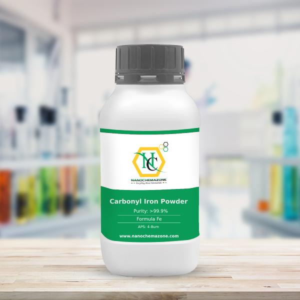
Carbonyl Iron Powder (Fe, 4-8um)

Price range: $157.00 through $233.00
Select options This product has multiple variants. The options may be chosen on the product page
$157/50g $233/100g

Product 

Carbonyl Iron Powder (Fe, 4-8um)

CAS No.

7439-89-6

Appearance

Powder

Purity

≥99%,  ≥99.9%,  ≥95%

(Other purities are also available)

APS

4–8 µm (microns) (Size Can be customized), Ask for other available size ranges.

Ingredient

N/A

Molecular Weight

55.845 g/mol

Melting Point

1538 °C

Boiling Point

2862 °C

Density

7.87 g/cm³

Product Codes

NCZ-1046K

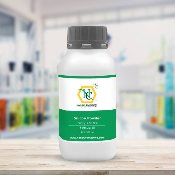
Silicon Nanopowder/ nanoparticles (Si, 99.9%, 500 nm)

Price range: $157.00 through $756.00
Select options This product has multiple variants. The options may be chosen on the product page
$157/100 g
$411/500g
$756/kg

Product 

Silicon Nanopowder/ nanoparticles (Si, 99.9%, 500 nm)

CAS No.

7440-21-3

Appearance

Powder

Purity

≥99%,  ≥99.9%,  ≥95%

(Other purities are also available)

APS

500 nm (Size Can be customized), Ask for other available size ranges.

Ingredient

N/A

Molecular Weight

28.0855 g/mol

Melting Point

1,414 °C

Boiling Point

3,265 °C

Density

~2.33 g/cm³

Product Codes

NCZ-1068K

Tin Sputtering Target Sn

Price range: $157.00 through $517.00
Select options This product has multiple variants. The options may be chosen on the product page
Product Tin Sputtering Target Sn
CAS No. N/A
Appearance Silvery Lustrous Gray, Metallic
Purity ≥99%,  ≥99.9%,  ≥95%(Other purities are also available)
APS N/A
Ingredient Sn
Molecular Weight 118.71 g/mol
Melting Point N/A
Boiling Point N/A
Density 7.365 g/cm³
Product Codes NCZ-143H

Nickel Iron (Ni-Fe) Sputtering Targets, Purity: 99.95%, Size: 1”, Thickness: 0.125”

$157.00

Product 

Nickel Iron (Ni-Fe) Sputtering Targets, Purity: 99.95%, Size: 1'', Thickness: 0.125''

CAS No.

N/A

Appearance

Powder

Purity

≥99%,  ≥99.9%,  ≥95%

(Other purities are also available)

APS

 N/A (Size Can be customized), Ask for other available size ranges.

Ingredient

N/A

Molecular Weight

 ~57.6 g/mol

Melting Point

 ~1,400 – 1,450 °C

Boiling Point

~2,730 – 2,750 °C

Density

 ~8.6 – 8.7 g/cm³

Product Codes

NCZ-1849K

Nickel Chromium (Ni-Cr) Sputtering Targets, Purity: 99.9%, Size: 1”, Thickness: 0.125”

$157.00

Product 

Nickel Chromium (Ni-Cr) Sputtering Targets, Purity: 99.9%, Size: 1'', Thickness: 0.125''

CAS No.

 11106-97-1

Appearance

Powder

Purity

≥99%,  ≥99.9%,  ≥95%

(Other purities are also available)

APS

 N/A (Size Can be customized), Ask for other available size ranges.

Ingredient

N/A

Molecular Weight

 ~110.69 g/mol

Melting Point

 ~1,400 °C

Boiling Point

 ~2,730–2,750 °C

Density

 ~8.4 – 8.5 g/cm³

Product Codes

NCZ-1861K

Nickel (Ni) Sputtering Targets, Purity: 99.99%, Size: 2”, Thickness: 0.125”

$157.00

Product 

Nickel (Ni) Sputtering Targets, Purity: 99.99%, Size: 2'', Thickness: 0.125''

CAS No.

7440-02-0

Appearance

Powder

Purity

≥99%,  ≥99.9%,  ≥95%

(Other purities are also available)

APS

 N/A (Size Can be customized), Ask for other available size ranges.

Ingredient

N/A

Molecular Weight

 58.69 g/mol

Melting Point

~1,453 °C

Boiling Point

~2,913 °C

Density

 8.90 g/cm³

Product Codes

NCZ-1891K

Multi Walled Carbon Nanotubes N-butanol Dispersion, 4 wt%, Purity: >96%, OD: 45-75 nm, Length 8-28 µm

Price range: $158.00 through $772.00
Select options This product has multiple variants. The options may be chosen on the product page

Applications:

MWCNTs have a variety of potential applications in different fields. These applications include midicine, mechanical, electric, chemical, energy and others. It can be applied in, 1-drug dilevery, 2-biosensors, 3-CNT composites, 4-catalysis, 5-nanoprobes, 6-hydrogen storage, 7-lithium battaries, 8-gas-discharge tubes, 9-flat panel display, 10-supercapacitor, 11-transistors, 12-solar cells, 13-photoluminescence, 14-tamplate  

Multi Walled Carbon Nanotubes Isopropanol Dispersion, 4 wt%, Purity: >96%, OD: 45-75 nm, Length 8-28 µm

Price range: $158.00 through $786.00
Select options This product has multiple variants. The options may be chosen on the product page

Applications:

MWCNTs have a variety of potential applications in different fields. These applications include midicine, mechanical, electric, chemical, energy and others. It can be applied in, 1-drug delivery, 2-biosensors, 3-CNT composites, 4-catalysis, 5-nanoprobes, 6-hydrogen storage, 7-lithium battaries, 8-gas-discharge tubes, 9-flat panel display, 10-supercapacitor, 11-transistors, 12-solar cells, 13-photoluminescence, 14-template

Nickel Vanadium (NiV) Sputtering Targets, Purity: 99.95%, Size: 1”, Thickness: 0.125”

$158.00

Applications of Sputtering Targets;

Film deposition is accomplished using sputtering targets. A technique for sputtering thin films is called "deposition made by sputter targets," which entails eroding material from a "target" source onto a "substrate" like a silicon wafer. Etching of the target is done using semiconductor sputtering targets. When selectivity is not an issue and a high degree of etching anisotropy is required, sputter etching is the method of choice. By removing the target material through etching, sputter targets are also utilized for investigation. In secondary ion spectroscopy (SIMS), one example is when the target material is sputtered at a steady pace. Mass spectrometry is used to quantify the concentration and identity of spewed atoms as the target is sputtered.

The target material's composition may be ascertained and even very low concentrations of contaminants can be found with the aid of the sputtering target.

There is also an application area for sputtering targets in space. One type of space weathering that alters the chemical and physical characteristics of airless worlds like the Moon and asteroids is sputtering.

Iron (Fe) Sputtering Targets, Purity: 99.9%, Size: 4”, Thickness: 0.125”

$158.00

Product 

Iron (Fe) Sputtering Targets, Purity: 99.9%, Size: 4'', Thickness: 0.125''

CAS No.

 7439-89-6

Appearance

Powder

Purity

≥99%,  ≥99.9%,  ≥95%

(Other purities are also available)

APS

 N/A (Size Can be customized), Ask for other available size ranges.

Ingredient

N/A

Molecular Weight

 55.85 g/mol

Melting Point

 1538 °C

Boiling Point

 2862 °C

Density

 7.87 g/cm³

Product Codes

NCZ-2180K

Platinum Oxide (PtO2) Nanopowder/Nanoparticles, Purity: 99.5+%, Size: <100 nm

Price range: $159.00 through $635.00
Select options This product has multiple variants. The options may be chosen on the product page
1 gram/140 € 5 grams/559 €                            
Please contact us for quotes on larger quantities !!!

Platinum Oxide (PtO2) Nanopowder/Nanoparticles

Purity: 99.5+%, Size: <100 nm

Iron (Fe) Sputtering Targets, Purity: 99.95%, Size: 4”, Thickness: 0.125”

$159.00

Applications of Sputtering Targets;

Film deposition is accomplished using sputtering targets. A technique for sputtering thin films is called "deposition made by sputter targets," which entails eroding material from a "target" source onto a "substrate" like a silicon wafer. Etching of the target is done using semiconductor sputtering targets. When selectivity is not an issue and a high degree of etching anisotropy is required, sputter etching is the method of choice. By removing the target material through etching, sputter targets are also utilized for investigation. In secondary ion spectroscopy (SIMS), one example is when the target material is sputtered at a steady pace. Mass spectrometry is used to quantify the concentration and identity of spewed atoms as the target is sputtered.

The target material's composition may be ascertained and even very low concentrations of contaminants can be found with the aid of the sputtering target.

There is also an application area for sputtering targets in space. One type of space weathering that alters the chemical and physical characteristics of airless worlds like the Moon and asteroids is sputtering.

Molybdenum (Mo) Sputtering Targets, Purity: 99.95%, Size: 1”, Thickness: 0.250”

$159.00

Product 

Molybdenum (Mo) Sputtering Targets, Purity: 99.95%, Size: 1'', Thickness: 0.250''

CAS No.

 7439-98-7

Appearance

Powder

Purity

≥99%,  ≥99.9%,  ≥95%

(Other purities are also available)

APS

 N/A (Size Can be customized), Ask for other available size ranges.

Ingredient

N/A

Molecular Weight

95.95 g/mol

Melting Point

 2623 °C

Boiling Point

 4639 °C

Density

10.28 g/cm³

Product Codes

NCZ-1940K

Aluminum Tab for Pouch Li-ion Cell, Width: 4 mm, Length: 57 mm

Price range: $160.00 through $594.00
Select options This product has multiple variants. The options may be chosen on the product page
100 pcs/128 € 250 pcs/265 € 500 pcs/475 €  Please contact us for quotes on larger quantities !!! 

Aluminum Tab for Pouch Li-ion Cell

Width: 4 mm, Length: 57 mm

Technical Properties:

Purity Aluminum 99.99%
Length 57 mm
Width 4 mm
Thickness 0.10 mm
Max. Loading Current 3A
Net Weight 60 mg/pcs

Applications:

4 mm Width Aluminum Tab as Positive Terminal for Pouch Li-ion Cell    

Thermoplastic Carbon Paste for Long-term Cell Degradation

Price range: $160.00 through $324.00
Select options This product has multiple variants. The options may be chosen on the product page

Application:

  • Perovskite Solar Cell

Thermoplastic Carbon Paste, Drying Temperature: <100 °C

Price range: $160.00 through $324.00
Select options This product has multiple variants. The options may be chosen on the product page

Application:

  • Perovskite Solar Cell

Hydrothermal Synthesis Autoclave Reactor with PTFE Lined Vessel 100 ml

$160.00
APPLICATIONs
  • Chemical synthesis
  • Synthesizing of nanoparticles
  • For cultured crystal growth
  • Polymerization reaction
  • Hydrothermal decomposition
  • Catalyst synthesis
  • Hydrothermal oxidation
  • Hydrothermal precipitation
  • Material Digester / digestion
  • Crystallization process
  • Dissolve of heavy metals, refractory material, organic chemicals etc.

5N (99.999%) Cesium Iodide (CsI) High Purity Powder

Price range: $161.00 through $623.00
Select options This product has multiple variants. The options may be chosen on the product page
Product 5N (99.999%) Cesium Iodide (CsI) High Purity Powder
CAS No. 7789-17-5
Appearance White
Purity ≥99%,  ≥99.9%,  ≥95%(Other purities are also available)
APS N/A
Ingredient CsI
Molecular Weight 259.81 g/mol
Melting Point N/A
Boiling Point N/A
Density 4.51 g/cm³
Product Codes NCZ-197I

99.99% 4N 30 nm Aluminum Oxide (Alumina) Al2O3 Powder, 500 g

$161.00
Product 99.99% 4N 30 nm Aluminum Oxide (Alumina) Al2O3 Powder, 500 g
CAS No. 1344-28-1
Appearance White
Purity ≥99%,  ≥99.9%,  ≥95%(Other purities are also available)
APS 30nm (Size Can be customized),  Ask for other available size range.
Ingredient Al2O3
Molecular Weight 101.96 g/mol
Melting Point N/A
Boiling Point N/A
Density 3.6 g/cm³
Product Codes NCZ-241I
 

99.99% 4N 50 nm Aluminum Oxide (Alumina) Al2O3 Powder with 180 – 260 m2/g SSA, 500 g

$161.00
Product 99.99% 4N 50 nm Aluminum Oxide (Alumina) Al2O3 Powder with 180 - 260 m2/g SSA, 500 g
CAS No. 1344-28-1
Appearance White
Purity ≥99%,  ≥99.9%,  ≥95%(Other purities are also available)
APS 50nm (Size Can be customized),  Ask for other available size range.
Ingredient Al2O3
Molecular Weight 101.96 g/mol
Melting Point N/A
Boiling Point N/A
Density 3.5 – 3.7 g/cm³
Product Codes NCZ-242I

99.99% 4N 50 nm Aluminum Oxide (Alumina) Al2O3 Powder, 500g

$161.00
Product 99.99% 4N 50 nm Aluminum Oxide (Alumina) Al2O3 Powder, 500g
CAS No. 1344-28-1
Appearance White
Purity ≥99%,  ≥99.9%,  ≥95%(Other purities are also available)
APS 50nm (Size Can be customized),  Ask for other available size range.
Ingredient Al2O3
Molecular Weight 101.96 g/mol
Melting Point N/A
Boiling Point N/A
Density 3.5 – 3.7 g/cm³
Product Codes NCZ-243I
 

99.99% 4N 50 nm Gamma Aluminum Oxide (Alumina) Al2O3 Powder, 500 g

$161.00
Product 99.99% 4N 50 nm Gamma Aluminum Oxide (Alumina) Al2O3 Powder, 500 g
CAS No. 1344-28-1
Appearance White to off-white fine
Purity ≥99%,  ≥99.9%,  ≥95%(Other purities are also available)
APS 50nm (Size Can be customized),  Ask for other available size range.
Ingredient Al2O3
Molecular Weight 101.96 g/mol
Melting Point N/A
Boiling Point N/A
Density 3.5 – 3.7 g/cm³
Product Codes NCZ-244I

Nickel (Ni) Sputtering Targets, Purity: 99.9%, Size: 2”, Thickness: 0.250”

$161.00

Product 

Nickel (Ni) Sputtering Targets, Purity: 99.9%, Size: 2'', Thickness: 0.250''

CAS No.

7440-02-0

Appearance

Powder

Purity

≥99%,  ≥99.9%,  ≥95%

(Other purities are also available)

APS

 N/A (Size Can be customized), Ask for other available size ranges.

Ingredient

N/A

Molecular Weight

 58.69 g/mol

Melting Point

~1,453 °C

Boiling Point

~2,732 – 2,914 °C

Density

 8.90 g/cm³

Product Codes

NCZ-1889K

Graphene on Quartz substrate (794508)

Price range: $161.00 through $1,345.00
Select options This product has multiple variants. The options may be chosen on the product page
Graphene on Quartz substrate (794508) Quartz parameter Thickness:1mm/2mm Transparent rate of quartz: >93% Graphene parameter and price
 
Substrate Layers Size Sheet Resistance(Ω/sq) Notes Price($/pc)
Quartz monolayer 10mm×10mm 300-500 monolayer coverage ≥95% 161
monolayer 15mm×15mm 300-500 monolayer coverage ≥95% 295
monolayer 20mm×20mm 300-500 monolayer coverage ≥95% 461
monolayer 50mm×50mm 300-500 monolayer coverage ≥95% 795
monolayer 100mm×100mm 300-500 monolayer coverage ≥95% 1175
double layer 10mm×10mm 200-300 225
double layer 15mm×15mm 200-300 461
double layer 20mm×20mm 200-300 645
double layer 50mm×50mm 200-300 1011
double layer 100mm×100mm 200-300 1345
Product Codes- NCZ-2588K  

Carbon Nanotubes Highly Conductive Tapes with Metal 8%, Thickness: 18 µm, Dia: 47 mm

$162.00
Select options This product has multiple variants. The options may be chosen on the product page
Applications:

Uses for Carbon Nanotubes Abundantly Conductive Materials for flexible electronics like tapes show promise. They are mechanically flexible, have high conductivity, and high intrinsic carrier mobility. They can be employed as the channel material in field-effect transistors (FETs) in flexible electronics. as electrodes as well. They can be utilized in many different flexible electronic products, including sensors, flexible solar cells, flexible displays, and flexible circuits.


Gallium Arsenide (GaAs) Wafers, Size: 2”, Thickness: 350±25 μm, Single Side Polished, EPI-ready

Price range: $162.00 through $3,108.00
Select options This product has multiple variants. The options may be chosen on the product page
Gallium Arsenide (GaAs) Wafer Size: 2”, Thickness: 350±25 μm, Single Side Polished Technical Properties: Quality  GaAs Materials  GaAs Size (inch)

Zinc (Zn) Sputtering Targets, Purity: 99.95%, Size: 2”, Thickness: 0.250”

$162.00

Applications of Sputtering Targets;

Film deposition is accomplished using sputtering targets. A technique for sputtering thin films is called "deposition made by sputter targets," which entails eroding material from a "target" source onto a "substrate" like a silicon wafer. Etching of the target is done using semiconductor sputtering targets. When selectivity is not an issue and a high degree of etching anisotropy is required, sputter etching is the method of choice. By removing the target material through etching, sputter targets are also utilized for investigation. In secondary ion spectroscopy (SIMS), one example is when the target material is sputtered at a steady pace. Mass spectrometry is used to quantify the concentration and identity of spewed atoms as the target is sputtered.

The target material's composition may be ascertained and even very low concentrations of contaminants can be found with the aid of the sputtering target.

There is also an application area for sputtering targets in space. One type of space weathering that alters the chemical and physical characteristics of airless worlds like the Moon and asteroids is sputtering.

Titanium Oxide Nanoparticles / Nanopowder 99.5%, Rutile, Silane Coated

Price range: $162.00 through $287.00
Select options This product has multiple variants. The options may be chosen on the product page
  $162/100g
$287/500g

Product 

Titanium Oxide Nanoparticles / Nanopowder 99.5%, Rutile, Silane Coated

CAS No.

 13463-67-7

Appearance

Powder

Purity

≥99%,  ≥99.9%,  ≥95%

(Other purities are also available)

APS

 10-30nm (Size Can be customized), Ask for other available size ranges.

Ingredient

N/A

Molecular Weight

79.87 g/mol

Melting Point

~1,843 °C

Boiling Point

~2,972 °C

Density

~4.23 g/cm³

Product Codes

NCZ-1196K

Tantalum Oxide (Ta2O5) Sputtering Target

Price range: $162.00 through $588.00
Select options This product has multiple variants. The options may be chosen on the product page

Product 

Tantalum Oxide (Ta2O5) Sputtering Target

CAS No.

13463-67-7

Appearance

Powder

Purity

≥99%,  ≥99.9%,  ≥95%

(Other purities are also available)

APS

 NA (Size Can be customized), Ask for other available size ranges.

Ingredient

N/A

Molecular Weight

79.87 g/mol

Melting Point

~1,843 °C

Boiling Point

~2,972 °C

Density

 ~4.23 g/cm³

Product Codes

NCZ-1326K

Molybdenum (Mo) Sputtering Targets, Purity: 99.95%, Size: 8”, Thickness: 0.125”

$162.00

Product 

Molybdenum (Mo) Sputtering Targets, Purity: 99.95%, Size: 8'', Thickness: 0.125''

CAS No.

 7439-98-7

Appearance

Powder

Purity

≥99%,  ≥99.9%,  ≥95%

(Other purities are also available)

APS

 N/A (Size Can be customized), Ask for other available size ranges.

Ingredient

N/A

Molecular Weight

95.95 g/mol

Melting Point

 2623 °C

Boiling Point

 4639 °C

Density

10.28 g/cm³

Product Codes

NCZ-1931K

Carbon (C) (Graphite) Sputtering Targets, Purity: 99.999%, Size: 2”, Thickness: 0.250”

$162.00

Product 

Carbon (C) (Graphite) Sputtering Targets, Purity: 99.999%, Size: 2'', Thickness: 0.250''

CAS No.

 7782‑42‑5

Appearance

Powder

Purity

≥99%,  ≥99.9%,  ≥95%

(Other purities are also available)

APS

 N/A (Size Can be customized), Ask for other available size ranges.

Ingredient

N/A

Molecular Weight

12.01 g/mol

Melting Point

~3,652 °C (no liquid phase)

Boiling Point

 ~4,200 °C

Density

 ~2.25 g/cm³

Product Codes

NCZ-2353K

Gallium Arsenide (GaAs) Wafers, Size: 2”, Thickness: 450±25 μm, Single Side Polished, EPI-ready, Dopant: Silicon (N Type)

Price range: $163.00 through $2,412.00
Select options This product has multiple variants. The options may be chosen on the product page
Gallium Arsenide (GaAs) Wafer Size: 2”, Single Side Polished, Thickness: 450± 25 μm, EPI-ready, Dopant: Silicon (N Type) Technical Properties:

Prime CZ-Si Wafer, Size: 8”, Orientation: (100), Boron Doped, Resistivity: 1-100 (ohm.cm), 1-Side Polished, Thickness: 725 ± 25 μm

Price range: $163.00 through $3,390.00
Select options This product has multiple variants. The options may be chosen on the product page
Prime CZ-Si Wafer Size: 8”, Orientation: (100), Boron Doped, 1-Side Polished, Thickness: 725 ± 25 μm Technical Properties: Quality Prime

Lithium Titanate (Li2TiO3) Sputtering Targets, Purity: 99.95%, Size: 1”, Thickness: 0.125”

$163.00

Applications of Sputtering Targets;

Film deposition is accomplished using sputtering targets. A technique for sputtering thin films is called "deposition made by sputter targets," which entails eroding material from a "target" source onto a "substrate" like a silicon wafer. Etching of the target is done using semiconductor sputtering targets. When selectivity is not an issue and a high degree of etching anisotropy is required, sputter etching is the method of choice. By removing the target material through etching, sputter targets are also utilized for investigation. In secondary ion spectroscopy (SIMS), one example is when the target material is sputtered at a steady pace. Mass spectrometry is used to quantify the concentration and identity of spewed atoms as the target is sputtered.

By helping of the sputtering target, the composition of the target material may be evaluated and even extremely tiny amounts of contaminants are recognized.

There is also an application area for sputtering targets in space. One type of space weathering that alters the chemical and physical characteristics of airless worlds like the Moon and asteroids is sputtering.

Molybdenum (Mo) Sputtering Targets, Purity: 99.95%, Size: 2”, Thickness: 0.125”

$163.00

Product 

Molybdenum (Mo) Sputtering Targets, Purity: 99.95%, Size: 2'', Thickness: 0.125''

CAS No.

 7439-98-7

Appearance

Powder

Purity

≥99%,  ≥99.9%,  ≥95%

(Other purities are also available)

APS

 N/A (Size Can be customized), Ask for other available size ranges.

Ingredient

N/A

Molecular Weight

95.95 g/mol

Melting Point

 2623 °C

Boiling Point

 4639 °C

Density

10.28 g/cm³

Product Codes

NCZ-1939K

Cobalt (Co) Sputtering Targets, Purity: 99.95%, Size: 3”, Thickness: 0.125”

$163.00

Product 

Cobalt (Co) Sputtering Targets, Purity: 99.95%, Size: 3'', Thickness: 0.125''

CAS No.

7440‑48‑4

Appearance

Powder

Purity

≥99%,  ≥99.9%,  ≥95%

(Other purities are also available)

APS

 N/A (Size Can be customized), Ask for other available size ranges.

Ingredient

N/A

Molecular Weight

58.93 g/mol (cobalt atomic weight)

Melting Point

~1,495 °C

Boiling Point

~2,870–2,927 °C

Density

~8.9 g/cm³

Product Codes

NCZ-2291K

Nickel (Ni) Sputtering Targets, Purity: 99.99%, Size: 2”, Thickness: 0.250”

$164.00

Applications of Sputtering Targets;

Film deposition is accomplished using sputtering targets. A technique for sputtering thin films is called "deposition made by sputter targets," which entails eroding material from a "target" source onto a "substrate" like a silicon wafer. Etching of the target is done using semiconductor sputtering targets. When selectivity is not an issue and a high degree of etching anisotropy is required, sputter etching is the method of choice. By removing the target material through etching, sputter targets are also utilized for investigation. In secondary ion spectroscopy (SIMS), one example is when the target material is sputtered at a steady pace. Mass spectrometry is used to quantify the concentration and identity of spewed atoms as the target is sputtered.

By helping of the sputtering target, the composition of the target material may be evaluated and even extremely tiny amounts of contaminants are recognized.

There is also an application area for sputtering targets in space. One type of space weathering that alters the chemical and physical characteristics of airless worlds like the Moon and asteroids is sputtering.

Nickel (Ni) Sputtering Targets, Purity: 99.99%, Size: 4”, Thickness: 0.125”

$164.00

Applications of Sputtering Targets;

Film deposition is accomplished using sputtering targets. A technique for sputtering thin films is called "deposition made by sputter targets," which entails eroding material from a "target" source onto a "substrate" like a silicon wafer. Etching of the target is done using semiconductor sputtering targets. When selectivity is not an issue and a high degree of etching anisotropy is required, sputter etching is the method of choice. By removing the target material through etching, sputter targets are also utilized for investigation. In secondary ion spectroscopy (SIMS), one example is when the target material is sputtered at a steady pace. Mass spectrometry is used to quantify the concentration and identity of spewed atoms as the target is sputtered.

By helping of the sputtering target, the composition of the target material may be evaluated and even extremely tiny amounts of contaminants are recognized.

There is also an application area for sputtering targets in space. One type of space weathering that alters the chemical and physical characteristics of airless worlds like the Moon and asteroids is sputtering.

Niobium (Nb) Sputtering Targets, Purity: 99.95% pure Ex Ta, Size: 2”, Thickness: 0.125”

$164.00

Applications of Sputtering Targets;

Film deposition is accomplished using sputtering targets. A technique for sputtering thin films is called "deposition made by sputter targets," which entails eroding material from a "target" source onto a "substrate" like a silicon wafer. Etching of the target is done using semiconductor sputtering targets. When selectivity is not an issue and a high degree of etching anisotropy is required, sputter etching is the method of choice. By removing the target material through etching, sputter targets are also utilized for investigation. In secondary ion spectroscopy (SIMS), one example is when the target material is sputtered at a steady pace. Mass spectrometry is used to quantify the concentration and identity of spewed atoms as the target is sputtered.

The target material's composition may be ascertained and even very low concentrations of contaminants can be found with the aid of the sputtering target.

There is also an application area for sputtering targets in space. One type of space weathering that alters the chemical and physical characteristics of airless worlds like the Moon and asteroids is sputtering.

Titanium (Ti) Sputtering Target

Price range: $164.00 through $504.00
Select options This product has multiple variants. The options may be chosen on the product page

Product 

Titanium (Ti) Sputtering Target

CAS No.

7440-32-6

Appearance

Powder

Purity

≥99%,  ≥99.9%,  ≥95%

(Other purities are also available)

APS

 NA (Size Can be customized), Ask for other available size ranges.

Ingredient

N/A

Molecular Weight

 47.87 g/mol

Melting Point

1,668 °C

Boiling Point

 3,287 °C

Density

4.506 g/cm³

Product Codes

NCZ-1363K

Lead (Pb) Sputtering Targets, Purity: 99.99+%, Size: 3”, Thickness: 0.125”

$164.00

Product 

Lead (Pb) Sputtering Targets, Purity: 99.99+%, Size: 2'', Thickness: 0.250''

CAS No.

7439‑92‑1

Appearance

Powder

Purity

≥99%,  ≥99.9%,  ≥95%

(Other purities are also available)

APS

 N/A (Size Can be customized), Ask for other available size ranges.

Ingredient

N/A

Molecular Weight

 207.2 g/mol

Melting Point

~327.5 °C

Boiling Point

~1,740 °C

Density

 ~11.34 g/cm³

Product Codes

NCZ-2075K

Tantalum (Ta) Nanopowder/Nanoparticles, High Purity: 99.995%, Size: 45-75 nm

Price range: $164.58 through $483.52
Select options This product has multiple variants. The options may be chosen on the product page
Tantalum (Ta) Nanopowder/Nanoparticles High Purity: 99.995%, Size: 45-75 nm Technical Properties: True Density (g/cm3) 16,7 Color black Shape spherical Tmelting (oC)

Fullerene-C70, Purity: 95%

Price range: $165.00 through $750.00
Select options This product has multiple variants. The options may be chosen on the product page
1 gram/148 € 5 grams/670 €                           
Please contact us for quotes on larger quantities !!!

Fullerene-C70

Purity: 95% 

Technical Properties:

Fullerene Compound Formula C70
Fullerene  Molecular Weight 840.77 g/mol
Fullerene  Purity 95%
Fullerene  Melting Point >280 °C
Fullerene  Appearance Black Powder
Fullerene  CAS 115383-22-7 

Applications:

1. Pharmaceutical: Diagnostic reagents, super drugs, cosmetics, nuclear magnetic resonance (NMR) with the developer. DNA affinity 2. Energy: Solar battery, fuel cell, secondary battery. 3. Industry: Wear resistant material, flame retardant materials, lubricants, polymer additives, high-performance membrane, catalyst, artificial diamond, hard alloy, electric viscous fluid, ink filters, high-performance coatings, fire retardant coatings, manufacturing bioactive materials , memory materials, embedded molecular and other characteristics, composite materials etc. 4. Information industry: Semiconductor record medium, magnetic materials, printing ink, toner, ink, paper special purposes. 5. Electronic parts: Superconducting semiconductor, diodes, transistors, inductor. 6. Optical materials, electronic camera, fluorescence display tube, nonlinear optical materials. 7. Environment: Gas adsorption, gas storage.  

Thermoplastic Carbon Paste, Drying Temperature: 120˚C for 10 minutes

Price range: $165.00 through $345.00
Select options This product has multiple variants. The options may be chosen on the product page

Applications:

  • Printed Electronics,
  • Touch Sensors,
  • Heaters,
  • Medical Devices