Applications of Sputtering Targets;
Film deposition is accomplished using sputtering targets. A technique for sputtering thin films is called "deposition made by sputter targets," which entails eroding material from a "target" source onto a "substrate" like a silicon wafer.
Etching of the target is done using semiconductor sputtering targets. When selectivity is not an issue and a high degree of etching anisotropy is required, sputter etching is the method of choice.
By removing the target material through etching, sputter targets are also utilized for investigation.
In secondary ion spectroscopy (SIMS), one example is when the target material is sputtered at a steady pace. When the target shatters,
Mass spectrometry measures the concentration and identity of sputtered atoms. The target material's composition may be ascertained and even very low concentrations of contaminants can be found with the aid of the sputtering target.
There is also an application area for sputtering targets in space. One type of space weathering that alters the chemical and physical characteristics of airless worlds like the Moon and asteroids is sputtering.
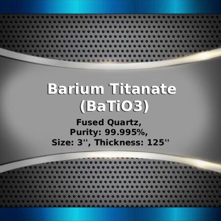
A Block S, Group 2, Period 6 element with an atomic weight of 137.27, barium has the atomic symbol Ba and atomic number 56. Barium is a mineral that an alkaline-earth metal member. Electronics can be plated using barium sputtering targets. Barium is beneficial for sputtering applications because of its good electrical characteristics. Barium sputtering targets can be utilized for semiconductors. Barium sputtering targets will work well for flat panel displays. Barium can be combined with other metals, such as titanium and strontium, to create alloys with more specialized qualities.