15 ml/250 €
30 ml/416 €
60 ml/720 €
120 ml/1200 €
Please contact us for quotes on larger quantities !!!
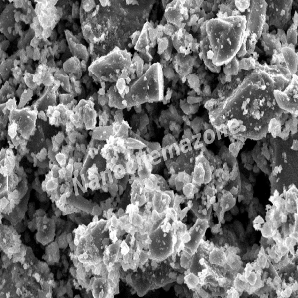
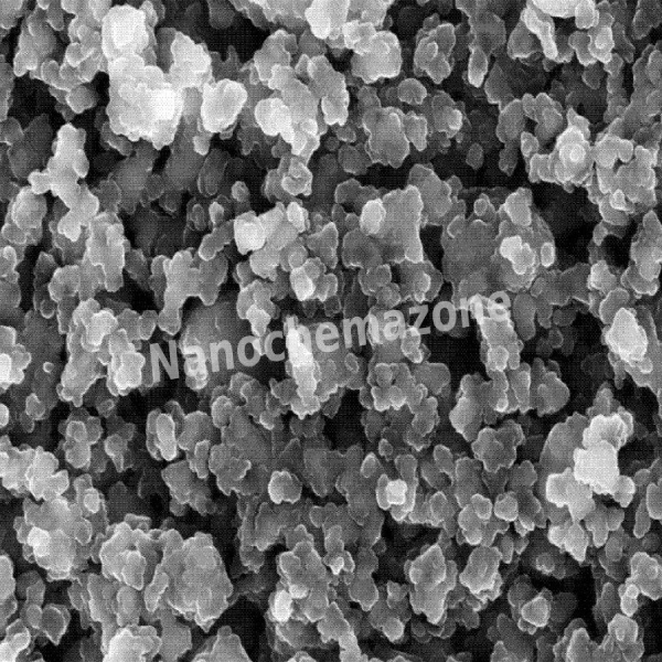
Multi Walled Carbon Nanotubes Ethanol Dispersion
3 wt%, Purity: > 95+ %, OD: 18-28 nm, Length: 8-28 µm
Technical Properties:
| Purity |
> 95+ wt% |
| Color |
black |
| Average Outside Diameter (nm) |
18-28 |
| Average Inside Diameter (nm) |
5.0-10.0 |
| Length (µm) |
8-28 |
| Tap Density (g/cm3) |
0.30 |
| True Density (g/cm3) |
2.4 |
| Specific Surface Area (m2/g) |
120 |
| Ash |
< 1.5 wt% |
| Electrical Conductivity (S/cm) |
> 98 |
| Manufacturing Method |
CVD |
Applications:
MWCNTs have a variety of potential applications in different fields. These applications include medicine, mechanical, electric, chemical, energy and others.
It can be applied in, 1-drug delivery, 2-biosensors, 3-CNT composites, 4-catalysis, 5-nanoprobes, 6-hydrogen storage, 7-lithium batteries, 8-gas-discharge tubes,
9-flat panel display, 10-supercapacitor, 11-transistors, 12-solar cells, 13-photoluminescence, 14-template