Applications of Sputtering Targets;
For film deposition, sputtering targets are employed. Using a "target" source to erode material onto a "substrate" like a silicon wafer, sputter targets are a technique for depositing thin layers.
Targets are etched using semiconductor sputtering targets. When etching anisotropy is required to a great degree and selectivity is not an issue, sputter etching is the method of choice.
By etching away the target material, sputter targets are also utilized for investigation.
In one instance, the target sample is sputtered at a steady pace in secondary ion spectroscopy (SIMS). Using mass spectrometry, the concentration and identity of the spewed atoms are determined when the target is sputtered.
The target material's composition may be ascertained and even very low concentrations of contaminants can be found with the aid of the sputtering target.
There is also an application area for sputtering targets in space. One type of space weathering that alters the chemical and physical characteristics of airless worlds like the Moon and asteroids is sputtering.
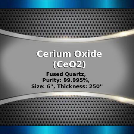
The most prevalent rare-earth element in the crust of the earth is cerium, a metal that belongs to the lanthanide series. Cerium oxide's high refractive index and dielectric constant make it suitable for a wide range of optical and electrical applications. Additionally, cerium oxide can be used for corrosion protection coatings rather than coatings based on chromate.