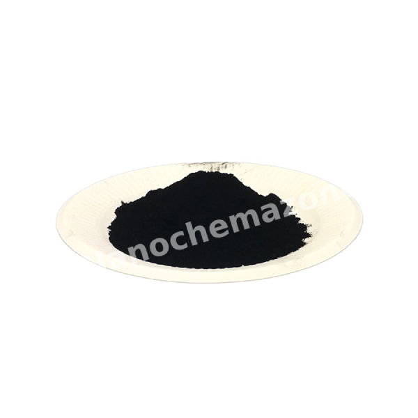
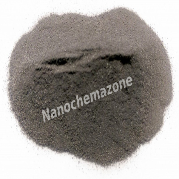
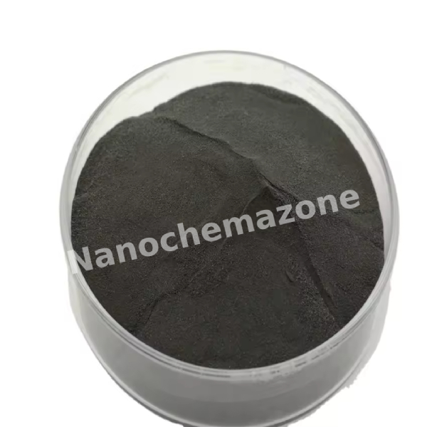
Vanadium Nitrade (VN) Nanopowder, APS: 40nm, Purity: 99.9%
Performance characteristics
Nano vanadium nitride powder is prepared by high frequency plasma gas phase synthesis method, with high purity, no free carbon black dot impurities, no ammonium chloride impurities, uniform particle size distribution, large mass production, and can be applied to cemented carbide in large quantities Its surface activity can be well dispersed in the alloy material and play the role of alloy dispersion strengthening. Vanadium nitride, also known as vanadium-nitrogen alloy, is a new type of alloy additive that can replace ferro-vanadium in the production of microalloyed steel. The addition of vanadium nitride to steel can improve the comprehensive mechanical properties of steel such as strength, toughness, ductility and thermal fatigue resistance, and make the steel have good weldability. When the same strength is reached, adding nano-vanadium nitride can save 30-40% of vanadium addition, thereby reducing costs.
Applications
- Vanadium-nitrogen alloy can be used in structural steel, tool steel, pipe steel, steel bar and cast iron. Vanadium-nitrogen alloy used in high-strength low-alloy steel can simultaneously carry out effective vanadium and nitrogen microalloying, promote the precipitation of carbon, vanadium, and nitrogen compounds in the steel, and more effectively play the role of settlement strengthening and grain refinement;
- Nano-vanadium nitride (VN) has very high thermal, chemical stability and strong mechanical properties, and is widely used in cutting tools, abrasive tools and structural materials; it is also a good catalyst with high catalytic activity and high selectivity , Good stability and anti-poisoning performance. Fine-grained VN can effectively increase the catalytic activity and improve the toughness of structural materials.
Packaging and storage
This product is packaged in an inert gas plastic bag, sealed and stored in a dry, cool environment. It should not be exposed to the air to prevent oxidation and agglomeration due to moisture, which will affect the dispersion performance and use effect; the number of packages can be provided according to customer requirements and packed.