5 grams/29 €
25 grams/58 €
100 grams/85 €
500 grams/384 €
1000 grams/694€
Please contact us for quotes on larger quantities !!!
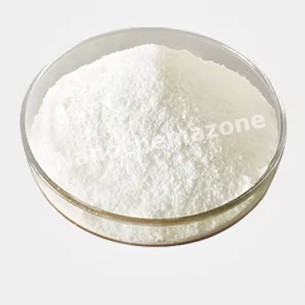
Silicon Nitride (Si3N4) Nanopowder/Nanoparticles
Amorphous, Purity: 99.5%, Size: 20-35 nm
Storage Condition:
Silicon nitride nanoparticles should be sealed in vacuum and stored in cool and dry room. It should not be exposure to air and avoid stress.
Applications:
Silicon nitride nanoparticles is a super hard material. It is used in manufacturing structure devices such as chemical industry, aviation, metallurgy,
machinery, aerospace, and energy industry. It is used in high temperature, waer resistant, and corrosion resistant structural component such as
sleeves, valves, sliding bearings, ball and roller bearings. It is also used in surface treatment of metals and other materials such as cutting tools,
turbine blades and rotors, molds, and cylinder wall coatings. Silicon nitride nanoparticles is also used in composite materials such as metals,
rubbers, plastics, ceramics, coatings, and polymers.