5 grams/59 €
25 grams/98 €
100 grams/196 €
500 grams/485 €
1000 grams/765 €
Please contact us for quotes on larger quantities !!!
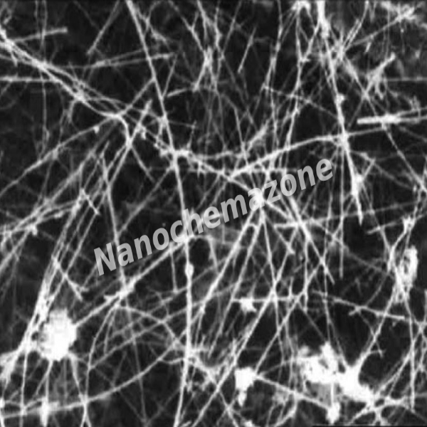
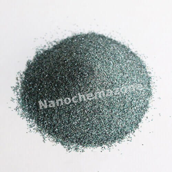
Silicon Carbide (SiC) Nanopowder/Nanoparticles
Beta, Purity: 99.5+%, Size: < 70 nm
Storage Condition:
Silicon Carbide nanoparticles should be sealed in vacuum and stored in cool and dry room. It should not be exposure to air and avoid stress.
Applications:
Silicon carbide nanopowder can be used as a hard and high grade refractory material. It can be used in ceramics such as ceramic besrings,
textile ceramics, high frequency ceramics, and ceramic engine parts. It also can be used in hard discs, polishing abrasives, grinding wheels,
and as a support for multichip modules. Silicon carbide nanopowder has also high thermal conductivity. It can be used in high temperature
sealing valves, high temperature spray nozzles, and high temperature fluid transport parts. It aslo can be used in composites to increase
strength and heat resistance.