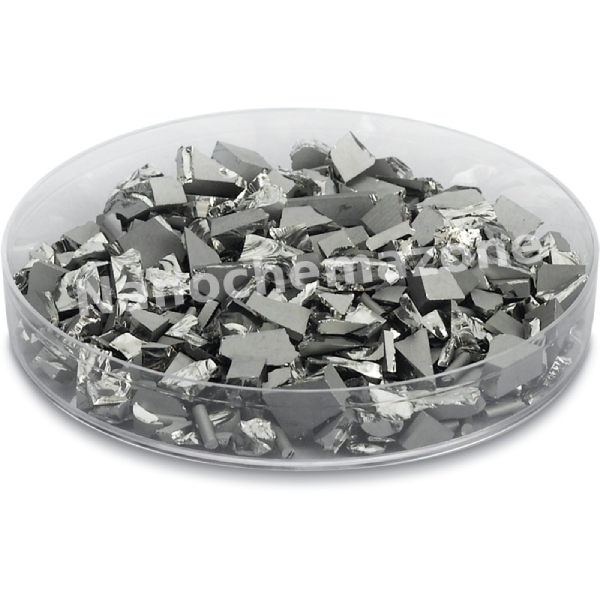
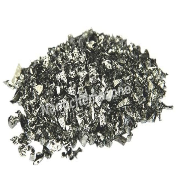
Germanium (Ge) Sputtering Targets, indium, Purity: 99.999%, Size: 2”, Thickness: 0.125”

$436.00

Applications of Sputtering Targets;

Film deposition is accomplished using sputtering targets. A technique for sputtering thin films is called "deposition made by sputter targets," which entails eroding material from a "target" source onto a "substrate" like a silicon wafer. Etching of the target is done using semiconductor sputtering targets. When selectivity is not an issue and a high degree of etching anisotropy is required, sputter etching is the method of choice. By removing the target material through etching, sputter targets are also utilized for investigation. In secondary ion spectroscopy (SIMS), one example is when the target material is sputtered at a steady pace. Mass spectrometry is used to quantify the concentration and identity of spewed atoms as the target is sputtered.

The target material's composition may be ascertained and even very low concentrations of contaminants can be found with the aid of the sputtering target.

There is also an application area for sputtering targets in space. One type of space weathering that alters the chemical and physical characteristics of airless worlds like the Moon and asteroids is sputtering.

Germanium (Ge) Sputtering Targets, Purity: 99.999%, Size: 3”, Thickness: 0.250”

$436.00

Applications of Sputtering Targets;

Film deposition is accomplished using sputtering targets. A technique for sputtering thin films is called "deposition made by sputter targets," which entails eroding material from a "target" source onto a "substrate" like a silicon wafer. Etching of the target is done using semiconductor sputtering targets. When selectivity is not an issue and a high degree of etching anisotropy is required, sputter etching is the method of choice. By removing the target material through etching, sputter targets are also utilized for investigation. In secondary ion spectroscopy (SIMS), one example is when the target material is sputtered at a steady pace. Mass spectrometry is used to quantify the concentration and identity of spewed atoms as the target is sputtered.

The target material's composition may be ascertained and even very low concentrations of contaminants can be found with the aid of the sputtering target.

There is also an application area for sputtering targets in space. One type of space weathering that alters the chemical and physical characteristics of airless worlds like the Moon and asteroids is sputtering.

Germanium (Ge) Sputtering Targets, Purity: 99.999%, Size: 4”, Thickness: 0.250”

$436.00

Applications of Sputtering Targets;

Film deposition is accomplished using sputtering targets. A technique for sputtering thin films is called "deposition made by sputter targets," which entails eroding material from a "target" source onto a "substrate" like a silicon wafer. Etching of the target is done using semiconductor sputtering targets. When selectivity is not an issue and a high degree of etching anisotropy is required, sputter etching is the method of choice. By removing the target material through etching, sputter targets are also utilized for investigation. In secondary ion spectroscopy (SIMS), one example is when the target material is sputtered at a steady pace. Mass spectrometry is used to quantify the concentration and identity of spewed atoms as the target is sputtered.

The target material's composition may be ascertained and even very low concentrations of contaminants can be found with the aid of the sputtering target.

There is also an application area for sputtering targets in space. One type of space weathering that alters the chemical and physical characteristics of airless worlds like the Moon and asteroids is sputtering.

Tungsten Disulfide (WS2) Sputtering Targets, Purity: 99.9%, Size: 8”, Thickness: 0.250”

$436.00

Applications of Sputtering Targets;

Film deposition is accomplished using sputtering targets. A technique for sputtering thin films is called "deposition made by sputter targets," which entails eroding material from a "target" source onto a "substrate" like a silicon wafer. Etching of the target is done using semiconductor sputtering targets. When selectivity is not an issue and a high degree of etching anisotropy is required, sputter etching is the method of choice. By removing the target material through etching, sputter targets are also utilized for investigation. In secondary ion spectroscopy (SIMS), one example is when the target material is sputtered at a steady pace. Mass spectrometry is used to quantify the concentration and identity of spewed atoms as the target is sputtered.

The target material's composition may be ascertained and even very low concentrations of contaminants can be found with the aid of the sputtering target.

There is also an application area for sputtering targets in space. One type of space weathering that alters the chemical and physical characteristics of airless worlds like the Moon and asteroids is sputtering.

Chromium Oxide (Cr2O3) Sputtering Targets, Purity: 99.8%-99.9%, Size: 2”, Thickness: 0.125”

$436.00

Product 

Chromium Oxide (Cr2O3) Sputtering Targets, Purity: 99.8%-99.9%, Size: 2'', Thickness: 0.125''

CAS No.

1308-38-9

Appearance

Powder

Purity

≥99%,  ≥99.9%,  ≥95%

(Other purities are also available)

APS

 N/A (Size Can be customized), Ask for other available size ranges.

Ingredient

N/A

Molecular Weight

 151.99 g/mol

Melting Point

2,435 °C

Boiling Point

 ~3,000 °C (approximate; may decompose before boiling)

Density

5.21 g/cm³

Product Codes

NCZ-2304K

Silver (Ag) Sputtering Targets, Purity: 99.99%, Size: 3”, Thickness: 0.125”

$437.00

Product 

Silver (Ag) Sputtering Targets, Purity: 99.99%, Size: 3'', Thickness: 0.125''

CAS No.

 7440-22-4

Appearance

Powder

Purity

≥99%,  ≥99.9%,  ≥95%

(Other purities are also available)

APS

N/A  (Size Can be customized), Ask for other available size ranges.

Ingredient

N/A

Molecular Weight

107.87 g/mol

Melting Point

 961.78 °C

Boiling Point

 2162 °C

Density

 10.49 g/cm³

Product Codes

NCZ-1690K

Silver (Ag) Sputtering Targets, Purity: 99.99%, Size: 2”, Thickness: 0.250”

$437.00

Product 

Silver (Ag) Sputtering Targets, Purity: 99.99%, Size: 2'', Thickness: 0.250''

CAS No.

 7440-22-4

Appearance

Powder

Purity

≥99%,  ≥99.9%,  ≥95%

(Other purities are also available)

APS

N/A  (Size Can be customized), Ask for other available size ranges.

Ingredient

N/A

Molecular Weight

107.87 g/mol

Melting Point

 961.78 °C

Boiling Point

 2162 °C

Density

 10.49 g/cm³

Product Codes

NCZ-1691K

Gold Nanostars, Size: 40-45 nm

Price range: $438.00 through $5,982.00
Select options This product has multiple variants. The options may be chosen on the product page
Gold Nanostars, 40-45 nm Gold Nanostars are gold nanoparticles having multiple sharp and pointed branches in a genuine star-shaped. This unique

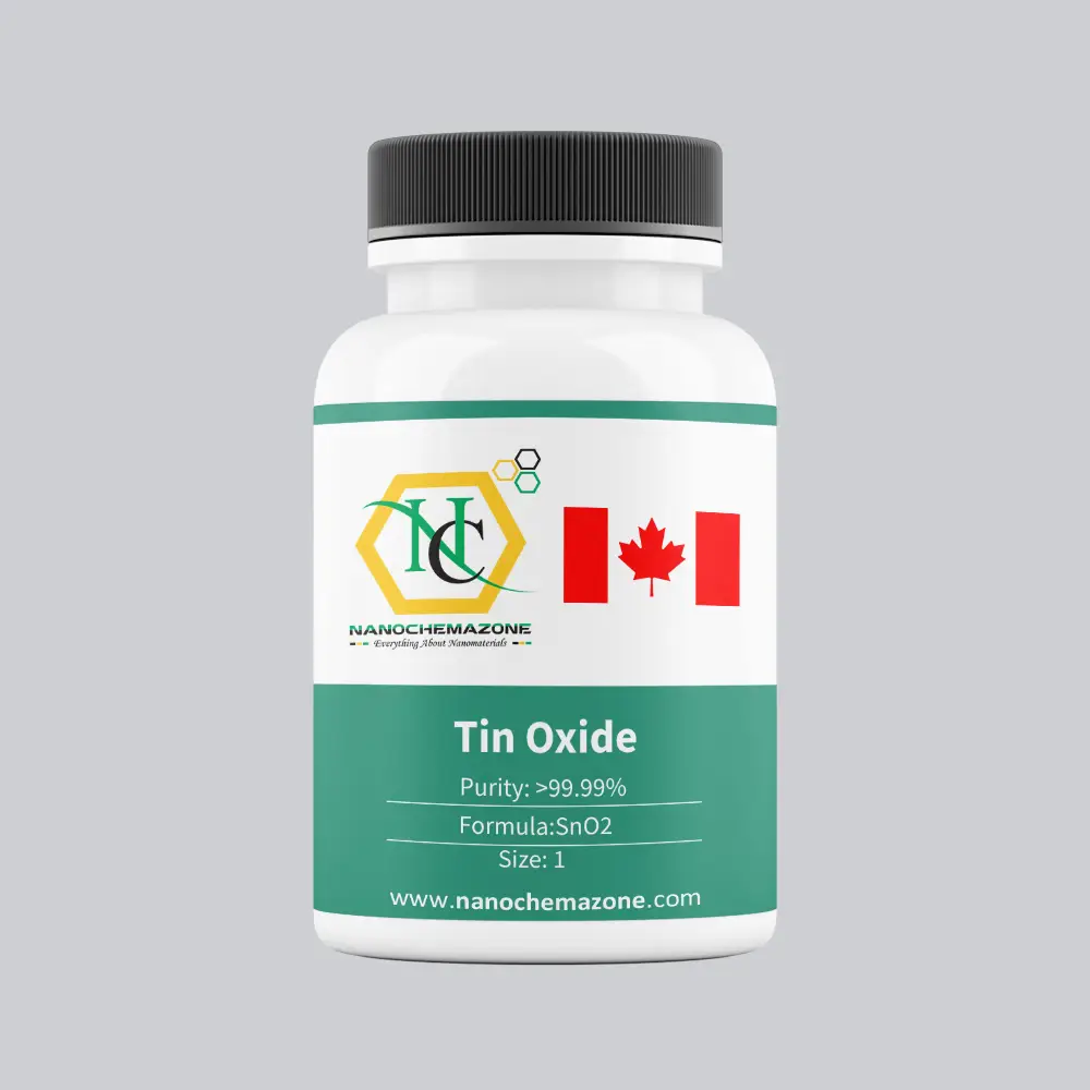
Tin Oxide (SnO2) Sputtering Targets, Purity: 99.99%, Size: 1”, Thickness: 0.250”

$438.00

Applications of Sputtering Targets;

Film deposition is accomplished using sputtering targets. A technique for sputtering thin films is called "deposition made by sputter targets," which entails eroding material from a "target" source onto a "substrate" like a silicon wafer. Etching of the target is done using semiconductor sputtering targets. When selectivity is not an issue and a high degree of etching anisotropy is required, sputter etching is the method of choice. By removing the target material through etching, sputter targets are also utilized for investigation. In secondary ion spectroscopy (SIMS), one example is when the target material is sputtered at a steady pace. Mass spectrometry is used to quantify the concentration and identity of spewed atoms as the target is sputtered.

The target material's composition may be ascertained and even very low concentrations of contaminants can be found with the aid of the sputtering target.

There is also an application area for sputtering targets in space. One type of space weathering that alters the chemical and physical characteristics of airless worlds like the Moon and asteroids is sputtering.

Gallium Antimonide (GaSb) Wafers, Size: 2”, Thickness: 500± 25 μm, Orientation: 111, Testing Grade

Price range: $439.00 through $2,031.00
Select options This product has multiple variants. The options may be chosen on the product page
  1 piece/396  5 pieces/1830                          Please contact us for quotes on larger quantities !!!

Gallium Antimonide (GaSb) Wafers

Size: 2”, Thickness: 500± 25 μm, Orientation: 111

Technical Properties:

Quality  Testing Grade
Size (inch)  2”
Thickness (μm)  500± 25
Polished  Single Side
Dopant  Tellurium ( N type )
Orientation  111
Mobility  2000-3500
EPD  ≤2000
Growth method  VGF
OF Length  16±2
IF Length   8±1

Fields of Application for Gallium Antimonide (GaSb)

The intermetallic compound of gallium antimonide (GaSb) was first prepared in 1926 by Victor Goldschmidt. Gallium antimonide (GaSb) is a semiconductor made of gallium and antimony of the group III-V compounds. Gallium antimonide (GaSb) is supplied in polished wafer form. Gallium antimonide (GaSb) wafers are produced from polycrystalline ingots with using Czochralski method to obtain a single crystal with perfect purity. Supplied in polished wafer form, gallium antimonide has a very high accuracy of orientation. Thickness and orientation of these wafers can be modified with additives. Czochralski method is used to provide the growh of pure gallium and antimonide elements. The natural low-defect structure of GaSb makes it a perfect material for epitaxial growth. They are supplied in polished 1 side or 2 sides and cut forms.
  • Gallium antimonide (GaSb) is used for infrared detectors.
  • Gallium antimonide (GaSb) is used for infrared LEDs.
  • Gallium antimonide (GaSb) is used for transistors.
  • Gallium antimonide (GaSb) is used for lasers.
  • Gallium antimonide (GaSb) is used for thermophotovoltaic systems.

Gallium Antimonide (GaSb) Wafers, Size: 2”, Thickness: 500± 25 μm, Orientation: 100, Testing Grade

Price range: $439.00 through $2,031.00
Select options This product has multiple variants. The options may be chosen on the product page
1 piece/396  5 pieces/1830                            Please contact us for quotes on larger quantities !!!

Gallium Antimonide (GaSb) Wafers

Size: 2”, Thickness: 500± 25 μm, Orientation: 100

Technical Properties:

Quality  Testing Grade
Size (inch)  2”
Thickness (μm)  500± 25
Polished  Single Side
Dopant  Tellurium ( N type )
Orientation  100
Mobility  2000-3500
EPD  ≤2000
Growth method  VGF
OF Length  16±2
IF Length   8±1

Fields of Application for Gallium Antimonide (GaSb)

The intermetallic compound of gallium antimonide (GaSb) was first prepared in 1926 by Victor Goldschmidt. Gallium antimonide (GaSb) is a semiconductor made of gallium and antimony of the group III-V compounds. Gallium antimonide (GaSb) is supplied in polished wafer form. Gallium antimonide (GaSb) wafers are produced from polycrystalline ingots with using Czochralski method to obtain a single crystal with perfect purity. Supplied in polished wafer form, gallium antimonide has a very high accuracy of orientation. Thickness and orientation of these wafers can be modified with additives. Czochralski method is used to provide the growh of pure gallium and antimonide elements. The natural low-defect structure of GaSb makes it a perfect material for epitaxial growth. They are supplied in polished 1 side or 2 sides and cut forms.
  • Gallium antimonide (GaSb) is used for infrared detectors.
  • Gallium antimonide (GaSb) is used for infrared LEDs.
  • Gallium antimonide (GaSb) is used for transistors.
  • Gallium antimonide (GaSb) is used for lasers.

Indium Tin Oxide/ITO (In203:Sn02) Sputtering Targets, Purity: 99.99%, Size: 1”, Thickness: 0.125”

$439.00

Applications of Sputtering Targets;

Film deposition is accomplished using sputtering targets. A technique for sputtering thin films is called "deposition made by sputter targets," which entails eroding material from a "target" source onto a "substrate" like a silicon wafer. Etching of the target is done using semiconductor sputtering targets. When selectivity is not an issue and a high degree of etching anisotropy is required, sputter etching is the method of choice. By removing the target material through etching, sputter targets are also utilized for investigation. In secondary ion spectroscopy (SIMS), one example is when the target material is sputtered at a steady pace. Mass spectrometry is used to quantify the concentration and identity of spewed atoms as the target is sputtered.

The target material's composition may be ascertained and even very low concentrations of contaminants can be found with the aid of the sputtering target.

There is also an application area for sputtering targets in space. One type of space weathering that alters the chemical and physical characteristics of airless worlds like the Moon and asteroids is sputtering.

Indium Tin Oxide/ITO (In203:Sn02) Sputtering Targets, Purity: 99.99%, Size: 3”, Thickness: 0.125”

$439.00

Applications of Sputtering Targets;

Film deposition is accomplished using sputtering targets. A technique for sputtering thin films is called "deposition made by sputter targets," which entails eroding material from a "target" source onto a "substrate" like a silicon wafer. Etching of the target is done using semiconductor sputtering targets. When selectivity is not an issue and a high degree of etching anisotropy is required, sputter etching is the method of choice. By removing the target material through etching, sputter targets are also utilized for investigation. In secondary ion spectroscopy (SIMS), one example is when the target material is sputtered at a steady pace. Mass spectrometry is used to quantify the concentration and identity of spewed atoms as the target is sputtered.

The target material's composition may be ascertained and even very low concentrations of contaminants can be found with the aid of the sputtering target.

There is also an application area for sputtering targets in space. One type of space weathering that alters the chemical and physical characteristics of airless worlds like the Moon and asteroids is sputtering.

Niobium Oxide (Nb2O5) Sputtering Targets, Purity: 99.5%, Size: 3”, Thickness: 0.250”

$439.00

Product 

Niobium Oxide (Nb2O5) Sputtering Targets, Purity: 99.5%, Size: 3'', Thickness: 0.250''

CAS No.

1313-96-8

Appearance

Powder

Purity

≥99%,  ≥99.9%,  ≥95%

(Other purities are also available)

APS

N/A (Size Can be customized), Ask for other available size ranges.

Ingredient

N/A

Molecular Weight

 265.81 g/mol

Melting Point

~1512 °C

Boiling Point

N/A

Density

 4.6 – 4.9 g/cm³

Product Codes

NCZ-1807K

Nickel Vanadium (NiV) Sputtering Targets, Purity: 99.95%, Size: 4”, Thickness: 0.250”

$439.00

Product 

Nickel Vanadium (NiV) Sputtering Targets, Purity: 99.95%, Size: 4'', Thickness: 0.250''

CAS No.

11137-91-4

Appearance

Powder

Purity

≥99%,  ≥99.9%,  ≥95%

(Other purities are also available)

APS

N/A (Size Can be customized), Ask for other available size ranges.

Ingredient

N/A

Molecular Weight

~57.9 g/mol

Melting Point

~1,350–1,450 °C

Boiling Point

N/A

Density

 ~8.5 g/cm³

Product Codes

NCZ-1823K

5N (99.999%) Germanium (Ge) Pieces Evaporation Materials

Price range: $440.00 through $4,004.00
Select options This product has multiple variants. The options may be chosen on the product page
Product 5N (99.999%) Germanium (Ge) Pieces Evaporation Materials
CAS No. N/A
Appearance Grayish White, Semi-Metallic
Purity ≥99%,  ≥99.9%,  ≥95%(Other purities are also available)
APS N/A.
Ingredient Ge
Molecular Weight N/A
Melting Point 937 °C
Boiling Point N/A
Density N/A
Product Codes NCZ-115E

Hafnium (Hf) Sputtering Target

Price range: $440.00 through $2,850.00
Select options This product has multiple variants. The options may be chosen on the product page

Product 

Hafnium (Hf) Sputtering Target

CAS No.

7440-58-6

Appearance

Powder

Purity

≥99%,  ≥99.9%,  ≥95%

(Other purities are also available)

APS

 NA (Size Can be customized), Ask for other available size ranges.

Ingredient

N/A

Molecular Weight

 178.49 g/mol

Melting Point

2,233 °C

Boiling Point

4,603 °C

Density

13.31 g/cm³

Product Codes

NCZ-1291K

Cadmium Sulfide (CdS) Sputtering Target

Price range: $440.00 through $1,010.00
Select options This product has multiple variants. The options may be chosen on the product page

Product 

Cadmium Sulfide (CdS) Sputtering Target

CAS No.

1306-23-6

Appearance

Powder

Purity

≥99%,  ≥99.9%,  ≥95%

(Other purities are also available)

APS

 NA (Size Can be customized), Ask for other available size ranges.

Ingredient

N/A

Molecular Weight

144.48 g/mol

Melting Point

~1,750 °C

Boiling Point

~980 °C

Density

~4.82 g/cm³

Product Codes

NCZ-1341K

5N (99.999%) Germanium (Ge) Pieces Evaporation Materials

Price range: $440.00 through $4,004.00
Select options This product has multiple variants. The options may be chosen on the product page
Product 5N (99.999%) Germanium (Ge) Pieces Evaporation Materials
CAS No. 7440-56-4
Appearance Grayish White, Semi-Metallic
Purity ≥99%,  ≥99.9%,  ≥95%(Other purities are also available)
APS N/A
Ingredient Ge
Molecular Weight 72.63 g/mol
Melting Point 937 °C
Boiling Point N/A
Density 5.32 g/cm³
Product Codes NCZ-199I

Silicon (Si) Sputtering Targets, N-type, Purity: 99.999%, Size: 3”, Thickness: 0.125”

$440.00

Product 

Silicon (Si) Sputtering Targets, N-type, Purity: 99.999%, Size: 3'', Thickness: 0.125''

CAS No.

7440-21-3

Appearance

Powder

Purity

≥99%,  ≥99.9%,  ≥95%

(Other purities are also available)

APS

N/A  (Size Can be customized), Ask for other available size ranges.

Ingredient

N/A

Molecular Weight

28.0855 g/mol

Melting Point

 1,414 °C

Boiling Point

3,265 °C

Density

 2.33 g/cm³

Product Codes

NCZ-1763K

Magnesium Fluoride (MgF2) Sputtering Targets, Purity: 99.9%, Size: 1”, Thickness: 0.250”

$440.00

Product 

Magnesium Fluoride (MgF2) Sputtering Targets, Purity: 99.9%, Size: 1'', Thickness: 0.250''

CAS No.

7783-40-6

Appearance

Powder

Purity

≥99%,  ≥99.9%,  ≥95%

(Other purities are also available)

APS

 N/A (Size Can be customized), Ask for other available size ranges.

Ingredient

N/A

Molecular Weight

 62.30 g/mol

Melting Point

~1263 °C

Boiling Point

~2260 °C

Density

 3.18 g/cm³

Product Codes

NCZ-1985K

Vanadium Oxide (V2O5) Sputtering Targets, Purity: 99.9%, Size: 1”, Thickness: 0.125”

$441.00

Product 

Vanadium Oxide (V2O5) Sputtering Targets, Purity: 99.9%, Size: 1'', Thickness: 0.125''

CAS No.

1314‑62‑1

Appearance

Powder

Purity

≥99%,  ≥99.9%,  ≥95%

(Other purities are also available)

APS

N/A  (Size Can be customized), Ask for other available size ranges.

Ingredient

N/A

Molecular Weight

181.88 g/mol

Melting Point

690 °C

Boiling Point

~1750 °C

Density

~3.35 g/cm³

Product Codes

NCZ-1542K

Tungsten Titanium (TiW) Sputtering Targets, Purity: 99.99%, Size: 6”, Thickness: 0.125”

$441.00

Product 

Tungsten Titanium (TiW) Sputtering Targets, Purity: 99.99%, Size: 6'', Thickness: 0.125''

CAS No.

58397-70-9

Appearance

Powder

Purity

≥99%,  ≥99.9%,  ≥95%

(Other purities are also available)

APS

N/A  (Size Can be customized), Ask for other available size ranges.

Ingredient

N/A

Molecular Weight

~231.71 g/mol

Melting Point

~2,700–3,200 °C

Boiling Point

~4,500–5,000 °C

Density

~14.5–17.0 g/cm³

Product Codes

NCZ-1554K

Silicon (Si) Sputtering Targets, P-type, Purity: 99.999%, Size: 8”, Thickness: 0.125”

$441.00

Product 

Silicon (Si) Sputtering Targets, P-type, Purity: 99.999%, Size: 8'', Thickness: 0.125''

CAS No.

7440-21-3

Appearance

Powder

Purity

≥99%,  ≥99.9%,  ≥95%

(Other purities are also available)

APS

N/A  (Size Can be customized), Ask for other available size ranges.

Ingredient

N/A

Molecular Weight

28.0855 g/mol

Melting Point

 1,414 °C

Boiling Point

3,265 °C

Density

 2.33 g/cm³

Product Codes

NCZ-1743K

Nickel Vanadium (NiV) Sputtering Targets, Purity: 99.95%, Size: 8”, Thickness: 0.250”

$442.00

Applications of Sputtering Targets;

Film deposition is accomplished using sputtering targets. A technique for sputtering thin films is called "deposition made by sputter targets," which entails eroding material from a "target" source onto a "substrate" like a silicon wafer. Etching of the target is done using semiconductor sputtering targets. When selectivity is not an issue and a high degree of etching anisotropy is required, sputter etching is the method of choice. By removing the target material through etching, sputter targets are also utilized for investigation. In secondary ion spectroscopy (SIMS), one example is when the target material is sputtered at a steady pace. Mass spectrometry is used to quantify the concentration and identity of spewed atoms as the target is sputtered.

The target material's composition may be ascertained and even very low concentrations of contaminants can be found with the aid of the sputtering target.

There is also an application area for sputtering targets in space. One type of space weathering that alters the chemical and physical characteristics of airless worlds like the Moon and asteroids is sputtering.

Niobium Oxide (Nb2O5) Sputtering Targets, Purity: 99.5%, Size: 4”, Thickness: 0.125”

$442.00

Applications of Sputtering Targets;

Film deposition is accomplished using sputtering targets. A technique for sputtering thin films is called "deposition made by sputter targets," which entails eroding material from a "target" source onto a "substrate" like a silicon wafer. Etching of the target is done using semiconductor sputtering targets. When selectivity is not an issue and a high degree of etching anisotropy is required, sputter etching is the method of choice. By removing the target material through etching, sputter targets are also utilized for investigation. In secondary ion spectroscopy (SIMS), one example is when the target material is sputtered at a steady pace. Mass spectrometry is used to quantify the concentration and identity of spewed atoms as the target is sputtered.

The target material's composition may be ascertained and even very low concentrations of contaminants can be found with the aid of the sputtering target.

There is also an application area for sputtering targets in space. One type of space weathering that alters the chemical and physical characteristics of airless worlds like the Moon and asteroids is sputtering.

Calcium Manganate (CaMnO3) Sputtering Targets, Purity: 99.9%, Size: 3”, Thickness: 0.250”

$442.00

Product 

Calcium Manganate (CaMnO3) Sputtering Targets, Purity: 99.9%, Size: 3'', Thickness: 0.250''

CAS No.

12058-85-6

Appearance

Powder

Purity

≥99%,  ≥99.9%,  ≥95%

(Other purities are also available)

APS

 N/A (Size Can be customized), Ask for other available size ranges.

Ingredient

N/A

Molecular Weight

157.87 g/mol

Melting Point

 Approx. 1400 °C (decomposes)

Boiling Point

N/A

Density

 ~4.7 g/cm³

Product Codes

NCZ-2358K

Aluminum Oxide (Al2O3) Sputtering Targets, Purity: 99.99%, Size: 2”, Thickness: 0.250”

$443.00

Product 

Aluminum Oxide (Al2O3) Sputtering Targets, Purity: 99.99%, Size: 2'', Thickness: 0.250''

CAS No.

 1344-28-1

Appearance

Powder

Purity

≥99%,  ≥99.9%,  ≥95%

(Other purities are also available)

APS

N/A (Size Can be customized), Ask for other available size ranges.

Ingredient

N/A

Molecular Weight

101.96 g/mol

Melting Point

~2,072 °C

Boiling Point

~2,977 °C

Density

~3.97–3.98 g/cm³

Product Codes

NCZ-2543K

Sodium Hyaluronate(powder, Injection grade , ≥95%) (338644)

$443.00
Select options This product has multiple variants. The options may be chosen on the product page
Sodium Hyaluronate(powder, Injection grade , ≥95%) (338644)

  Specifications
Test Items Standard
Appearance White powder
Hyaluronic Acid 95.0%--105.0%
Molecular weight (0.5-1.0)x106
pH 5.0-7.5
Chlorides ≤0.5
600nm.The optical absorption 1-300 0.01
260 nm optical absorption 1-300 0.5
Loss on drying ≤10%
Protein ≤0.05%
Iron ≤10ppm
Bacterial counts ≤10cfu/g
Heavy metals 3ppm
cadmium 1ppm
mercury 0.1 ppm.
Endotoxin ≤0.05eu/mg
Sterile Test Complies
    Product Codes- NCZ-2705K

Silicon Carbide Wafer (SiC-4H) – 4H, Size: 3”, Thickness: 350 μm, Production Grade, 4H Area: 100%

Price range: $444.00 through $2,028.00
Select options This product has multiple variants. The options may be chosen on the product page
Silicon Carbide Wafer (SiC-4H)-4H Size: 3”, Thickness: 350 μm, 4H Area: 100% Technical Properties: Quality  Production Grade Size (inch)  3” Thickness (μm)

High Purity Atomized Spherical Magnesium (Mg) Powder NGW20

Price range: $445.00 through $2,694.00
Select options This product has multiple variants. The options may be chosen on the product page
500 grams/395 € 1 kg/565 € 5 kg/2390 €   
Please contact us for quotes on larger quantities !!!

High Purity Atomized Spherical Magnesium (Mg) Powder NGW20

High purity atomized spherical magnesium powder is manufacturing by the centrifugal atomization technology that is melting minimum 99.8% purity magnesium and spraying the molten metal under the protection of an inert atmosphere. High purity atomized spherical magnesium powder is known with the outstanding features of high apparent density, high content of active magnesium, high fluidity, high stability, small particle size and small specific surface, and so on.

Technical Properties:

Particle Shape

Spherical Particle

Spherical Rate (%)

≥95

Apparent Density (g·cm-3 )

0.9 (min)

Bulk Density (g·cm-3 )

0.70 (min)

Liquidity (s·(50g)-1 )

78.6

Moisture Absorption (%)

0.01

Active Mg Content (%)

99.0 (min)

D50 (µm)

20±4

Impurity Content (%)

Moisture Content (%max)

0.08

HCl Undissolved Substance (%max)

0.047

Oil Content (%max)

0.00

Fe (%max)

0.045

Mn (%max)

0.008

Zn (%max)

0.008

Cl (%max)

0.004


Applications:

High purity atomized spherical magnesium powder is widely used in the fields like aviation, national defense, composite materials, powder metallurgy, petrochemical catalyst, electronic coating, medicine, foods and new type functional materials and so on.

Silicon (Si) Sputtering Targets, N-type, Purity: 99.999%, Size: 8”, Thickness: 0.125”

$445.00

Applications of Sputtering Targets;

Film deposition is accomplished using sputtering targets. A technique for sputtering thin films is called "deposition made by sputter targets," which entails eroding material from a "target" source onto a "substrate" like a silicon wafer. Etching of the target is done using semiconductor sputtering targets. When selectivity is not an issue and a high degree of etching anisotropy is required, sputter etching is the method of choice. By removing the target material through etching, sputter targets are also utilized for investigation. In secondary ion spectroscopy (SIMS), one example is when the target material is sputtered at a steady pace. Mass spectrometry is used to quantify the concentration and identity of spewed atoms as the target is sputtered.

The target material's composition may be ascertained and even very low concentrations of contaminants can be found with the aid of the sputtering target.

There is also an application area for sputtering targets in space. One type of space weathering that alters the chemical and physical characteristics of airless worlds like the Moon and asteroids is sputtering.

Vanadium Oxide (V2O5) Sputtering Targets, Purity: 99.9%, Size: 2”, Thickness: 0.250”

$445.00

Applications of Sputtering Targets;

Film deposition is accomplished using sputtering targets. A technique for sputtering thin films is called "deposition made by sputter targets," which entails eroding material from a "target" source onto a "substrate" like a silicon wafer. Etching of the target is done using semiconductor sputtering targets. When selectivity is not an issue and a high degree of etching anisotropy is required, sputter etching is the method of choice. By removing the target material through etching, sputter targets are also utilized for investigation. In secondary ion spectroscopy (SIMS), one example is when the target material is sputtered at a steady pace. Mass spectrometry is used to quantify the concentration and identity of spewed atoms as the target is sputtered.

The target material's composition may be ascertained and even very low concentrations of contaminants can be found with the aid of the sputtering target.

There is also an application area for sputtering targets in space. One type of space weathering that alters the chemical and physical characteristics of airless worlds like the Moon and asteroids is sputtering.

Nickel (Ni) Sputtering Targets, Purity: 99.99%, Size: 8”, Thickness: 0.125”

$445.00

Product 

Nickel (Ni) Sputtering Targets, Purity: 99.99%, Size: 8'', Thickness: 0.125''

CAS No.

7440-02-0

Appearance

Powder

Purity

≥99%,  ≥99.9%,  ≥95%

(Other purities are also available)

APS

 N/A (Size Can be customized), Ask for other available size ranges.

Ingredient

N/A

Molecular Weight

 58.69 g/mol

Melting Point

 1,455 °C

Boiling Point

 2,732 °C

Density

 8.90 g/cm³

Product Codes

NCZ-1866K

Mesophase pitch(Petroleum, Carbon foam grade) (277575)

$445.00
Select options This product has multiple variants. The options may be chosen on the product page
Mesophase pitch(Petroleum, Carbon foam grade) (277575)
 
Softening point Content of mesophase Coking value Ash
310-375°C >95% >88% 0.01%
    Product Codes- NCZ-2673K

Vanadium Oxide (V2O5) Sputtering Target

Price range: $446.00 through $965.00
Select options This product has multiple variants. The options may be chosen on the product page

Product 

Vanadium Oxide (V2O5) Sputtering Target

CAS No.

 1314-62-1

Appearance

Powder

Purity

≥99%,  ≥99.9%,  ≥95%

(Other purities are also available)

APS

 NA (Size Can be customized), Ask for other available size ranges.

Ingredient

N/A

Molecular Weight

181.88 g/mol

Melting Point

~690 °C

Boiling Point

~1,750 °C

Density

~3.36 g/cm³

Product Codes

NCZ-1329K

Silicon (Si) Sputtering Targets, undoped, Purity: 99.999%, Size: 3”, Thickness: 0.250”

$446.00

Product 

Silicon (Si) Sputtering Targets, undoped, Purity: 99.999%, Size: 3'', Thickness: 0.250''

CAS No.

7440-21-3

Appearance

Powder

Purity

≥99%,  ≥99.9%,  ≥95%

(Other purities are also available)

APS

N/A  (Size Can be customized), Ask for other available size ranges.

Ingredient

N/A

Molecular Weight

28.0855 g/mol

Melting Point

1,414 °C

Boiling Point

 3,265 °C

Density

 2.33 g/cm³

Product Codes

NCZ-1732K

Indium(III) Oxide (In2O3) Nanopowder, 50nm, ≥99.99% (4N) Purity

Price range: $446.00 through $908.00
Select options This product has multiple variants. The options may be chosen on the product page
Product Indium(III) Oxide (In2O3) Nanopowder, 50nm, ≥99.99% (4N) Purity
CAS No. 1312-43-2
Appearance Yellowish-white or pale tan
Purity ≥99%,  ≥99.9%,  ≥95%(Other purities are also available)
APS 50nm (Size Can be customized),  Ask for other available size range.
Ingredient In2O3
Molecular Weight 277.64 g/mol
Melting Point N/A
Boiling Point N/A
Density 7.18 g/cm³
Product Codes NCZ-430I

Silver-Carbon Nanotube Fibers Composite Wires, Ag-CNT, Diameter: 10-30 µm, Coating Thickness: 1 µm, Electrical conductivity: 1.5×10^7 S/m

Price range: $447.00 through $1,805.00
Select options This product has multiple variants. The options may be chosen on the product page
Silver-Carbon Nanotube Fibers Composite Wires Ag-CNT, Diameter: 10-30 µm, Coating Thickness: 1 µm, Electrical conductivity: 1.5x10⁷ S/m Silver/carbon nanotube composites (Ag/CNT composites) is produced for the demand of superior electrical, thermal and mechanical performances. They are used in many industries and vehicles in order to obtain better conductivity performances. In electronics, they offer better interconnection and thermal management than non-composite materials. This material is highly functional, efficient, and sustainable for the next-generation electrical and electronics systems.

Nickel (Ni) Sputtering Targets, Purity: 99.99%, Size: 8”, Thickness: 0.250”

$447.00

Applications of Sputtering Targets;

Film deposition is accomplished using sputtering targets. A technique for sputtering thin films is called "deposition made by sputter targets," which entails eroding material from a "target" source onto a "substrate" like a silicon wafer.

Etching of the target is done using semiconductor sputtering targets. When selectivity is not an issue and a high degree of etching anisotropy is required, sputter etching is the method of choice. By removing the target material through etching, sputter targets are also utilized for investigation. In secondary ion spectroscopy (SIMS), one example is when the target material is sputtered at a steady pace. Mass spectrometry is used to quantify the concentration and identity of spewed atoms as the target is sputtered.

The target material's composition may be ascertained and even very low concentrations of contaminants can be found with the aid of the sputtering target.

There is also an application area for sputtering targets in space. One type of space weathering that alters the chemical and physical characteristics of airless worlds like the Moon and asteroids is sputtering.

Ytterbium Oxide (Yb2O3) Sputtering Targets, Purity: 99.99%, Size: 1”, Thickness: 0.125”

$447.00

Applications of Sputtering Targets;

Film deposition is accomplished using sputtering targets. A technique for sputtering thin films is called "deposition made by sputter targets," which entails eroding material from a "target" source onto a "substrate" like a silicon wafer. Etching of the target is done using semiconductor sputtering targets. When selectivity is not an issue and a high degree of etching anisotropy is required, sputter etching is the method of choice. By removing the target material through etching, sputter targets are also utilized for investigation. In secondary ion spectroscopy (SIMS), one example is when the target material is sputtered at a steady pace. Mass spectrometry is used to quantify the concentration and identity of spewed atoms as the target is sputtered.

The target material's composition may be ascertained and even very low concentrations of contaminants can be found with the aid of the sputtering target.

There is also an application area for sputtering targets in space. One type of space weathering that alters the chemical and physical characteristics of airless worlds like the Moon and asteroids is sputtering.

Zinc Oxide (ZnO) Sputtering Targets, Purity: 99.999%, Size: 1”, Thickness: 0.125”

$447.00

Product 

Zinc Oxide (ZnO) Sputtering Targets, Purity: 99.999%, Size: 1'', Thickness: 0.125''

CAS No.

1314‑13‑2

Appearance

Powder

Purity

≥99%,  ≥99.9%,  ≥95%

(Other purities are also available)

APS

ZnO (black granules) (Size Can be customized), Ask for other available size ranges.

Ingredient

N/A

Molecular Weight

81.38 g/mol

Melting Point

~1975 °C

Boiling Point

~2360 °C

Density

 ~5.61 g/cm³

Product Codes

NCZ-1456K

Silicon (Si) Sputtering Targets, N-type, Purity: 99.999%, Size: 4”, Thickness: 0.125”

$447.00

Product 

Silicon (Si) Sputtering Targets, N-type, Purity: 99.999%, Size: 4'', Thickness: 0.125''

CAS No.

7440-21-3

Appearance

Powder

Purity

≥99%,  ≥99.9%,  ≥95%

(Other purities are also available)

APS

N/A  (Size Can be customized), Ask for other available size ranges.

Ingredient

N/A

Molecular Weight

28.0855 g/mol

Melting Point

 1,414 °C

Boiling Point

3,265 °C

Density

 2.33 g/cm³

Product Codes

NCZ-1761K

Silicon (Si) Sputtering Targets, N-type, Purity: 99.999%, Size: 3”, Thickness: 0.250”

$447.00

Product 

Silicon (Si) Sputtering Targets, N-type, Purity: 99.999%, Size: 3'', Thickness: 0.250''

CAS No.

7440-21-3

Appearance

Powder

Purity

≥99%,  ≥99.9%,  ≥95%

(Other purities are also available)

APS

N/A  (Size Can be customized), Ask for other available size ranges.

Ingredient

N/A

Molecular Weight

28.0855 g/mol

Melting Point

 1,414 °C

Boiling Point

3,265 °C

Density

 2.33 g/cm³

Product Codes

NCZ-1762K

Iron Oxide (Fe3O4) Sputtering Targets, Purity: 99.9%, Size: 2”, Thickness: 0.250”

$448.00

Applications of Sputtering Targets;

Film deposition is accomplished using sputtering targets. A technique for sputtering thin films is called "deposition made by sputter targets," which entails eroding material from a "target" source onto a "substrate" like a silicon wafer. Etching of the target is done using semiconductor sputtering targets. When selectivity is not an issue and a high degree of etching anisotropy is required, sputter etching is the method of choice. By removing the target material through etching, sputter targets are also utilized for investigation. In secondary ion spectroscopy (SIMS), one example is when the target material is sputtered at a steady pace. Mass spectrometry is used to quantify the concentration and identity of spewed atoms as the target is sputtered.

The target material's composition may be ascertained and even very low concentrations of contaminants can be found with the aid of the sputtering target.

There is also an application area for sputtering targets in space. One type of space weathering that alters the chemical and physical characteristics of airless worlds like the Moon and asteroids is sputtering.

Iron Oxide (Fe3O4) Sputtering Targets, Purity: 99.9%, Size: 2”, Thickness: 0.250”

$448.00

Applications of Sputtering Targets;

Film deposition is accomplished using sputtering targets. A technique for sputtering thin films is called "deposition made by sputter targets," which entails eroding material from a "target" source onto a "substrate" like a silicon wafer. Etching of the target is done using semiconductor sputtering targets. When selectivity is not an issue and a high degree of etching anisotropy is required, sputter etching is the method of choice. By removing the target material through etching, sputter targets are also utilized for investigation. In secondary ion spectroscopy (SIMS), one example is when the target material is sputtered at a steady pace. Mass spectrometry is used to quantify the concentration and identity of spewed atoms as the target is sputtered.

The target material's composition may be ascertained and even very low concentrations of contaminants can be found with the aid of the sputtering target.

There is also an application area for sputtering targets in space. One type of space weathering that alters the chemical and physical characteristics of airless worlds like the Moon and asteroids is sputtering.

Lithium Niobate (LiNbO3) Sputtering Targets, Purity: 99.9%, Size: 2”, Thickness: 0.125”

$448.00

Applications of Sputtering Targets;

Film deposition is accomplished using sputtering targets. A technique for sputtering thin films is called "deposition made by sputter targets," which entails eroding material from a "target" source onto a "substrate" like a silicon wafer. Etching of the target is done using semiconductor sputtering targets. When selectivity is not an issue and a high degree of etching anisotropy is required, sputter etching is the method of choice. By removing the target material through etching, sputter targets are also utilized for investigation. In secondary ion spectroscopy (SIMS), one example is when the target material is sputtered at a steady pace. Mass spectrometry is used to quantify the concentration and identity of spewed atoms as the target is sputtered.

By helping of the sputtering target, the composition of the target material may be evaluated and even extremely tiny amounts of contaminants are recognized.

There is also an application area for sputtering targets in space. One type of space weathering that alters the chemical and physical characteristics of airless worlds like the Moon and asteroids is sputtering.

Lithium Titanate (Li2TiO3) Sputtering Targets, Purity: 99.95%, Size: 3”, Thickness: 0.125”

$448.00

Applications of Sputtering Targets;

Film deposition is accomplished using sputtering targets. A technique for sputtering thin films is called "deposition made by sputter targets," which entails eroding material from a "target" source onto a "substrate" like a silicon wafer. Etching of the target is done using semiconductor sputtering targets. When selectivity is not an issue and a high degree of etching anisotropy is required, sputter etching is the method of choice. By removing the target material through etching, sputter targets are also utilized for investigation. In secondary ion spectroscopy (SIMS), one example is when the target material is sputtered at a steady pace. Mass spectrometry is used to quantify the concentration and identity of spewed atoms as the target is sputtered.

By helping of the sputtering target, the composition of the target material may be evaluated and even extremely tiny amounts of contaminants are recognized.

There is also an application area for sputtering targets in space. One type of space weathering that alters the chemical and physical characteristics of airless worlds like the Moon and asteroids is sputtering.

Magnesium Fluoride (MgF2) Sputtering Targets, Purity: 99.9%, Size: 4”, Thickness: 0.125”

$448.00

Applications of Sputtering Targets;

Film deposition is accomplished using sputtering targets. A technique for sputtering thin films is called "deposition made by sputter targets," which entails eroding material from a "target" source onto a "substrate" like a silicon wafer. Etching of the target is done using semiconductor sputtering targets. When selectivity is not an issue and a high degree of etching anisotropy is required, sputter etching is the method of choice. By removing the target material through etching, sputter targets are also utilized for investigation. In secondary ion spectroscopy (SIMS), one example is when the target material is sputtered at a steady pace. Mass spectrometry is used to quantify the concentration and identity of spewed atoms as the target is sputtered.

By helping of the sputtering target, the composition of the target material may be evaluated and even extremely tiny amounts of contaminants are recognized.

There is also an application area for sputtering targets in space. One type of space weathering that alters the chemical and physical characteristics of airless worlds like the Moon and asteroids is sputtering.

Zinc Oxide (ZnO) with Alumina Sputtering Targets, Purity: 99.99%, Size: 3”, Thickness: 0.250”

$448.00

Applications of Sputtering Targets;

Film deposition is accomplished using sputtering targets. A technique for sputtering thin films is called "deposition made by sputter targets," which entails eroding material from a "target" source onto a "substrate" like a silicon wafer. Etching of the target is done using semiconductor sputtering targets. When selectivity is not an issue and a high degree of etching anisotropy is required, sputter etching is the method of choice. By removing the target material through etching, sputter targets are also utilized for investigation. In secondary ion spectroscopy (SIMS), one example is when the target material is sputtered at a steady pace. Mass spectrometry is used to quantify the concentration and identity of spewed atoms as the target is sputtered.

The target material's composition may be ascertained and even very low concentrations of contaminants can be found with the aid of the sputtering target.

There is also an application area for sputtering targets in space. One type of space weathering that alters the chemical and physical characteristics of airless worlds like the Moon and asteroids is sputtering.

Molybdenum Oxide (MoO3) Sputtering Targets, Purity: 99.9%, Size: 2”, Thickness: 0.125”

$448.00

Product 

Molybdenum Oxide (MoO3) Sputtering Targets, Purity: 99.9%, Size: 2'', Thickness: 0.125''

CAS No.

1313-27-5

Appearance

Powder

Purity

≥99%,  ≥99.9%,  ≥95%

(Other purities are also available)

APS

 N/A (Size Can be customized), Ask for other available size ranges.

Ingredient

N/A

Molecular Weight

 143.94 g/mol

Melting Point

 ~795°C

Boiling Point

 ~1155°C

Density

 ~4.7 g/cm³

Product Codes

NCZ-1903K

Aluminum Oxide (Al2O3) Sputtering Targets, Purity: 99.999%, Size: 1”, Thickness: 0.250”

$448.00

Product 

Aluminum Oxide (Al2O3) Sputtering Targets, Purity: 99.999%, Size: 1'', Thickness: 0.250''

CAS No.

 1344-28-1

Appearance

Powder

Purity

≥99%,  ≥99.9%,  ≥95%

(Other purities are also available)

APS

N/A (Size Can be customized), Ask for other available size ranges.

Ingredient

N/A

Molecular Weight

101.96 g/mol

Melting Point

~2,072 °C

Boiling Point

~2,977 °C

Density

~3.97–3.98 g/cm³

Product Codes

NCZ-2547K

Tungsten Disulfide (WS2) Sputtering Targets, Purity: 99.9%, Size: 3”, Thickness: 0.125”

$449.00

Product 

Tungsten Disulfide (WS2) Sputtering Targets, Purity: 99.9%, Size: 3'', Thickness: 0.125''

CAS No.

 12138-09-9

Appearance

Powder

Purity

≥99%,  ≥99.9%,  ≥95%

(Other purities are also available)

APS

N/A  (Size Can be customized), Ask for other available size ranges.

Ingredient

N/A

Molecular Weight

247.97 g/mol

Melting Point

~1,250 °C

Boiling Point

N/A

Density

~7.5 g/cm³

Product Codes

NCZ-1582K

Gold (Au) Nanopowder/Nanoparticles, Purity: 99.99+%, Size: 14 nm

Price range: $450.00 through $1,930.00
Select options This product has multiple variants. The options may be chosen on the product page

Gold (Au) Nanopowder/Nanoparticles

Purity: 99.99+%, Size: 14 nm

Technical Properties:

Bulk Density (g/cm3) 0,5-0,9
True Density (g/cm3) 19,32
Color red - purple
Shape spherical
Crystal Structure cubic
Tmelting (oC) 1063
Tboiling (oC) 2966
Average Particle Size (nm) 14
Elemental Analysis Au Pb Cd Ag Fe Cu As, Sb
99.95 0.005 0.003 0.002 0.002 0.009 0.002

Applications:

Gold nanoparticle is used as chemical, medical and biological reagents. It is a well known and frequently used material in electronics and cosmetics industry.

Shape Memory Polymer NGM6520, Ether Type

Price range: $450.00 through $6,032.00
Select options This product has multiple variants. The options may be chosen on the product page

Applications:

Shape Memory Polymer (SMP) has myriad of advanced applications in different fields from daily life uses like textile to biomedicals. These applications include smart catheter, drug-delivery systems, biosensors, auto-repairing automobile parts, smart textile, self-healing materials, smart suture, artificial organs like muscles, and so on.

Tantalum (Ta) Sputtering Targets, elastomer, Purity: 99.95%, Size: 2”, Thickness: 0.125”

$450.00

Product 

Tantalum (Ta) Sputtering Targets, elastomer, Purity: 99.95%, Size: 2'', Thickness: 0.125''

CAS No.

 7440-25-7

Appearance

Powder

Purity

≥99%,  ≥99.9%,  ≥95%

(Other purities are also available)

APS

N/A  (Size Can be customized), Ask for other available size ranges.

Ingredient

N/A

Molecular Weight

 180.95 g/mol

Melting Point

3017 °C

Boiling Point

 5458 °C

Density

16.65 g/cm³

Product Codes

NCZ-1656K

Nickel (Ni) Sputtering Targets, Purity: 99.9%, Size: 8”, Thickness: 0.250”

$450.00

Product 

Nickel (Ni) Sputtering Targets, Purity: 99.9%, Size: 8'', Thickness: 0.250''

CAS No.

7440-02-0

Appearance

Powder

Purity

≥99%,  ≥99.9%,  ≥95%

(Other purities are also available)

APS

 N/A (Size Can be customized), Ask for other available size ranges.

Ingredient

N/A

Molecular Weight

 58.69 g/mol

Melting Point

 1,455 °C

Boiling Point

 2,732 °C

Density

 8.90 g/cm³

Product Codes

NCZ-1864K

Calcium copper titanate(CCTO, CaCu3Ti4O12, Dielectric constant=180,000) (536616)

$450.00
Select options This product has multiple variants. The options may be chosen on the product page
Calcium copper titanate(CCTO, CaCu3Ti4O12, Dielectric constant=180,000) (536616)
  Product Codes- NCZ-2685K

Aluminum Oxide (Al2O3) Sputtering Targets, Purity: 99.99%, Size: 3”, Thickness: 0.125”

$451.00

Applications of Sputtering Targets;

Film deposition is accomplished using sputtering targets. A technique for sputtering thin films is called "deposition made by sputter targets," which entails eroding material from a "target" source onto a "substrate" like a silicon wafer. Etching of the target is done using semiconductor sputtering targets. When selectivity is not an issue and a high degree of etching anisotropy is required, sputter etching is the method of choice. By removing the target material through etching, sputter targets are also utilized for investigation. In secondary ion spectroscopy (SIMS), one example is when the target material is sputtered at a steady pace. When the target shatters,

Mass spectrometry measures the concentration and identity of sputtered atoms. The target material's composition may be ascertained and even very low concentrations of contaminants can be found with the aid of the sputtering target.

There is also an application area for sputtering targets in space. One type of space weathering that alters the chemical and physical characteristics of airless worlds like the Moon and asteroids is sputtering.

With the chemical formula Al2O3, aluminum oxide is a compound made of aluminum and oxygen.

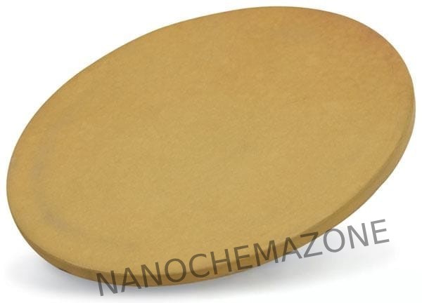
Silicon (Si) Sputtering Targets, N-type, Purity: 99.999%, Size: 5”, Thickness: 0.125”

$451.00

Product 

Silicon (Si) Sputtering Targets, N-type, Purity: 99.999%, Size: 5'', Thickness: 0.125''

CAS No.
7440-21-3

Appearance

Powder

Purity

≥99%,  ≥99.9%,  ≥95%

(Other purities are also available)

APS

N/A  (Size Can be customized), Ask for other available size ranges.

Ingredient

N/A

Molecular Weight

28.0855 g/mol

Melting Point

 1,414 °C

Boiling Point

3,265 °C

Density

 2.33 g/cm³

Product Codes

NCZ-1759K