• CONTACT US
  • FAQs
FREE SHIPPING WITHIN CANADA FOR ALL ORDER OF 300$
0 Compare
0 Wishlist
Login / Register
  • Home
  • Products
  • Contact Us
Menu
0 items / $0.00
Browse Categories
  • 3D Printer Materials
  • BATTERY EQUIPMENT
  • CARBON NANOTUBES
  • DISPERSIONS
  • MICROPARTICLES
  • MXene and MAXene
  • NANOPARTICLES & NANOPOWDERS
  • RARE EARTH MATERIALS
  • SILICON WAFERS & SEMICONDUCTOR WAFERS
24/7 SUPPORT

+1-780-612-4177

0 items / $0.00
Click to enlarge
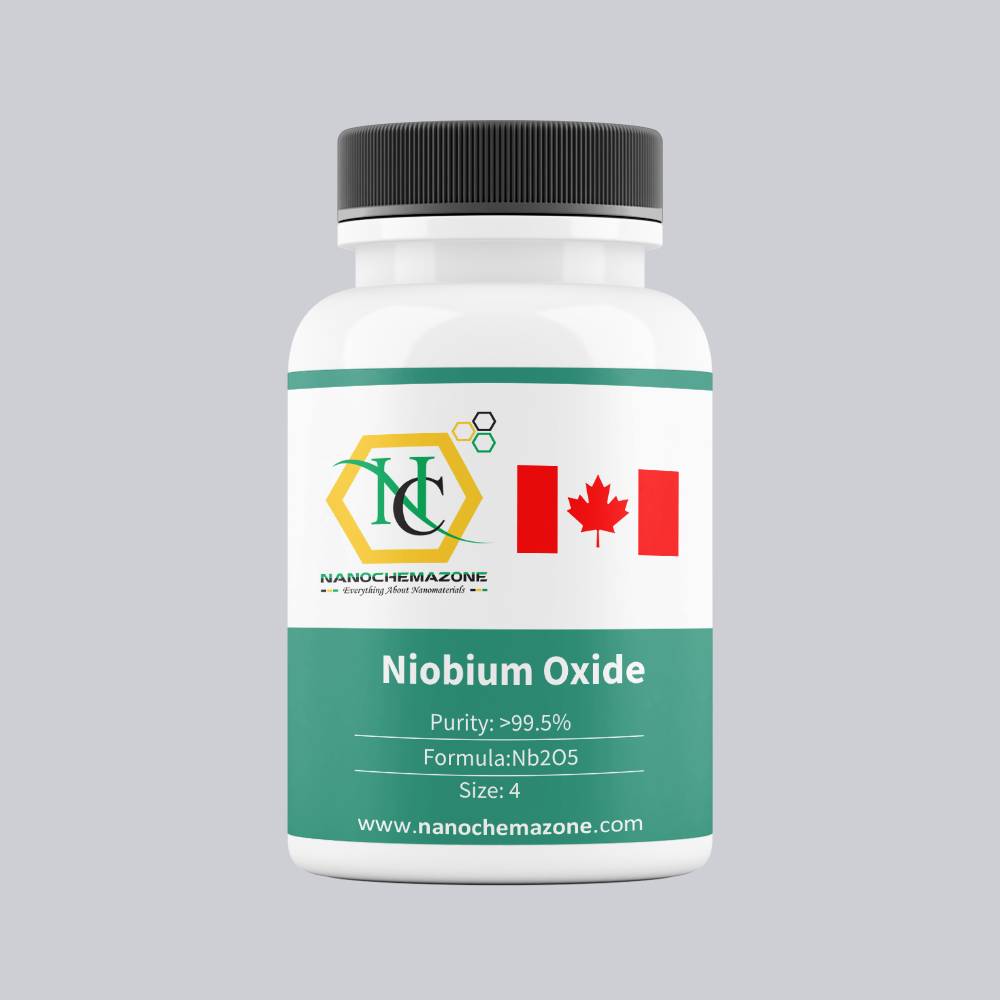
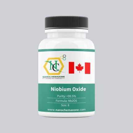
HomeSputtering TargetsSPUTTERING TARGETS NAMES N - SNIOBIUM OXIDE SPUTTERING TARGETS4 Niobium Oxide (Nb2O5) Sputtering Targets, Purity: 99.5%, Size: 4”, Thickness: 0.125”
Previous product
Niobium Oxide (Nb2O5) Sputtering Targets, Purity: 99.5%, Size: 4'', Thickness: 0.250'' $552.00
Back to products
Next product
Niobium Oxide (Nb2O5) Sputtering Targets, Purity: 99.5%, Size: 8'', Thickness: 0.250'' $516.00

Niobium Oxide (Nb2O5) Sputtering Targets, Purity: 99.5%, Size: 4”, Thickness: 0.125”

$442.00

Applications of Sputtering Targets;

Film deposition is accomplished using sputtering targets. A technique for sputtering thin films is called “deposition made by sputter targets,” which entails eroding material from a “target” source onto a “substrate” like a silicon wafer.
Etching of the target is done using semiconductor sputtering targets. When selectivity is not an issue and a high degree of etching anisotropy is required, sputter etching is the method of choice.
By removing the target material through etching, sputter targets are also utilized for investigation.
In secondary ion spectroscopy (SIMS), one example is when the target material is sputtered at a steady pace. Mass spectrometry is used to quantify the concentration and identity of spewed atoms as the target is sputtered.

The target material’s composition may be ascertained and even very low concentrations of contaminants can be found with the aid of the sputtering target.

There is also an application area for sputtering targets in space. One type of space weathering that alters the chemical and physical characteristics of airless worlds like the Moon and asteroids is sputtering.

Compare
Add to wishlist
Categories: 4, BATTERY EQUIPMENT, NIOBIUM OXIDE SPUTTERING TARGETS, Sputtering Targets, SPUTTERING TARGETS NAMES N - S
Share
  • Description
  • Shipping & Delivery
Description

Niobium Oxide (Nb2O5) Sputtering Targets

Purity: 99.5%, Size: 4”, Thickness: 0.125”

Sputtering is a well-established technique that can deposit thin films made of a wide range of materials on a variety of shaped and sized substrates.
Sputter targets allow for reproducible processes that can be expanded from small-scale R&D initiatives. Sputter target processes can be modified to suit medium- to large-sized substrate surfaces in manufacturing batches. Depending on the process settings, the chemical reaction may take place on the substrate, in flight, or on the target surface. Sputter deposition is a complicated process due to its numerous characteristics, yet professionals have a great deal of control over the region’s growth and microstructure.

Shipping & Delivery

Related products

Placeholder
Placeholder

Lithium Cobalt Oxide (LiCoO2) Powder for Li-ion Battery Cathode Application

BATTERY EQUIPMENT, RAW MATERIALS FOR BATTERY APPLICATION
$68.00 – $367.00
Select options
Compare
Quick view
Add to wishlist
Close
Placeholder
Placeholder

Nickel Hydroxide Ni(OH)2 (NiOH-Co) Micron Powder, Size: 10-15 µm, Spherical

BATTERY EQUIPMENT, RAW MATERIALS FOR BATTERY APPLICATION
$60.00 – $307.00
Select options
Compare
Quick view
Add to wishlist
Close
Placeholder
Placeholder

Lithium Iron Phosphate (LiFePO4) Powder for Li-ion Battery Cathode Application

BATTERY EQUIPMENT, RAW MATERIALS FOR BATTERY APPLICATION
$60.00 – $215.00
Select options
Compare
Quick view
Add to wishlist
Close

Graphite Sheet Thermal Interface Material, EYG Series, 1600 W/m.K, Thickness: 25 µm, Lenght: 180 mm, Width: 115 mm

BATTERY EQUIPMENT, FOILS FOR BATTERIES, Graphite Foils
$59.00 – $243.00
Select options
Compare
Quick view
Add to wishlist
Close
Placeholder
Placeholder

High Purity Natural Graphite Nanopowder/Nanoparticles for Li-ion Battery, Purity: 99.99+%, Size: 30 nm

BATTERY EQUIPMENT, RAW MATERIALS FOR BATTERY APPLICATION
$82.00 – $2,062.00
Select options
Compare
Quick view
Add to wishlist
Close

Graphite Sheet Thermal Interface Material, EYG Series, 1600 W/m.K, Thickness: 25 µm, Lenght: 230 mm, Width: 180 mm

BATTERY EQUIPMENT, FOILS FOR BATTERIES, Graphite Foils
$99.00 – $432.00
Select options
Compare
Quick view
Add to wishlist
Close

Graphite Sheet Thermal Interface Material, EYG Series, 1350 W/m.K, Thickness: 40 µm, Lenght: 115 mm, Width: 90 mm

BATTERY EQUIPMENT, FOILS FOR BATTERIES, Graphite Foils
$57.00 – $235.00
Select options
Compare
Quick view
Add to wishlist
Close

Graphene Nanoplatelet, Purity: 99.9+%, Size: 5 nm, S.A: 170 m2/g, Dia: 30 μm

BATTERY EQUIPMENT, RAW MATERIALS FOR BATTERY APPLICATION
$12.00 – $968.00
Select options
Compare
Quick view
Add to wishlist
Close

FREE SHIPPING

Carrier information.

ONLINE PAYMENT

Payment methods.

24/7 SUPPORT

Unlimited help desk.

100% SAFE

View our benefits.

FREE RETURNS

Track or cancel orders.

  • QUICK LINKS
    • About Us
    • Catalogue
    • Quotation
    • FAQ's
    • Products

  • CATEGORIES
    • MXene and MAXene
    • Wafers
    • Nanoparticles
    • Advanced Nanomaterials
    • Artificial Biological Solutions

  • POLICIES
    • Privacy Policy
    • Returns
    • Terms & Conditions
    • Contact Us
    • Our Sitemap

AVAILABLE ON:

Payment System:
payment
Shipping System:
shipping

©NANOCHEMAZONE @ 2015-24 | All Rights Reserved
  • Menu
  • Categories
  • 3D Printer Materials
  • BATTERY EQUIPMENT
  • CARBON NANOTUBES
  • DISPERSIONS
  • MICROPARTICLES
  • MXene and MAXene
  • NANOPARTICLES & NANOPOWDERS
  • RARE EARTH MATERIALS
  • SILICON WAFERS & SEMICONDUCTOR WAFERS
  • Home
  • Shop
  • Blog
  • About us
  • Wishlist
  • Compare
  • Login / Register
Shopping cart
close

Sign in

close

Lost your password?

No account yet?

Create an Account
Shop
0 Wishlist
0 items Cart
My account