High Purity (>99.9%) Fullerene-C60, 1g

$425.00
Product High Purity (>99.9%) Fullerene-C60, 1g
CAS No. 99685-96-8
Appearance Dark brown to black crystalline
Purity ≥99%,  ≥99.9%,  ≥95%(Other purities are also available)
APS N/A
Ingredient C₆₀
Molecular Weight 720.64 g/mol
Melting Point 290 °C
Boiling Point N/A
Density 1.65 g/cm³
Product Codes NCZ-394I
 

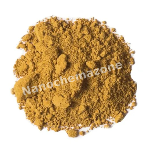
Indium Tin Oxide (ITO, 90:10wt%) Yellow Nanopowder 99.99% (4N), 100g

$425.00
Product Indium Tin Oxide (ITO, 90:10wt%) Yellow Nanopowder 99.99% (4N), 100g
CAS No. 1312-43-2
Appearance Yellow
Purity ≥99%,  ≥99.9%,  ≥95%(Other purities are also available)
APS 100nm (Size Can be customized),  Ask for other available size range.
Ingredient In2−xSnxO​
Molecular Weight 262–270 g/mol
Melting Point N/A
Boiling Point N/A
Density 7.14 g/cm³
Product Codes NCZ-426I

Lutetium (III) Oxide (Lu2O3) 99.995% 4N5 Powder

Price range: $425.00 through $3,236.00
Select options This product has multiple variants. The options may be chosen on the product page
Product Lutetium (III) Oxide (Lu2O3) 99.995% 4N5 Powder
CAS No. 12032-20-1
Appearance White to off-white
Purity ≥99%,  ≥99.9%,  ≥95%(Other purities are also available)
APS 100nm (Size Can be customized),  Ask for other available size range.
Ingredient Lu2O3
Molecular Weight 397.93 g/mol
Melting Point 2,490 °C
Boiling Point N/A
Density 9.42 g/cm³
Product Codes NCZ-448I
 

Yttrium Chloride Hexahydrate (YCl3 · 6H2O) 99.9% 3N

$425.00
Select options This product has multiple variants. The options may be chosen on the product page
Product Yttrium Chloride Hexahydrate (YCl3 · 6H2O) 99.9% 3N
CAS No. 10025-91-9
Appearance White crystalline powder or granules
Purity ≥99%,  ≥99.9%,  ≥95%(Other purities are also available)
APS N/A
Ingredient YCl3·6H2O
Molecular Weight 241.46 g/mol
Melting Point N/A
Boiling Point N/A
Density N/A
Product Codes NCZ-604I
 

Sodium ascorbyl phosphate(Cosmetic grade) (540513)

$425.00
Select options This product has multiple variants. The options may be chosen on the product page
Magnesium ascorbyl phosphate(Cosmetic grade) (539640)
      Synonym Vitamin C magnesium phosphate, Magnesium L-Ascorbyl Phosphate Structure
Molecular Formula C12H12O18P2Mg3·10H2O

TEST SPECIFICATIONS
1. Appearance White to pale yellow powder
2. Assay ≥98.50%
3. Loss on Drying ≤20%
4. Heavy metals(Pb) ≤0.001%
5. Arsenic ≤0.0002%
6. pH(3%aqueous solution) 7.0-8.5
7. State of solution(3% aqueous solution Colorless to pale yellowish transparent
8. Color of solution(APHA) ≤70
9. Free ascorbic acid ≤0.5%
10. Free Phosphoric acid ≤1%
11. Ketogulonic acid and its derivatives ≤2.5%
12. Derivatives of ascorbic acid ≤3.5 %
13. Chloride ≤0.35%
14. Total aerobic coumt ≤100 per gram
15. Packaging 1 kg aluminum foil bag, 5/10kg carton, 25 kg barrel, according to customer requirements
16. Shelf life 3 yr after production
Product Codes- NCZ-2709K

Lanthanum Strontium Manganate (La0.9Sr0.1MnO3) Sputtering Targets, Purity: 99.9%, Size: 2”, Thickness: 0.125”

$426.00

Applications of Sputtering Targets;

  • Sputtering targets is used for film deposition. The deposition made by sputter targets is a method of depositing thin films by sputtering that involves eroding material from a "target" source onto a "substrate" such as  a silicon wafer.
  • Semiconductor sputtering targets is used to etch the target. Sputter etching is chosen in cases where a high degree of etching anisotropy is needed and selectivity is not a concern.
  • Sputter targets is also used for analysis by etching away the target material.
One of the example occurs in secondary ion spectroscopy (SIMS), where the target sample is sputtered at a constant rate. As the target is sputtered, the concentration and identity of sputtered atoms are measured using mass spectrometry. By helping of the sputtering target, the composition of the target material can be determined and even extremely low concentrations of impurities are detected. Sputtering target has also application area in space. Sputtering is one of the forms of space weathering, a process that changes the physical and chemical properties of airless bodies, such as asteroids and the Moon.

Molybdenum Oxide (MoO3) Sputtering Targets, Purity: 99.9%, Size: 3”, Thickness: 0.250”

$426.00

Applications of Sputtering Targets;

Film deposition is accomplished using sputtering targets. A technique for sputtering thin films is called "deposition made by sputter targets," which entails eroding material from a "target" source onto a "substrate" like a silicon wafer. Etching of the target is done using semiconductor sputtering targets. When selectivity is not an issue and a high degree of etching anisotropy is required, sputter etching is the method of choice. By removing the target material through etching, sputter targets are also utilized for investigation. In secondary ion spectroscopy (SIMS), one example is when the target material is sputtered at a steady pace. Mass spectrometry is used to quantify the concentration and identity of spewed atoms as the target is sputtered.

The composition of the target material can be assessed and even minuscule levels of impurities can be identified with the aid of the sputtering target.

Applications to sputtering targets in space are also possible. Sputtering is one kind of space weathering that modifies the chemical and physical properties of airless worlds such as asteroids and the Moon.

Silicon (Si) Sputtering Targets, N-type, Purity: 99.999%, Size: 6”, Thickness: 0.250”

$426.00

Applications of Sputtering Targets;

Film deposition is accomplished using sputtering targets. A technique for sputtering thin films is called "deposition made by sputter targets," which entails eroding material from a "target" source onto a "substrate" like a silicon wafer. Etching of the target is done using semiconductor sputtering targets. When selectivity is not an issue and a high degree of etching anisotropy is required, sputter etching is the method of choice. By removing the target material through etching, sputter targets are also utilized for investigation. In secondary ion spectroscopy (SIMS), one example is when the target material is sputtered at a steady pace. Mass spectrometry is used to quantify the concentration and identity of spewed atoms as the target is sputtered.

The target material's composition may be ascertained and even very low concentrations of contaminants can be found with the aid of the sputtering target.

There is also an application area for sputtering targets in space. One type of space weathering that alters the chemical and physical characteristics of airless worlds like the Moon and asteroids is sputtering.

Gadolinium Sputtering Target Gd

$426.00
Select options This product has multiple variants. The options may be chosen on the product page
Product Gadolinium Sputtering Target Gd
CAS No. 7440-54-2
Appearance Solid, silvery-white metallic with slight oxidation tendency
Purity ≥99%,  ≥99.9%,  ≥95%(Other purities are also available)
APS N/A
Ingredient Gd
Molecular Weight 157.25 g/mol
Melting Point 1312 °C
Boiling Point 3273 °C
Density 7.90 g/cm³
Product Codes NCZ-114H

Molybdenum Oxide (MoO3) Sputtering Targets, Purity: 99.9%, Size: 2”, Thickness: 0.250”

$426.00

Product 

Molybdenum Oxide (MoO3) Sputtering Targets, Purity: 99.9%, Size: 2'', Thickness: 0.250''

CAS No.

1313-27-5

Appearance

Powder

Purity

≥99%,  ≥99.9%,  ≥95%

(Other purities are also available)

APS

 N/A (Size Can be customized), Ask for other available size ranges.

Ingredient

N/A

Molecular Weight

 143.94 g/mol

Melting Point

 ~795°C

Boiling Point

 ~1155°C

Density

 ~4.7 g/cm³

Product Codes

NCZ-1902K

Carbon (C) (Pyrolytic Graphite) Sputtering Targets, Purity: 99.999%, Size: 4”, Thickness: 0.125”

$427.00

Applications of Sputtering Targets;

Film deposition is accomplished using sputtering targets. A technique for sputtering thin films is called "deposition made by sputter targets," which entails eroding material from a "target" source onto a "substrate" like a silicon wafer. Etching of the target is done using semiconductor sputtering targets. When selectivity is not an issue and a high degree of etching anisotropy is required, sputter etching is the method of choice. By removing the target material through etching, sputter targets are also utilized for investigation. In secondary ion spectroscopy (SIMS), one example is when the target material is sputtered at a steady pace. Mass spectrometry is used to quantify the concentration and identity of spewed atoms as the target is sputtered.

The target material's composition may be ascertained and even very low concentrations of contaminants can be found with the aid of the sputtering target.

There is also an application area for sputtering targets in space. One type of space weathering that alters the chemical and physical characteristics of airless worlds like the Moon and asteroids is sputtering.

Carbon (C) (Pyrolytic Graphite) Sputtering Targets, Purity: 99.999%, Size: 4”, Thickness: 0.125”

$427.00

Applications of Sputtering Targets;

Film deposition is accomplished using sputtering targets. A technique for sputtering thin films is called "deposition made by sputter targets," which entails eroding material from a "target" source onto a "substrate" like a silicon wafer. Etching of the target is done using semiconductor sputtering targets. When selectivity is not an issue and a high degree of etching anisotropy is required, sputter etching is the method of choice. By removing the target material through etching, sputter targets are also utilized for investigation. In secondary ion spectroscopy (SIMS), one example is when the target material is sputtered at a steady pace. Mass spectrometry is used to quantify the concentration and identity of spewed atoms as the target is sputtered.

The target material's composition may be ascertained and even very low concentrations of contaminants can be found with the aid of the sputtering target.

There is also an application area for sputtering targets in space. One type of space weathering that alters the chemical and physical characteristics of airless worlds like the Moon and asteroids is sputtering.

Nickel (Ni) Sputtering Targets, Purity: 99.995%, Size: 6”, Thickness: 0.125”

$427.00

Applications of Sputtering Targets;

Film deposition is accomplished using sputtering targets. A technique for sputtering thin films is called "deposition made by sputter targets," which entails eroding material from a "target" source onto a "substrate" like a silicon wafer. Etching of the target is done using semiconductor sputtering targets. When selectivity is not an issue and a high degree of etching anisotropy is required, sputter etching is the method of choice. By removing the target material through etching, sputter targets are also utilized for investigation. In secondary ion spectroscopy (SIMS), one example is when the target material is sputtered at a steady pace. Mass spectrometry is used to quantify the concentration and identity of spewed atoms as the target is sputtered.

The target material's composition may be ascertained and even very low concentrations of contaminants can be found with the aid of the sputtering target.

There is also an application area for sputtering targets in space. One type of space weathering that alters the chemical and physical characteristics of airless worlds like the Moon and asteroids is sputtering.

Lanthanum Aluminate (LaAlO3) Sputtering Target

Price range: $427.00 through $928.00
Select options This product has multiple variants. The options may be chosen on the product page

Product 

Lanthanum Aluminate (LaAlO3) Sputtering Target

CAS No.

12003-62-4

Appearance

Powder

Purity

≥99%,  ≥99.9%,  ≥95%

(Other purities are also available)

APS

 NA (Size Can be customized), Ask for other available size ranges.

Ingredient

N/A

Molecular Weight

221.89 g/mol

Melting Point

~2,078 °C

Boiling Point

N\A

Density

~6.52 g/cm³

Product Codes

NCZ-1317K

Ytterbium Oxide (Yb2O3) Powder 99.999% 5N, High Purity, 100g

$427.00
Product Ytterbium Oxide (Yb2O3) Powder 99.999% 5N, High Purity, 100g
CAS No. 1314-37-0
Appearance White
Purity ≥99%,  ≥99.9%,  ≥95%(Other purities are also available)
APS 5µm (Size Can be customized),  Ask for other available size range.
Ingredient Yb2O3
Molecular Weight 394.08 g/mol
Melting Point 2,345 °C
Boiling Point 4,300 °C
Density N/A
Product Codes NCZ-599I

Nickel Chromium (Ni-Cr) Sputtering Targets, Purity: 99.95%, Size: 3”, Thickness: 0.250”

$428.00

Applications of Sputtering Targets;

Film deposition is accomplished using sputtering targets. A technique for sputtering thin films is called "deposition made by sputter targets," which entails eroding material from a "target" source onto a "substrate" like a silicon wafer. Etching of the target is done using semiconductor sputtering targets. When selectivity is not an issue and a high degree of etching anisotropy is required, sputter etching is the method of choice. By removing the target material through etching, sputter targets are also utilized for investigation. In secondary ion spectroscopy (SIMS), one example is when the target material is sputtered at a steady pace. Mass spectrometry is used to quantify the concentration and identity of spewed atoms as the target is sputtered.

The target material's composition may be ascertained and even very low concentrations of contaminants can be found with the aid of the sputtering target.

There is also an application area for sputtering targets in space. One type of space weathering that alters the chemical and physical characteristics of airless worlds like the Moon and asteroids is sputtering.

Holmium (Ho) Sputtering Target

Price range: $428.00 through $1,020.00
Select options This product has multiple variants. The options may be chosen on the product page

Product 

Holmium (Ho) Sputtering Target

CAS No.

7440-60-0

Appearance

Powder

Purity

≥99%,  ≥99.9%,  ≥95%

(Other purities are also available)

APS

 NA (Size Can be customized), Ask for other available size ranges.

Ingredient

N/A

Molecular Weight

164.930 g/mol

Melting Point

1,474 °C

Boiling Point

2,700 °C

Density

8.80 g/cm³

Product Codes

NCZ-1292K

Molybdenum Disulfide (MoS2) Sputtering Targets, Purity: 99.9%, Size: 1”, Thickness: 0.250”

$428.00

Product 

Molybdenum Disulfide (MoS2) Sputtering Targets, Purity: 99.9%, Size: 1'', Thickness: 0.250''

CAS No.

 1317-33-5

Appearance

Powder

Purity

≥99%,  ≥99.9%,  ≥95%

(Other purities are also available)

APS

 N/A (Size Can be customized), Ask for other available size ranges.

Ingredient

N/A

Molecular Weight

 160.07 g/mol

Melting Point

 ~1185 °C

Boiling Point

 ~4500 °C

Density

 ~5.06 g/cm³

Product Codes

NCZ-1918K

Iron Oxide (Fe3O4) Sputtering Targets, Purity: 99.9%, Size: 1”, Thickness: 0.125”

$429.00

Applications of Sputtering Targets;

Film deposition is accomplished using sputtering targets. A technique for sputtering thin films is called "deposition made by sputter targets," which entails eroding material from a "target" source onto a "substrate" like a silicon wafer. Etching of the target is done using semiconductor sputtering targets. When selectivity is not an issue and a high degree of etching anisotropy is required, sputter etching is the method of choice. By removing the target material through etching, sputter targets are also utilized for investigation. In secondary ion spectroscopy (SIMS), one example is when the target material is sputtered at a steady pace. Mass spectrometry is used to quantify the concentration and identity of spewed atoms as the target is sputtered.

The target material's composition may be ascertained and even very low concentrations of contaminants can be found with the aid of the sputtering target.

There is also an application area for sputtering targets in space. One type of space weathering that alters the chemical and physical characteristics of airless worlds like the Moon and asteroids is sputtering.

Vanadium (V) Sputtering Targets, Purity: 99.5%, Size: 4”, Thickness: 0.125”

$429.00

Applications of Sputtering Targets;

Film deposition is accomplished using sputtering targets. A technique for sputtering thin films is called "deposition made by sputter targets," which entails eroding material from a "target" source onto a "substrate" like a silicon wafer. Etching of the target is done using semiconductor sputtering targets. When selectivity is not an issue and a high degree of etching anisotropy is required, sputter etching is the method of choice. By removing the target material through etching, sputter targets are also utilized for investigation. In secondary ion spectroscopy (SIMS), one example is when the target material is sputtered at a steady pace. Mass spectrometry is used to quantify the concentration and identity of spewed atoms as the target is sputtered.

The target material's composition may be ascertained and even very low concentrations of contaminants can be found with the aid of the sputtering target.

There is also an application area for sputtering targets in space. One type of space weathering that alters the chemical and physical characteristics of airless worlds like the Moon and asteroids is sputtering.

3N (99.9%) Ytterbium Fluoride (YbF3) Pieces (1-6mm) Evaporation Materials

Price range: $429.00 through $924.00
Select options This product has multiple variants. The options may be chosen on the product page
Product 3N (99.9%) Ytterbium Fluoride (YbF3) Pieces (1-6mm) Evaporation Materials
CAS No. 13760-80-0
Appearance White, Crystalline Solid
Purity ≥99%,  ≥99.9%,  ≥95%(Other purities are also available)
APS 1-6mm (Size Can be customized),  Ask for other available size range.
Ingredient YbF3
Molecular Weight 230.04 g/mol
Melting Point 1,157 °C
Boiling Point N/A
Density 8.2 g/cm3
Product Codes NCZ-168E

Nickel/Chromium (Ni/Cr 80/20 wt.%) Pellets (6mm Diameter x 6mm Length) Evaporation Materials

Price range: $429.00 through $924.00
Select options This product has multiple variants. The options may be chosen on the product page
Product Nickel/Chromium (Ni/Cr 80/20 wt.%) Pellets (6mm Diameter x 6mm Length) Evaporation Materials
CAS No. 1116-97-1
Appearance Silvery-gray, metallic gray
Purity ≥99%,  ≥99.9%,  ≥95%(Other purities are also available)
APS 6mm (Size Can be customized),  Ask for other available size range.
Ingredient Ni/Cr
Molecular Weight 57.35g/mol
Melting Point N/A
Boiling Point N/A
Density 8.4 g/cm3
Product Codes NCZ-169E

2.5 mL Palladium (Pd) Nanoparticles (15-25 nm) Water Dispersion, 1 mg/mL

$429.00
Product 2.5 mL Palladium (Pd) Nanoparticles (15-25 nm) Water Dispersion, 1 mg/mL
CAS No. 7440-05-3
Appearance Brown-black liquid
Purity ≥99%,  ≥99.9%,  ≥95%(Other purities are also available)
APS 15-25 nm (Size Can be customized),  Ask for other available size range.
Ingredient Pd
Molecular Weight N/A
Melting Point N/A
Boiling Point N/A
Density N/A
Product Codes NCZ-143I
 

Vanadium (V) Sputtering Targets, Purity: 99.5%, Size: 3”, Thickness: 0.250”

$429.00

Product 

Vanadium (V) Sputtering Targets, Purity: 99.5%, Size: 3'', Thickness: 0.250''

CAS No.

7440-62-2

Appearance

Powder

Purity

≥99%,  ≥99.9%,  ≥95%

(Other purities are also available)

APS

N/A  (Size Can be customized), Ask for other available size ranges.

Ingredient

N/A

Molecular Weight

50.9415 g/mol

Melting Point

1910 °C

Boiling Point

3407 °C

Density

6.11 g/cm³

Product Codes

NCZ-1547K

99.999% 5N 10-20 nm Gamma Aluminum Oxide (Alumina) Al2O3 Powder, 500 g

$429.00
Product 99.999% 5N 10-20 nm Gamma Aluminum Oxide (Alumina) Al2O3 Powder, 500 g
CAS No. 1344-28-1
Appearance White to off-white
Purity ≥99%,  ≥99.9%,  ≥95%(Other purities are also available)
APS 10-20nm (Size Can be customized),  Ask for other available size range.
Ingredient Al2O3
Molecular Weight 101.96 g/mol
Melting Point N/A
Boiling Point N/A
Density 3.65 g/cm³
Product Codes NCZ-257I

99.999% 5N Germanium (Ge) Powder, 100 Mesh

Price range: $429.00 through $1,298.00
Select options This product has multiple variants. The options may be chosen on the product page
Product 99.999% 5N Germanium (Ge) Powder, 100 Mesh
CAS No. 7440-56-4
Appearance Gray to dark gray fine
Purity ≥99%,  ≥99.9%,  ≥95%(Other purities are also available)
APS 149µm (Size Can be customized),  Ask for other available size range.
Ingredient Ge
Molecular Weight 72.63 g/mol
Melting Point N/A
Boiling Point N/A
Density 5.323 g/cm³
Product Codes NCZ-263I
 

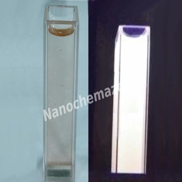
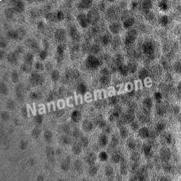
Alkylated Carbon Quantum Dot Powder (Blue Fluorescence), 100mg

$429.00
Product Alkylated Carbon Quantum Dot Powder (Blue Fluorescence), 100mg
CAS No. 7723-14-0
Appearance Brownish yellow
Purity ≥99%,  ≥99.9%,  ≥95%(Other purities are also available)
APS 2-6nm (Size Can be customized),  Ask for other available size range.
Ingredient CxHyOzRn​
Molecular Weight N/A
Melting Point N/A
Boiling Point N/A
Density 0.4–0.7 g/cm³
Product Codes NCZ-276I
 

Carboxymethyl Dextran Modified Fe3O4 Nanoparticle Water Dispersion, 4mg/mL

Price range: $429.00 through $825.00
Select options This product has multiple variants. The options may be chosen on the product page
Product Carboxymethyl Dextran Modified Fe3O4 Nanoparticle Water Dispersion, 4mg/mL
CAS No. 1317-61-9
Appearance Brown to black aqueous
Purity ≥99%,  ≥99.9%,  ≥95%(Other purities are also available)
APS 10–30nm (Size Can be customized),  Ask for other available size range.
Ingredient Fe3O4​
Molecular Weight N/A
Melting Point N/A
Boiling Point N/A
Density 5.2 g/cm³
Product Codes NCZ-310I
 

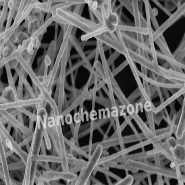
Copper (Cu) Nanowire Dispersion, 1g/bottle

$429.00
Select options This product has multiple variants. The options may be chosen on the product page
Product Copper (Cu) Nanowire Dispersion, 1g/bottle
CAS No. 7440-50-8
Appearance Reddish-brown to red suspension
Purity ≥99%,  ≥99.9%,  ≥95%(Other purities are also available)
APS 100–200nm (Size Can be customized),  Ask for other available size range.
Ingredient Cu
Molecular Weight 63.55 g/mol
Melting Point N/A
Boiling Point N/A
Density 8.96 g/cm³
Product Codes NCZ-330I

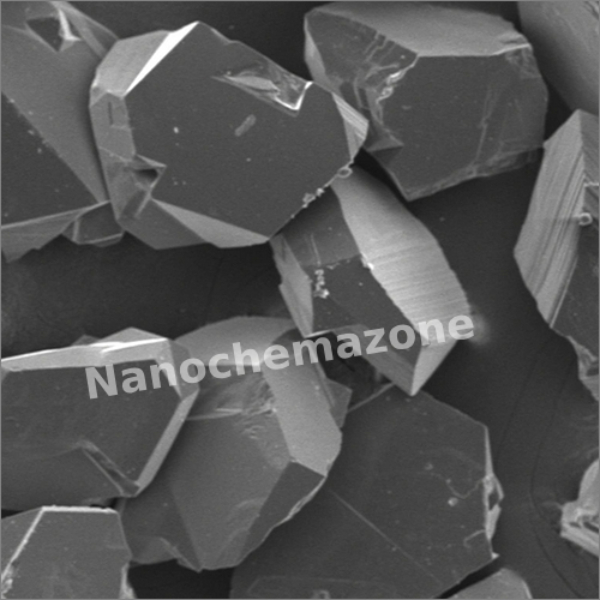
Cubic Boron Nitride (CBN) Superabrasive Micropowder

Price range: $429.00 through $836.00
Select options This product has multiple variants. The options may be chosen on the product page
Product Cubic Boron Nitride (CBN) Superabrasive Micropowder
CAS No. 10043-11-5
Appearance Black or dark gray
Purity ≥99%,  ≥99.9%,  ≥95%(Other purities are also available)
APS 0.5–1µm (Size Can be customized),  Ask for other available size range.
Ingredient Bn
Molecular Weight N/A
Melting Point N/A
Boiling Point N/A
Density 1.9 to 2.1 g/cm³
Product Codes NCZ-332I

Graphene Quantum Dots Powder (Red Fluorescence), 50mg

$429.00
Product Graphene Quantum Dots Powder (Red Fluorescence), 50mg
CAS No. 7440-44-0
Appearance Brownish-black
Purity ≥99%,  ≥99.9%,  ≥95%(Other purities are also available)
APS 10nm (Size Can be customized),  Ask for other available size range.
Ingredient CₓOᵧH_z
Molecular Weight 1000 g/mol
Melting Point N/A
Boiling Point N/A
Density N/A
Product Codes NCZ-365I

Graphene Quantum Dots Powder (White Fluorescence), 50mg

$429.00
Product Graphene Quantum Dots Powder (White Fluorescence), 50mg
CAS No. 7440-44-0
Appearance Light brown to grayish
Purity ≥99%,  ≥99.9%,  ≥95%(Other purities are also available)
APS 10nm (Size Can be customized),  Ask for other available size range.
Ingredient CₓOᵧH_z
Molecular Weight 300 g/mol
Melting Point N/A
Boiling Point N/A
Density 2.0–2.3 g/cm³
Product Codes NCZ-366I
 

Multilayer Titanium Carbonitride (Ti3CN) MXene Material

Price range: $429.00 through $1,419.00
Select options This product has multiple variants. The options may be chosen on the product page
Product Multilayer Titanium Carbonitride (Ti3CN) MXene Material
CAS No. 12316-56-2
Appearance Dark gray to black
Purity ≥99%,  ≥99.9%,  ≥95%(Other purities are also available)
APS 1-5um ( (Size Can be customized),  Ask for other available size range.
Ingredient Ti3CN
Molecular Weight 169.62 g/mol
Melting Point 350 °C
Boiling Point N/A
Density N/A
Product Codes NCZ-465I
 

Nitrogen-Doped Carbon-Iridium Single-Atom Catalyst, Ir-N-C SAC, 1g

$429.00
Product Nitrogen-Doped Carbon-Iridium Single-Atom Catalyst, Ir-N-C SAC, 1g
CAS No. N/A
Appearance Dark gray
Purity ≥99%,  ≥99.9%,  ≥95%(Other purities are also available)
APS 0.5–5µm (Size Can be customized),  Ask for other available size range.
Ingredient Ir–Nₓ–C
Molecular Weight N/A
Melting Point N/A
Boiling Point N/A
Density 0.3–0.6 g/cm³
Product Codes NCZ-483I
 

Polyaniline Rod Powder, 5g/bottle

$429.00
Product Polyaniline Rod Powder, 5g/bottle
CAS No. 25233-30-1
Appearance Dark green to black
Purity ≥99%,  ≥99.9%,  ≥95%(Other purities are also available)
APS 50–200nm (Size Can be customized),  Ask for other available size range.
Ingredient (C6H4NH)n​
Molecular Weight N/A
Melting Point N/A
Boiling Point N/A
Density 1.3–1.4 g/cm³
Product Codes NCZ-495I

Samarium Nitrate Hexahydrate (Sm(NO3)3 · 6H2O) 99.99% 4N

Price range: $429.00 through $755.00
Select options This product has multiple variants. The options may be chosen on the product page
Product Samarium Nitrate Hexahydrate (Sm(NO3)3 · 6H2O) 99.99% 4N
CAS No. 13759-83-6
Appearance Colorless to pale pink crystalline
Purity ≥99%,  ≥99.9%,  ≥95%(Other purities are also available)
APS 10–50 µm  .(Size Can be customized),  Ask for other available size range.
Ingredient Sm(NO3)3·6H2O
Molecular Weight 434.46 g/mol
Melting Point 2345 °C
Boiling Point N/A
Density 2.45 g/cm³
Product Codes NCZ-509I

Sulfur Quantum Dots Solution, 28 mg/mL

Price range: $429.00 through $759.00
Select options This product has multiple variants. The options may be chosen on the product page
Product Sulfur Quantum Dots Solution, 28 mg/mL
CAS No. N/A
Appearance Clear to slightly yellow or light brown
Purity ≥99%,  ≥99.9%,  ≥95%(Other purities are also available)
APS 10nm (Size Can be customized),  Ask for other available size range.
Ingredient Sₓ
Molecular Weight N/A
Melting Point N/A
Boiling Point N/A
Density N/A
Product Codes NCZ-544I

Indium (In) Sputtering Targets, Purity: 99.99%, Size: 3”, Thickness: 0.125”

$429.00

Product 

Indium (In) Sputtering Targets, Purity: 99.99%, Size: 3'', Thickness: 0.125''

CAS No.

 7440-74-6

Appearance

Powder

Purity

≥99%,  ≥99.9%,  ≥95%

(Other purities are also available)

APS

 N/A (Size Can be customized), Ask for other available size ranges.

Ingredient

N/A

Molecular Weight

114.82 g/mol

Melting Point

 156.6 °C

Boiling Point

 2,072 °C

Density

 7.31 g/cm³

Product Codes

NCZ-2227K

Aluminum Nitride (AlN) Sputtering Targets, Purity: 99.8%, Size: 1”, Thickness: 0.125”

$429.00

Product 

Aluminum Nitride (AlN) Sputtering Targets, Purity: 99.8%, Size: 1'', Thickness: 0.125''

CAS No.

 24304-00-5

Appearance

Powder

Purity

≥99%,  ≥99.9%,  ≥95%

(Other purities are also available)

APS

N/A (Size Can be customized), Ask for other available size ranges.

Ingredient

N/A

Molecular Weight

40.99 g/mol

Melting Point

 ~2200 °C

Boiling Point

 N/A

Density

 ~3.26 g/cm³

Product Codes

NCZ-2561K

Silicon Carbide Wafer (SiC-4H) – 4H, Size: 3”, Thickness: 350 μm, Dummy Grade, 4H Area: 95%

Price range: $430.00 through $1,974.00
Select options This product has multiple variants. The options may be chosen on the product page
1 piece/390 € 5 pieces/1790 €                         Please contact us for quotes on larger quantities !!!

Silicon Carbide Wafer (SiC-4H)-4H

Size: 3'', Thickness: 350 μm, 4H Area: 95%

Technical Properties:

Quality  Dummy Grade
Size (inch)  3”
Thickness (μm)  350
Ra  ≤0.3
4H area  95%
Orientation  4°±0.5°
Resistivity   0.015-0.03
TTV  ≤15
Bow  ≤25
Warp  ≤35
OF Length  22.0±2.0
IF Length  11.0±1.5

Fields of Application for Silicon Carbide (SiC-4H)- 4H Wafer

Silicon carbide (SiC) is a rare compound of silicon and carbon which is synthetically produced. Silicon carbide (SiC) wafer has great electrical properties and excellent thermal properties. Silicon carbide (SiC) wafer has low thermal expansion. Silicon carbide (SiC) wafer has superior hardness properties. Silicon carbide (SiC) wafer performs well at high temperatures. Also, silicon carbide (SiC) wafer has high resistance to corrosion, erosion and oxidation. In addition to, silicon carbide (SiC) wafer is also more shiny than either diamonds or cubic zirconia. Silicon carbide (SiC) crystals have unique physical and electronic properties. Silicon Carbide based devices have been used for short wavelength opto-electronic, high temperature, radiation resistant applications.  The high-power and high-frequency electronic devices made with SiC are superior to Si and GaAs based devices.  Below are some popular applications of SiC substrates. SiC based devices have low lattice mismatch with III-nitride epitaxial layers.  They have high thermal conductivity and can be used for the monitoring of combustion processes and for all sorts of UV-detection.  SiC-based semiconductor devices can work under very hostile environments, such as high temperature, high power, and high radiation conditions. SiC is used for the fabrication of very high-voltage and high-power devices such as diodes, power transistors, and high power microwave devices. Compared to conventional Si-devices, SiC-based power devices have faster switching speed higher voltages, lower parasitic resistances, smaller size, less cooling required due to high-temperature capability. While Silicon carbide (SiC-4H)- 4H wafer has superior electronic properties, silicon carbide (SiC-6H)– 6H wafer is most easily prepared and best studied.
  • Silicon carbide (SiC) wafer is used for hybrid and electric vehicles.
  • Silicon carbide (SiC) wafer is used for green energy generation.
  • Silicon carbide (SiC) wafer is used for LEDs.
  • Silicon carbide (SiC) wafer is used for many other emerging markets.

Antimony (Sb) Sputtering Targets, Purity: 99.999%, Size: 3”, Thickness: 0.125”

$430.00

Product 

Antimony (Sb) Sputtering Targets, Purity: 99.999%, Size: 3'', Thickness: 0.125''

CAS No.

 7440-36-0

Appearance

Powder

Purity

≥99%,  ≥99.9%,  ≥95%

(Other purities are also available)

APS

N/A (Size Can be customized), Ask for other available size ranges.

Ingredient

N/A

Molecular Weight

 121.76 g/mol

Melting Point

 630.6 °C

Boiling Point

 1587 °C

Density

 6.69 g/cm³

Product Codes

NCZ-2506K

Lanthanum Calcium Manganate (La0.7Ca0.3MnO3) Sputtering Targets, Purity: 99.9%, Size: 3”, Thickness: 0.250”

$431.00
Select options This product has multiple variants. The options may be chosen on the product page

Applications of Sputtering Targets;

  • Sputtering targets is used for film deposition. The deposition made by sputter targets is a method of depositing thin films by sputtering that involves eroding material from a "target" source onto a "substrate" such as  a silicon wafer.
  • Semiconductor sputtering targets is used to etch the target. Sputter etching is chosen in cases where a high degree of etching anisotropy is needed and selectivity is not a concern.
  • Sputter targets is also used for analysis by etching away the target material.
One of the example occurs in secondary ion spectroscopy (SIMS), where the target sample is sputtered at a constant rate. As the target is sputtered, the concentration and identity of sputtered atoms are measured using mass spectrometry. By helping of the sputtering target, the composition of the target material can be determined and even extremely low concentrations of impurities are detected. Sputtering target has also application area in space. Sputtering is one of the forms of space weathering, a process that changes the physical and chemical properties of airless bodies, such as asteroids and the Moon.

Lanthanum Calcium Manganate (La0.7Ca0.3MnO3) Sputtering Targets, Purity: 99.9%, Size: 3”, Thickness: 0.250”

$431.00

Applications of Sputtering Targets;

Film deposition is accomplished using sputtering targets. A technique for sputtering thin films is called "deposition made by sputter targets," which entails eroding material from a "target" source onto a "substrate" like a silicon wafer. Etching of the target is done using semiconductor sputtering targets. When selectivity is not an issue and a high degree of etching anisotropy is required, sputter etching is the method of choice. By removing the target material through etching, sputter targets are also utilized for investigation. In secondary ion spectroscopy (SIMS), one example is when the target material is sputtered at a steady pace. Mass spectrometry is used to quantify the concentration and identity of spewed atoms as the target is sputtered.

The target material's composition may be ascertained and even very low concentrations of contaminants can be found with the aid of the sputtering target.

There is also an application area for sputtering targets in space. One type of space weathering that alters the chemical and physical characteristics of airless worlds like the Moon and asteroids is sputtering.

Silicon Dioxide (SiO2) Sputtering Targets, Fused Quartz, indium, Purity: 99.995%, Size: 2”, Thickness: 0.125”

$431.00

Product 

Silicon Dioxide (SiO2) Sputtering Targets, Fused Quartz, indium, Purity: 99.995%, Size: 2'', Thickness: 0.125''

CAS No.

60676-86-0

Appearance

Powder

Purity

≥99%,  ≥99.9%,  ≥95%

(Other purities are also available)

APS

N/A  (Size Can be customized), Ask for other available size ranges.

Ingredient

N/A

Molecular Weight

60.08 g/mol

Melting Point

~1715 °C

Boiling Point

~2230 °C

Density

~2.20 g/cm³

Product Codes

NCZ-1708K

Shape Memory Polymer NGM7520, Ether Type

Price range: $432.00 through $5,988.00
Select options This product has multiple variants. The options may be chosen on the product page

Applications:

Shape Memory Polymer (SMP) has myriad of advanced applications in different fields from daily life uses like textile to biomedicals. These applications include smart catheter, drug-delivery systems, biosensors, auto-repairing automobile parts, smart textile, self-healing materials, smart suture, artificial organs like muscles, and so on.

Shape Memory Polymer NGS2520, Solution Type

Price range: $432.00 through $6,232.00
Select options This product has multiple variants. The options may be chosen on the product page

Applications:

Shape Memory Polymer (SMP) has myriad of advanced applications in different fields from daily life uses like textile to biomedicals. These applications include smart catheter, drug-delivery systems, biosensors, auto-repairing automobile parts, smart textile, self-healing materials, smart suture, artificial organs like muscles, and so on.

Indium Phosphide (InP) Wafers, Size: 2”, Thickness: 350± 25 μm, Orientation: 111, Single Side Polished, EPI-Ready

Price range: $432.00 through $1,968.00
Select options This product has multiple variants. The options may be chosen on the product page
Indium Phosphide (InP) Wafers Size: 2”, Thickness: 350±25 μm, Orientation: 111 Technical Properties: Size (inch)  2” Thickness (μm)  350± 25 Dopant

Indium Phosphide (InP) Wafers, Size: 2”, Thickness: 350±25 μm, Orientation: 100, Single Side Polished, EPI-Ready

Price range: $432.00 through $1,968.00
Select options This product has multiple variants. The options may be chosen on the product page
Indium Phosphide (InP) Wafers Size: 2”, Thickness: 350±25 μm, Orientation: 100 Technical Properties: Size (inch)  2” Thickness (μm)  350± 25 Dopant

Tungsten Titanium (TiW) Sputtering Targets, Purity: 99.99%, Size: 8”, Thickness: 0.250”

$432.00

Applications of Sputtering Targets;

Film deposition is accomplished using sputtering targets. A technique for sputtering thin films is called "deposition made by sputter targets," which entails eroding material from a "target" source onto a "substrate" like a silicon wafer. Etching of the target is done using semiconductor sputtering targets. When selectivity is not an issue and a high degree of etching anisotropy is required, sputter etching is the method of choice. By removing the target material through etching, sputter targets are also utilized for investigation. In secondary ion spectroscopy (SIMS), one example is when the target material is sputtered at a steady pace. Mass spectrometry is used to quantify the concentration and identity of spewed atoms as the target is sputtered.

The target material's composition may be ascertained and even very low concentrations of contaminants can be found with the aid of the sputtering target.

There is also an application area for sputtering targets in space. One type of space weathering that alters the chemical and physical characteristics of airless worlds like the Moon and asteroids is sputtering.

Permalloy (Ni-Fe-Mo) Sputtering Targets, Size: 4”, Thickness: 0.125”

$432.00

Product 

Permalloy (Ni-Fe-Mo) Sputtering Targets, Size: 4'', Thickness: 0.125''

CAS No.

 Nickel: 7440-02-0 Iron: 7439-89-6 Molybdenum: 7439-98-7

Appearance

Powder

Purity

≥99%,  ≥99.9%,  ≥95%

(Other purities are also available)

APS

N/A (Size Can be customized), Ask for other available size ranges.

Ingredient

N/A

Molecular Weight

 Not defined (alloy), but elemental weights: Ni: 58.69 g/mol Fe: 55.85 g/mol Mo: 95.95 g/mol

Melting Point

 ~1450 °C

Boiling Point

 ~2730–3000 °C

Density

~8.7 g/cm³

Product Codes

NCZ-1797K

Indium (In) Sputtering Targets, Purity: 99.999%, Size: 2”, Thickness: 0.250”

$433.00

Product 

Indium (In) Sputtering Targets, Purity: 99.999%, Size: 2'', Thickness: 0.250''

CAS No.

 7440-74-6

Appearance

Powder

Purity

≥99%,  ≥99.9%,  ≥95%

(Other purities are also available)

APS

 N/A (Size Can be customized), Ask for other available size ranges.

Ingredient

N/A

Molecular Weight

114.82 g/mol

Melting Point

 156.6 °C

Boiling Point

 2,072 °C

Density

 7.31 g/cm³

Product Codes

NCZ-2228K

Magnesium (Mg) Sputtering Targets, Purity: 99.95%, Size: 6”, Thickness: 0.250”

$434.00

Applications of Sputtering Targets;

Film deposition is accomplished using sputtering targets. A technique for sputtering thin films is called "deposition made by sputter targets," which entails eroding material from a "target" source onto a "substrate" like a silicon wafer. Etching of the target is done using semiconductor sputtering targets. When selectivity is not an issue and a high degree of etching anisotropy is required, sputter etching is the method of choice. By removing the target material through etching, sputter targets are also utilized for investigation. In secondary ion spectroscopy (SIMS), one example is when the target material is sputtered at a steady pace. Mass spectrometry is used to quantify the concentration and identity of spewed atoms as the target is sputtered.

By helping of the sputtering target, the composition of the target material may be evaluated and even extremely tiny amounts of contaminants are recognized.

There is also an application area for sputtering targets in space. One type of space weathering that alters the chemical and physical characteristics of airless worlds like the Moon and asteroids is sputtering.

Copper-Carbon Nanotube Fibers Composite Wires, Cu-CNT, Diameter: 10-30 µm, Coating Thickness: 1 µm, Electrical conductivity: 1×10^7 S/m

Price range: $435.00 through $1,799.00
Select options This product has multiple variants. The options may be chosen on the product page
Copper-Carbon Nanotube Fibers Composite Wires Cu-CNT, Diameter: 10-30 µm, Coating Thickness: 1 µm, Electrical conductivity: 1x10⁷ S/m Copper/carbon nanotube composites (Cu/CNT composites) is produced for the demand of lighter copper substitutes with superior electrical, thermal and mechanical performances. They are used in many industries and vehicles such as automobiles and aircrafts in order to enhance fuel efficiencies. In electronics, they offer better interconnection and thermal management than copper with higher current- and heat-stabilities to enable device miniaturization with increased functionality. This material is highly functional, efficient, and sustainable for the next-generation electrical and electronics systems.

Monolayer Graphene on SiO2/Si Substrate, Size: 4″

Price range: $435.00 through $1,918.00
Select options This product has multiple variants. The options may be chosen on the product page

Applications:

Graphene research; Supercapacitors; Catalyst; Solar energy; Graphene optoelectronics, plasmonics and nanophotonics; Graphene semiconductor chips; Conductive graphene film; Graphene computer memory; Biomaterials and Bioelectronics.

Barium (Ba) Sputtering Targets, Purity: 99.5%, Size: 3”, Thickness: 0.250”

$435.00

Applications of Sputtering Targets;

Film deposition is accomplished using sputtering targets. A technique for sputtering thin films is called "deposition made by sputter targets," which entails eroding material from a "target" source onto a "substrate" like a silicon wafer. Etching of the target is done using semiconductor sputtering targets. When selectivity is not an issue and a high degree of etching anisotropy is required, sputter etching is the method of choice. By removing the target material through etching, sputter targets are also utilized for investigation. In secondary ion spectroscopy (SIMS), one example is when the target material is sputtered at a steady pace. Mass spectrometry is used to quantify the concentration and identity of spewed atoms as the target is sputtered. With the sputtering target's assistance, the

It is possible to identify the target material and even detect incredibly tiny impurity amounts.

There is also an application area for sputtering targets in space. One type of space weathering that alters the chemical and physical characteristics of airless worlds like the Moon and asteroids is sputtering.

A Block S, Group 2, Period 6 element with an atomic weight of 137.27, barium has the atomic symbol Ba and atomic number 56. One of the alkaline-earth metals is barium. Electronics can be plated using barium sputtering targets. Barium has favorable electrical characteristics.

Barium (Ba) Sputtering Targets, Purity: 99.5%, Size: 3”, Thickness: 0.125”

$435.00

Applications of Sputtering Targets;

Film deposition is accomplished using sputtering targets. A technique for sputtering thin films is called "deposition made by sputter targets," which entails eroding material from a "target" source onto a "substrate" like a silicon wafer. Etching of the target is done using semiconductor sputtering targets. When selectivity is not an issue and a high degree of etching anisotropy is required, sputter etching is the method of choice. By removing the target material through etching, sputter targets are also utilized for investigation. In secondary ion spectroscopy (SIMS), one example is when the target material is sputtered at a steady pace. When the target shatters,

Mass spectrometry measures the concentration and identity of sputtered atoms. The target material's composition may be ascertained and even very low concentrations of contaminants can be found with the aid of the sputtering target.

There is also an application area for sputtering targets in space. One type of space weathering that alters the chemical and physical characteristics of airless worlds like the Moon and asteroids is sputtering.

A Block S, Group 2, Period 6 element with an atomic weight of 137.27, barium has the atomic symbol Ba and atomic number 56. Barium is a mineral that an alkaline-earth metal member. Electronics can be plated using barium sputtering targets. Barium is beneficial for sputtering applications because of its good electrical characteristics. Barium sputtering targets can be utilized for semiconductors. Barium sputtering targets will work well for flat panel displays. Barium can be combined with other metals, such as titanium and strontium, to create alloys with more specialized qualities.

Aluminum Nitride (AlN) Sputtering Targets, Purity: 99.8%, Size: 1”, Thickness: 0.250”

$436.00

 Applications of Sputtering Targets;

  • Sputtering targets is used for film deposition. The deposition made by sputter targets is a method of depositing thin films by sputtering that involves eroding material from a "target" source onto a "substrate" such as  a silicon wafer.
  • Semiconductor sputtering targets is used to etch the target. Sputter etching is chosen in cases where a high degree of etching anisotropy is needed and selectivity is not a concern.
  • Sputter targets is also used for analysis by etching away the target material.
One of the example occurs in secondary ion spectroscopy (SIMS), where the target sample is sputtered at a constant rate. As the target is sputtered, the concentration and identity of sputtered atoms are measured using mass spectrometry. By helping of the sputtering target, the composition of the target material can be determined and even extremely low concentrations of impurities are detected. Sputtering target has also application area in space. Sputtering is one of the forms of space weathering, a process that changes the physical and chemical properties of airless bodies, such as asteroids and the Moon. Aluminum nitride is a chemical compound with the formula of AlN.Aluminum nitride has excellent combination of physical, chemical, and mechanical properties. High-quality films of aluminum nitride have been used in various devices and sensors including the optical and optoelectronic devices. As far as the optical and optoelectronic applications are concerned, wide band gap (~6.2 eV) along with high-refractive index (~2.0) and low-absorption coefficient (<10−3) makes AlN a very attractive material for these applications. In addition to this, thermal and chemical stability of AlN films make it suitable for applications in difficult environment. Today, AlN films/coatings have been grown by several methods which include pulsed laser deposition, reactive molecular beam epitaxy, vacuum arc/cathodic arc deposition, DC/RF reactive sputtering, ion beam sputtering, metal-organic chemical vapor deposition (MOCVD), and miscellaneous other techniques. Due to simplicity, reproducibility, ease of scaling up, and lower cost, magnetron sputtering is one of the common methods for growing AlN films for various applications. Properties of AlN films depend upon the crystal structure, crystal orientation, microstructure, and chemical composition, which in turn depend upon the deposition conditions such as sputtering power, pulse frequency, duty cycle, growth temperature, nitrogen/argon flow ratio, and sputtering gas pressure. AlN sputtering targets give good result with the method of reactive DC magnetron sputtering system.

Aluminum Nitride (AlN) Sputtering Targets, elastomer, Purity: 99.8%, Size: 1”, Thickness: 0.125”

$436.00

 Applications of Sputtering Targets;

  The use of sputtering targets is for film deposition, among other applications. A technique for sputtering thin films is called "deposition made by sputter targets," which entails eroding material from a "target" source onto a "substrate" like a silicon wafer. Etching of the target is done using semiconductor sputtering targets. When selectivity is not an issue and a high degree of etching anisotropy is required, sputter etching is the method of choice. By removing the target material through etching, sputter targets are also utilized for investigation. In secondary ion spectroscopy (SIMS), one example is when the target material is sputtered at a steady pace. Mass spectrometry is used to quantify the concentration and identity of spewed atoms as the target is sputtered.

Aluminum Nitride (AlN) Sputtering Targets, Purity: 99.8%, Size: 1”, Thickness: 0.250”

$436.00

Applications of Sputtering Targets;

Film deposition is accomplished using sputtering targets. A technique for sputtering thin films is called "deposition made by sputter targets," which entails eroding material from a "target" source onto a "substrate" like a silicon wafer. Etching of the target is done using semiconductor sputtering targets. When selectivity is not an issue and a high degree of etching anisotropy is required, sputter etching is the method of choice. By removing the target material through etching, sputter targets are also utilized for investigation. In secondary ion spectroscopy (SIMS), one example is when the target material is sputtered at a steady pace. Mass spectrometry is used to quantify the concentration and identity of spewed atoms as the target is sputtered. With the sputtering target's assistance

Mass spectrometry measures the concentration and identity of sputtered atoms. The target material's composition may be ascertained and even very low concentrations of contaminants can be found with the aid of the sputtering target.

There is also an application area for sputtering targets in space. One type of space weathering that alters the chemical and physical characteristics of airless worlds like the Moon and asteroids is sputtering.

The chemical compound aluminum nitride has the formula AlN.The exceptional combination of mechanical, chemical, and physical properties of aluminum nitride

Aluminum Oxide (Al2O3) Sputtering Targets, Purity: 99.999%, Size: 1”, Thickness: 0.125”

$436.00

Applications of Sputtering Targets;

Film deposition is accomplished using sputtering targets. A technique for sputtering thin films is called "deposition made by sputter targets," which entails eroding material from a "target" source onto a "substrate" like a silicon wafer. Etching of the target is done using semiconductor sputtering targets. When selectivity is not an issue and a high degree of etching anisotropy is required, sputter etching is the method of choice. By removing the target material through etching, sputter targets are also utilized for investigation. In secondary ion spectroscopy (SIMS), one example is when the target material is sputtered at a steady pace. When the target shatters,

Mass spectrometry measures the concentration and identity of sputtered atoms. The target material's composition may be ascertained and even very low concentrations of contaminants can be found with the aid of the sputtering target.

There is also an application area for sputtering targets in space. One type of space weathering that alters the chemical and physical characteristics of airless worlds like the Moon and asteroids is sputtering.

With the chemical formula Al2O3, aluminum oxide is a compound made of aluminum and oxygen. Because of its high melting point, Al2O3 is useful as a refractory material and as an abrasive due to its hardness, as well as for the production of aluminum metal.