Copper Zinc (Cu-Zn) Alloy Nanopowder/Nanoparticles, Size: 35-95 nm, Cu:Zn/5:5

$345.05
Select options This product has multiple variants. The options may be chosen on the product page

Copper Zinc (Cu-Zn) Alloy Nanopowder/Nanoparticles

Size: 35-95 nm, Cu:Zn/5:5

Technical Properties:

Alloy Ratio (Cu-Zn) 50-50
Average Particle Size (nm) 35-95

Properties, Storage and Cautions:

Cu-Zn alloy nanoparticles are highly reactive, therefore it should be handled with care and rapid moves, vibrations should be avoided. The powder should be kept away from sunlight, any kind of heating, moisture and impacts. Coagulation of the particles is a serious problem, so, the powder should be sealed under vacuum and should be kept in cool and dry conditions. Air contact should be avoided.

Copper Zinc (Cu-Zn) Alloy Nanopowder/Nanoparticles, Size: 35-95 nm, Cu:Zn/6:4

$345.05
Select options This product has multiple variants. The options may be chosen on the product page
Copper Zinc (Cu-Zn) Alloy Nanopowder/Nanoparticles Size: 35-95 nm, Cu:Zn/6:4 Technical Properties: Alloy Ratio (Cu-Zn) 60-40 Average Particle Size (nm) 35-95

Copper Zinc (Cu-Zn) Alloy Nanopowder/Nanoparticles, Size: 35-95 nm, Cu:Zn/5:5

$345.05
Select options This product has multiple variants. The options may be chosen on the product page
Copper Zinc (Cu-Zn) Alloy Nanopowder/Nanoparticles Size: 35-95 nm, Cu:Zn/5:5 Technical Properties: Alloy Ratio (Cu-Zn) 50-50 Average Particle Size (nm) 35-95

Gold (Au) Nanopowder/Nanoparticles, Purity: 99.99+%, Size: 50-100 nm

Price range: $346.00 through $1,601.00
Select options This product has multiple variants. The options may be chosen on the product page

Gold (Au) Nanopowder/Nanoparticles

Purity: 99.99+%, Size: 50-100 nm

Technical Properties:

Bulk Density (g/cm3) 1,32
True Density (g/cm3) 19,32
Color purple
Shape spherical
Crystal Structure cubic
Tmelting (oC) 1063
Tboiling (oC) 2966
Average Particle Size (nm) 50-100
Specific Surface Area (m2/g) 3,45
Elemental Analysis Au Pb Cd Ag Fe As, Sb
99.99 0.005 0.003 0.002 0.002 0.001

Applications:

Gold nanoparticle is used as chemical, medical and biological reagents. It is a well known and frequently used material in electronics and cosmetics industry.

Nickel (Ni) Sputtering Targets, Purity: 99.99%, Size: 6”, Thickness: 0.250”

$346.00

Applications of Sputtering Targets;

Film deposition is accomplished using sputtering targets. A technique for sputtering thin films is called "deposition made by sputter targets," which entails eroding material from a "target" source onto a "substrate" like a silicon wafer. Etching of the target is done using semiconductor sputtering targets. When selectivity is not an issue and a high degree of etching anisotropy is required, sputter etching is the method of choice. By removing the target material through etching, sputter targets are also utilized for investigation. In secondary ion spectroscopy (SIMS), one example is when the target material is sputtered at a steady pace. Mass spectrometry is used to quantify the concentration and identity of spewed atoms as the target is sputtered. The target material's composition may be ascertained and even very low concentrations of contaminants can be found with the aid of the sputtering target. There is also an application area for sputtering targets in space. One type of space weathering that alters the chemical and physical characteristics of airless worlds like the Moon and asteroids is sputtering.

Silicon (Si) Sputtering Targets, undoped, Purity: 99.999%, Size: 3”, Thickness: 0.125”

$346.00

Applications of Sputtering Targets;

For film deposition, sputtering targets are employed. A sputtering technique called "deposition made by sputter targets" entails eroding material from a "target" source onto a "substrate" like a silicon wafer. Targets are etched using semiconductor sputtering targets. When etching anisotropy is required to a great degree and selectivity is not an issue, sputter etching is the method of choice. By etching away the target material, sputter targets are also utilized for investigation. In one instance, the target sample is sputtered at a steady pace in secondary ion spectroscopy (SIMS). Using mass spectrometry, the concentration and identity of the spewed atoms are determined when the target is sputtered.

The target material's composition may be ascertained and even very low concentrations of contaminants can be found with the aid of the sputtering target.

There is also an application area for sputtering targets in space. One type of space weathering that alters the chemical and physical characteristics of airless worlds like the Moon and asteroids is sputtering.

Titanium Nitride (TiN) Sputtering Target

Price range: $346.00 through $933.00
Select options This product has multiple variants. The options may be chosen on the product page

Product 

Titanium Nitride (TiN) Sputtering Target

CAS No.

25583-20-4

Appearance

Powder

Purity

≥99%,  ≥99.9%,  ≥95%

(Other purities are also available)

APS

 NA (Size Can be customized), Ask for other available size ranges.

Ingredient

N/A

Molecular Weight

61.87 g/mol

Melting Point

~2,940 °C

Boiling Point

~3,560 °C

Density

~5.4 g/cm³

Product Codes

NCZ-1335K

0.5-2um Co-N-C Single Atom Catalyst (SAC), 2g

$346.00
Product 0.5-2um Co-N-C Single Atom Catalyst (SAC), 2g
CAS No. 593-51-1
Appearance Dark gray
Purity ≥99%,  ≥99.9%,  ≥95%(Other purities are also available)
APS 5–2 µm Size Can be customized), Ask for other available size range.
Ingredient N/A
Molecular Weight N/A
Melting Point N/A
Boiling Point N/A
Density 1.2–1.5 g/cm³
Product Codes NCZ-107I
 

0.5-2um FeCo-N-C Double Atom Catalyst (DAC), 2g

$346.00
Product 0.5-2um FeCo-N-C Double Atom Catalyst (DAC), 2g
CAS No. N/A
Appearance Black to dark gray
Purity ≥99%,  ≥99.9%,  ≥95%(Other purities are also available)
APS 0.5–2µm (Size Can be customized), Ask for other available size range.
Ingredient Fe–Co–Ne/C
Molecular Weight N/A
Melting Point N/A
Boiling Point N/A
Density 1.2–1.6 g/cm³
Product Codes NCZ-108I

Zinc Oxide (ZnO) with Alumina Sputtering Targets, Purity: 99.95%, Size: 3”, Thickness: 0.125”

$346.00

Product 

Zinc Oxide (ZnO) with Alumina Sputtering Targets, Purity: 99.95%, Size: 3'', Thickness: 0.125''

CAS No.

ZnO: 1314-13-2 Al₂O₃: 1344-28-1

Appearance

Powder

Purity

≥99%,  ≥99.9%,  ≥95%

(Other purities are also available)

APS

ZnO + Al₂O₃ (AZO)(black granules) (Size Can be customized), Ask for other available size ranges.

Ingredient

N/A

Molecular Weight

ZnO: 81.38 g/mol Al₂O₃: 101.96 g/mol

Melting Point

~1975 °C

Boiling Point

N/A

Density

~5.6 g/cm³

Product Codes

NCZ-1489K

Hafnium Carbide (HfC) Powder, >98% Purity, -325 Mesh

Price range: $347.00 through $2,464.00
Select options This product has multiple variants. The options may be chosen on the product page
Product Hafnium Carbide (HfC) Powder, >98% Purity, -325 Mesh
CAS No. 12069-85-1
Appearance Gray to black
Purity ≥99%,  ≥99.9%,  ≥95%(Other purities are also available)
APS 44µm (Size Can be customized),  Ask for other available size range.
Ingredient HfC
Molecular Weight 190.50 g/mol
Melting Point 3,890 °C
Boiling Point 7,150 °C
Density 12.7 g/cm³
Product Codes NCZ-370I

Zinc (Zn) Sputtering Targets, indium, Purity: 99.99%, Size: 1”, Thickness: 0.125”

$348.00

Applications of Sputtering Targets;

Film deposition is accomplished using sputtering targets. A technique for sputtering thin films is called "deposition made by sputter targets," which entails eroding material from a "target" source onto a "substrate" like a silicon wafer. Etching of the target is done using semiconductor sputtering targets. When selectivity is not an issue and a high degree of etching anisotropy is required, sputter etching is the method of choice. By removing the target material through etching, sputter targets are also utilized for investigation. In secondary ion spectroscopy (SIMS), one example is when the target material is sputtered at a steady pace. Mass spectrometry is used to quantify the concentration and identity of spewed atoms as the target is sputtered.

The target material's composition may be ascertained and even very low concentrations of contaminants can be found with the aid of the sputtering target.

There is also an application area for sputtering targets in space. One type of space weathering that alters the chemical and physical characteristics of airless worlds like the Moon and asteroids is sputtering.

Gadolinium Oxide (Gd2O3) Sputtering Target

Price range: $348.00 through $901.00
Select options This product has multiple variants. The options may be chosen on the product page

Product 

Gadolinium Oxide (Gd2O3) Sputtering Target

CAS No.

12064-62-9

Appearance

Powder

Purity

≥99%,  ≥99.9%,  ≥95%

(Other purities are also available)

APS

 NA (Size Can be customized), Ask for other available size ranges.

Ingredient

N/A

Molecular Weight

362.50 g/mol

Melting Point

 2,420 °C

Boiling Point

~4,000 °C

Density

7.41 g/cm³

Product Codes

NCZ-1371K

Ytterbium Oxide (Yb2O3) Sputtering Target

Price range: $348.00 through $901.00
Select options This product has multiple variants. The options may be chosen on the product page

Product 

Ytterbium Oxide (Yb2O3) Sputtering Target

CAS No.

1314‑37‑0

Appearance

Powder

Purity

≥99%,  ≥99.9%,  ≥95%

(Other purities are also available)

APS

 NA (Size Can be customized), Ask for other available size ranges.

Ingredient

N/A

Molecular Weight

 394.08 g/mol

Melting Point

 2,355 °C

Boiling Point

 ~4,070 °C

Density

 9.17 g/cm³

Product Codes

NCZ-1380K

Aluminum Fluoride (AlF3) Sputtering Target

Price range: $348.00 through $901.00
Select options This product has multiple variants. The options may be chosen on the product page

Product 

Aluminum Fluoride (AlF3) Sputtering Target

CAS No.

 7784‑18‑1

Appearance

Powder

Purity

≥99%,  ≥99.9%,  ≥95%

(Other purities are also available)

APS

 NA (Size Can be customized), Ask for other available size ranges.

Ingredient

N/A

Molecular Weight

 83.98 g/mol

Melting Point

~1,291 °C

Boiling Point

N/A

Density

 ~2.88 g/cm³

Product Codes

NCZ-1384K

High Purity (>99.9 wt%) Graphitized Carboxylic Multi-Walled Carbon Nanotubes, 30g

$348.00
Select options This product has multiple variants. The options may be chosen on the product page
Product High Purity (>99.9 wt%) Graphitized Carboxylic Multi-Walled Carbon Nanotubes, 30g
CAS No. 308068-56-6
Appearance Black fine
Purity ≥99%,  ≥99.9%,  ≥95%(Other purities are also available)
APS 10–20 nm (Size Can be customized),  Ask for other available size range.
Ingredient (C)x(COOH)y
Molecular Weight N/A
Melting Point N/A
Boiling Point N/A
Density 2.1 g/cm³
Product Codes NCZ-392I
 

Strontium Fluoride (SrF2) High Purity Powder 99.99%, 1kg

$348.00
Select options This product has multiple variants. The options may be chosen on the product page
Product Strontium Fluoride (SrF2) High Purity Powder 99.99%, 1kg
CAS No. 7783-48-4
Appearance White or off-white fine
Purity ≥99%,  ≥99.9%,  ≥95%(Other purities are also available)
APS 1-10 µm (Size Can be customized),  Ask for other available size range.
Ingredient SrF2
Molecular Weight 125.62 g/mol
Melting Point 1477 °C
Boiling Point N/A
Density 4.24 g/cm³
Product Codes NCZ-542I

Ti3C2Tx MXene Few-Layer Nanoflakes

Price range: $348.00 through $737.00
Select options This product has multiple variants. The options may be chosen on the product page
Product Ti3C2Tx MXene Few-Layer Nanoflakes
CAS No. N/A
Appearance Black or dark gray
Purity ≥99%,  ≥99.9%,  ≥95%(Other purities are also available)
APS 0.5–5µm (Size Can be customized),  Ask for other available size range.
Ingredient Ti₃C₂Tₓ,
Molecular Weight 195.88 g/mol
Melting Point N/A
Boiling Point N/A
Density 2.5–3.2 g/cm³
Product Codes NCZ-560I
 

Titanium Dioxide (TiO2) Sputtering Targets, Purity: 99.9%, Size: 2”, Thickness: 0.125”, Grey to Black

$349.00

Applications of Sputtering Targets;

Film deposition is accomplished using sputtering targets. A technique for sputtering thin films is called "deposition made by sputter targets," which entails eroding material from a "target" source onto a "substrate" like a silicon wafer. Etching of the target is done using semiconductor sputtering targets. When selectivity is not an issue and a high degree of etching anisotropy is required, sputter etching is the method of choice. By removing the target material through etching, sputter targets are also utilized for investigation. In secondary ion spectroscopy (SIMS), one example is when the target material is sputtered at a steady pace. Mass spectrometry is used to quantify the concentration and identity of spewed atoms as the target is sputtered.

The target material's composition may be ascertained and even very low concentrations of contaminants can be found with the aid of the sputtering target.

There is also an application area for sputtering targets in space. One type of space weathering that alters the chemical and physical characteristics of airless worlds like the Moon and asteroids is sputtering.

Copper (Cu) Sputtering Targets, Purity: 99.99%, Size: 5”, Thickness: 0.250”

$350.00

Applications of Sputtering Targets;

Film deposition is accomplished using sputtering targets. A technique for sputtering thin films is called "deposition made by sputter targets," which entails eroding material from a "target" source onto a "substrate" like a silicon wafer. Etching of the target is done using semiconductor sputtering targets. When selectivity is not an issue and a high degree of etching anisotropy is required, sputter etching is the method of choice. By removing the target material through etching, sputter targets are also utilized for investigation. In secondary ion spectroscopy (SIMS), one example is when the target material is sputtered at a steady pace. Mass spectrometry is used to quantify the concentration and identity of spewed atoms as the target is sputtered.

By helping of the sputtering target, the composition of the target material can be determined and even extremely low concentrations of impurities are detected.

Sputtering target has also application area in space. Sputtering is one of the forms of space weathering, a process that changes the physical and chemical properties of airless bodies, such as asteroids and the Moon.

Magnesium Fluoride (MgF2) Sputtering Targets, Purity: 99.9%, Size: 1”, Thickness: 0.125”

$350.00

Product 

Magnesium Fluoride (MgF2) Sputtering Targets, Purity: 99.9%, Size: 1'', Thickness: 0.125''

CAS No.

7783-40-6

Appearance

Powder

Purity

≥99%,  ≥99.9%,  ≥95%

(Other purities are also available)

APS

 N/A (Size Can be customized), Ask for other available size ranges.

Ingredient

N/A

Molecular Weight

 62.30 g/mol

Melting Point

~1263 °C

Boiling Point

~2260 °C

Density

 3.18 g/cm³

Product Codes

NCZ-1986K

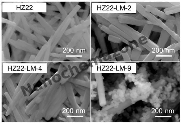
H-ZSM-22 (253853)

Price range: $350.00 through $3,265.00
Select options This product has multiple variants. The options may be chosen on the product page
H-ZSM-22 (253853)

Pore Structure  TON Pore Size(nm)  0.55 - 0.80  SiO2/Al2O3  40 - 80, 80 - 150, 150 - 300 Relative Crystallinity(%)   >= 95 Na2O weight(%)  <= 0.1 Loss on Ignition(%)  <= 5 

 
Product Codes- NCZ-2726K

Tungsten (W) Sputtering Targets, Purity: 99.95%, Size: 3”, Thickness: 0.250”

$351.00

Product 

Tungsten (W) Sputtering Targets, Purity: 99.95%, Size: 3'', Thickness: 0.250''

CAS No.

7440-33-7

Appearance

Powder

Purity

≥99%,  ≥99.9%,  ≥95%

(Other purities are also available)

APS

N/A  (Size Can be customized), Ask for other available size ranges.

Ingredient

N/A

Molecular Weight

 183.84 g/mol

Melting Point

3422 °C

Boiling Point

 5555 °C

Density

19.25 g/cm³

Product Codes

NCZ-1590K

Carbon (C) (Pyrolytic Graphite) Sputtering Targets, Purity: 99.999%, Size: 2”, Thickness: 0.125”

$351.00

Product 

Carbon (C) (Pyrolytic Graphite) Sputtering Targets, Purity: 99.999%, Size: 2'', Thickness: 0.125''

CAS No.

 7782-42-5

Appearance

Powder

Purity

≥99%,  ≥99.9%,  ≥95%

(Other purities are also available)

APS

 N/A (Size Can be customized), Ask for other available size ranges.

Ingredient

N/A

Molecular Weight

 12.01 g/mol

Melting Point

Sublimes ~3652 °C (no true melting)

Boiling Point

Sublimes directly ~4,200°C

Density

 ~2.2–2.25 g/cm³

Product Codes

NCZ-2342K

Antimony (Sb) Sputtering Targets, Purity: 99.999%, Size: 2”, Thickness: 0.125”

$351.00

Product 

Antimony (Sb) Sputtering Targets, Purity: 99.999%, Size: 2'', Thickness: 0.125''

CAS No.

 7440-36-0

Appearance

Powder

Purity

≥99%,  ≥99.9%,  ≥95%

(Other purities are also available)

APS

N/A (Size Can be customized), Ask for other available size ranges.

Ingredient

N/A

Molecular Weight

 121.76 g/mol

Melting Point

 630.6 °C

Boiling Point

 1587 °C

Density

 6.69 g/cm³

Product Codes

NCZ-2508K

Carbon (C) (Pyrolytic Graphite) Sputtering Targets, Purity: 99.999%, Size: 3”, Thickness: 0.125”

$352.00

Applications of Sputtering Targets;

Film deposition is accomplished using sputtering targets. A technique for sputtering thin films is called "deposition made by sputter targets," which entails eroding material from a "target" source onto a "substrate" like a silicon wafer. Etching of the target is done using semiconductor sputtering targets. When selectivity is not an issue and a high degree of etching anisotropy is required, sputter etching is the method of choice. By removing the target material through etching, sputter targets are also utilized for investigation. In secondary ion spectroscopy (SIMS), one example is when the target material is sputtered at a steady pace. Mass spectrometry is used to quantify the concentration and identity of spewed atoms as the target is sputtered.

The target material's composition may be ascertained and even very low concentrations of contaminants can be found with the aid of the sputtering target.

There is also an application area for sputtering targets in space. One type of space weathering that alters the chemical and physical characteristics of airless worlds like the Moon and asteroids is sputtering.

3N (99.9%) Gadolinium (Gd) Pieces Evaporation Materials

Price range: $352.00 through $1,507.00
Select options This product has multiple variants. The options may be chosen on the product page
Product 3N (99.9%) Gadolinium (Gd) Pieces Evaporation Materials
CAS No. N/A
Appearance Grayish White, Semi-Metallic
Purity ≥99%,  ≥99.9%,  ≥95%(Other purities are also available)
APS N/A.
Ingredient Ge
Molecular Weight N/A
Melting Point 937 °C
Boiling Point N/A
Density N/A
Product Codes NCZ-148E

3N (99.9%) Yttrium Fluoride (YF3) Pieces (3-12mm) Evaporation Materials

Price range: $352.00 through $583.00
Select options This product has multiple variants. The options may be chosen on the product page
Product 3N (99.9%) Yttrium Fluoride (YF3) Pieces (3-12mm) Evaporation Materials
CAS No. 13709-49-4
Appearance White, Solid
Purity ≥99%,  ≥99.9%,  ≥95%(Other purities are also available)
APS 3-12mm (Size Can be customized),  Ask for other available size range.
Ingredient YF3
Molecular Weight 145.90 g/mol
Melting Point 1,387 °C
Boiling Point N/A
Density 4.01 g/cm3
Product Codes NCZ-166E

Aluminum Oxide (Al2O3) Sputtering Targets, Purity: 99.99%, Size: 2”, Thickness: 0.125”

$354.00

 Applications of Sputtering Targets;

Film deposition is accomplished using sputtering targets. A technique for sputtering thin films is called "deposition made by sputter targets," which entails eroding material from a "target" source onto a "substrate" like a silicon wafer. Etching of the target is done using semiconductor sputtering targets. When selectivity is not an issue and a high degree of etching anisotropy is required, sputter etching is the method of choice. By removing the target material through etching, sputter targets are also utilized for investigation. In secondary ion spectroscopy (SIMS), one example is when the target material is sputtered at a steady pace. Mass spectrometry is used to quantify the concentration and identity of spewed atoms as the target is sputtered. With the sputtering target's assistance, the

It is possible to identify the target material and even detect incredibly tiny impurity amounts.

There is also an application area for sputtering targets in space. One type of space weathering that alters the chemical and physical characteristics of airless worlds like the Moon and asteroids is sputtering.

With the chemical formula Al2O3, aluminum oxide is a compound made of aluminum and oxygen. Because of its high melting point, Al2O3 is useful as a refractory material and as an abrasive due to its hardness, as well as for the production of aluminum metal. Because of their superior properties, aluminum oxide thin films, which can be produced via aluminum oxide sputtering targets, are extensively employed in several mechanical, optical, and microelectronic applications.

Boron Nitride (BN) Sputtering Targets, Purity: 99.5%, Size: 1”, Thickness: 0.250”

$354.00

Applications of Sputtering Targets;

Film deposition is accomplished using sputtering targets. A technique for sputtering thin films is called "deposition made by sputter targets," which entails eroding material from a "target" source onto a "substrate" like a silicon wafer. Etching of the target is done using semiconductor sputtering targets. When selectivity is not an issue and a high degree of etching anisotropy is required, sputter etching is the method of choice. By removing the target material through etching, sputter targets are also utilized for investigation. In secondary ion spectroscopy (SIMS), one example is when the target material is sputtered at a steady pace. Mass spectrometry is used to quantify the concentration and identity of spewed atoms as the target is sputtered.

The target material's composition may be ascertained and even very low concentrations of contaminants can be found with the aid of the sputtering target.

There is also an application area for sputtering targets in space. One type of space weathering that alters the chemical and physical characteristics of airless worlds like the Moon and asteroids is sputtering.

Carbon (C) Sputtering Targets, indium, Purity: 99.999%, Size: 2”, Thickness: 0.125”

$355.00

Applications of Sputtering Targets;

Film deposition is accomplished using sputtering targets. A technique for sputtering thin films is called "deposition made by sputter targets," which entails eroding material from a "target" source onto a "substrate" like a silicon wafer. Etching of the target is done using semiconductor sputtering targets. When selectivity is not an issue and a high degree of etching anisotropy is required, sputter etching is the method of choice. By removing the target material through etching, sputter targets are also utilized for investigation. In secondary ion spectroscopy (SIMS), one example is when the target material is sputtered at a steady pace. Mass spectrometry is used to quantify the concentration and identity of spewed atoms as the target is sputtered.

The target material's composition may be ascertained and even very low concentrations of contaminants can be found with the aid of the sputtering target.

There is also an application area for sputtering targets in space. One type of space weathering that alters the chemical and physical characteristics of airless worlds like the Moon and asteroids is sputtering.

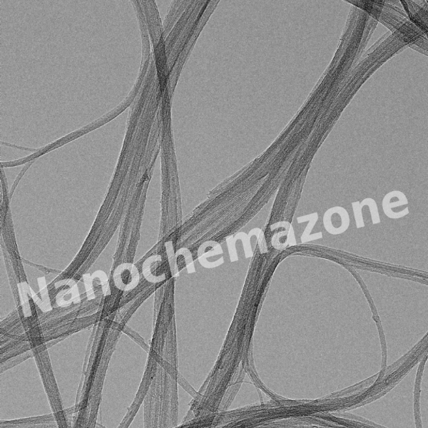
Silver nanowires/ Ag Nanowires

$355.00
$355/1g immersed in 25ml ethanol

Product 

Silver nanowires/ Ag Nanowires

CAS No.

7440-22-4

Appearance

Liquid

Purity

≥99%,  ≥99.9%,  ≥95%

(Other purities are also available)

APS

40+/- 10 nm (Size Can be customized), Ask for other available size ranges.

Ingredient

AlN

Molecular Weight

40.982 g/mol

Melting Point

2200 °C

Boiling Point

2517 °C

Density

3.3 g/cm³

Product Codes

NCZ-1009K

99.995% 4N5 Indium Foil (100x100x0.1 mm) for Heat Sink and Solid State Battery

$355.00
Select options This product has multiple variants. The options may be chosen on the product page
Product 99.995% 4N5 Indium Foil (100x100x0.1 mm) for Heat Sink and Solid State Battery
CAS No. 7440-74-6
Appearance Silvery, shiny metal foil
Purity ≥99%,  ≥99.9%,  ≥95%(Other purities are also available)
APS 100nm (Size Can be customized),  Ask for other available size range.
Ingredient In
Molecular Weight 138.205 g/mol
Melting Point 156.6 °C
Boiling Point N/A
Density 7.31 g/cm³
Product Codes NCZ-253I

Silicon (Si) Sputtering Targets, P-type, Purity: 99.999%, Size: 4”, Thickness: 0.125”

$355.00

Product 

Silicon (Si) Sputtering Targets, P-type, Purity: 99.999%, Size: 4'', Thickness: 0.125''

CAS No.

7440-21-3

Appearance

Powder

Purity

≥99%,  ≥99.9%,  ≥95%

(Other purities are also available)

APS

N/A  (Size Can be customized), Ask for other available size ranges.

Ingredient

N/A

Molecular Weight

28.0855 g/mol

Melting Point

 1,414 °C

Boiling Point

3,265 °C

Density

 2.33 g/cm³

Product Codes

NCZ-1747K

Aluminum Laminated Film for Pouch Cell Case

Price range: $357.00 through $1,095.00
Select options This product has multiple variants. The options may be chosen on the product page

Applications:

Aluminum Laminated Film for Pouch Cell Case is used as casing material for polymer Li-Ion battery.

Fullerene-C70, Purity: 99.5%

Price range: $357.00 through $1,675.00
Select options This product has multiple variants. The options may be chosen on the product page

Applications:

1. Pharmaceutical: Diagnostic reagents, super drugs, cosmetics, nuclear magnetic resonance (NMR) with the developer. DNA affinity 2. Energy: Solar battery, fuel cell, secondary battery. 3. Industry: Wear resistant material, flame retardant materials, lubricants, polymer additives, high-performance membrane, catalyst, artificial diamond, hard alloy, electric viscous fluid, ink filters, high-performance coatings, fire retardant coatings, manufacturing bioactive materials , memory materials, embedded molecular and other characteristics, composite materials etc. 4. Information industry: Semiconductor record medium, magnetic materials, printing ink, toner, ink, paper special purposes. 5. Electronic parts: Superconducting semiconductor, diodes, transistors, inductor.  , 6. Optical materials, electronic camera, fluorescence display tube, nonlinear optical materials. 7. Environment: Gas adsorption, gas storage.

Indium Zinc Oxide/IZO (InZnO) Sputtering Targets, Purity: 99.99%, Size: 2”, Thickness: 0.125”

$357.00

Applications of Sputtering Targets;

Film deposition is accomplished using sputtering targets. A technique for sputtering thin films is called "deposition made by sputter targets," which entails eroding material from a "target" source onto a "substrate" like a silicon wafer. Etching of the target is done using semiconductor sputtering targets. When selectivity is not an issue and a high degree of etching anisotropy is required, sputter etching is the method of choice. By removing the target material through etching, sputter targets are also utilized for investigation. In secondary ion spectroscopy (SIMS), one example is when the target material is sputtered at a steady pace. Mass spectrometry is used to quantify the concentration and identity of spewed atoms as the target is sputtered.

The target material's composition may be ascertained and even very low concentrations of contaminants can be found with the aid of the sputtering target.

There is also an application area for sputtering targets in space. One type of space weathering that alters the chemical and physical characteristics of airless worlds like the Moon and asteroids is sputtering.

Nickel Vanadium (NiV) Sputtering Targets, Purity: 99.95%, Size: 4”, Thickness: 0.125”

$357.00

Applications of Sputtering Targets;

Film deposition is accomplished using sputtering targets. A technique for sputtering thin films is called "deposition made by sputter targets," which entails eroding material from a "target" source onto a "substrate" like a silicon wafer. Etching of the target is done using semiconductor sputtering targets. When selectivity is not an issue and a high degree of etching anisotropy is required, sputter etching is the method of choice. By removing the target material through etching, sputter targets are also utilized for investigation. In secondary ion spectroscopy (SIMS), one example is when the target material is sputtered at a steady pace. Mass spectrometry is used to quantify the concentration and identity of spewed atoms as the target is sputtered.

The target material's composition may be ascertained and even very low concentrations of contaminants can be found with the aid of the sputtering target.

There is also an application area for sputtering targets in space. One type of space weathering that alters the chemical and physical characteristics of airless worlds like the Moon and asteroids is sputtering.

Silicon (Si) Sputtering Targets, P-type, Purity: 99.999%, Size: 4”, Thickness: 0.250”

$357.00

Applications of Sputtering Targets;

Film deposition is accomplished using sputtering targets. A technique for sputtering thin films is called "deposition made by sputter targets," which entails eroding material from a "target" source onto a "substrate" like a silicon wafer. Etching of the target is done using semiconductor sputtering targets. When selectivity is not an issue and a high degree of etching anisotropy is required, sputter etching is the method of choice. By removing the target material through etching, sputter targets are also utilized for investigation. In secondary ion spectroscopy (SIMS), one example is when the target material is sputtered at a steady pace. Mass spectrometry is used to quantify the concentration and identity of spewed atoms as the target is sputtered.

The target material's composition may be ascertained and even very low concentrations of contaminants can be found with the aid of the sputtering target.

There is also an application area for sputtering targets in space. One type of space weathering that alters the chemical and physical characteristics of airless worlds like the Moon and asteroids is sputtering.

Tungsten Titanium (TiW) Sputtering Targets, Purity: 99.99%, Size: 4”, Thickness: 0.250”

$357.00

Applications of Sputtering Targets;

Film deposition is accomplished using sputtering targets. A technique for sputtering thin films is called "deposition made by sputter targets," which entails eroding material from a "target" source onto a "substrate" like a silicon wafer. Etching of the target is done using semiconductor sputtering targets. When selectivity is not an issue and a high degree of etching anisotropy is required, sputter etching is the method of choice. By removing the target material through etching, sputter targets are also utilized for investigation. In secondary ion spectroscopy (SIMS), one example is when the target material is sputtered at a steady pace. Mass spectrometry is used to quantify the concentration and identity of spewed atoms as the target is sputtered.

The target material's composition may be ascertained and even very low concentrations of contaminants can be found with the aid of the sputtering target.

There is also an application area for sputtering targets in space. One type of space weathering that alters the chemical and physical characteristics of airless worlds like the Moon and asteroids is sputtering.

Nickel Oxide (NiO) Sputtering Target

Price range: $357.00 through $990.00
Select options This product has multiple variants. The options may be chosen on the product page

Product 

Nickel Oxide (NiO) Sputtering Target

CAS No.

1313-99-1

Appearance

Powder

Purity

≥99%,  ≥99.9%,  ≥95%

(Other purities are also available)

APS

 NA (Size Can be customized), Ask for other available size ranges.

Ingredient

N/A

Molecular Weight

74.69 g/mol

Melting Point

~1,950 °C

Boiling Point

~2,730 °C

Density

~6.67 g/cm³

Product Codes

NCZ-1321K

PTFE Separator Film for Battery Applications Thickness: 50μm, Width: 60mm, Length: 600 m, 1 roll: 600 m

Price range: $358.00 through $1,238.00
Select options This product has multiple variants. The options may be chosen on the product page
Product Information Product Name PTFE Separator Film for Battery Applications Thickness 50μm Width 60mm±0.005 Length 600m Product No NG10BEW0942 Elongation

Boron (B) Sputtering Targets, Purity: 99.9%, Size: 3”, Thickness: 0.125”

$358.00

Applications of Sputtering Targets;

Film deposition is accomplished using sputtering targets. A technique for sputtering thin films is called "deposition made by sputter targets," which entails eroding material from a "target" source onto a "substrate" like a silicon wafer. Etching of the target is done using semiconductor sputtering targets. When selectivity is not an issue and a high degree of etching anisotropy is required, sputter etching is the method of choice. By removing the target material through etching, sputter targets are also utilized for investigation. In secondary ion spectroscopy (SIMS), one example is when the target material is sputtered at a steady pace. Mass spectrometry is used to quantify the concentration and identity of spewed atoms as the target is sputtered.

The target material's composition may be ascertained and even very low concentrations of contaminants can be found with the aid of the sputtering target.

There is also an application area for sputtering targets in space. One type of space weathering that alters the chemical and physical characteristics of airless worlds like the Moon and asteroids is sputtering.

Germanium (Ge) Sputtering Targets, Purity: 99.999%, Size: 2”, Thickness: 0.250”

$358.00

Product 

Germanium (Ge) Sputtering Targets, Purity: 99.999%, Size: 2'', Thickness: 0.250''

CAS No.

7440-56-4

Appearance

Powder

Purity

≥99%,  ≥99.9%,  ≥95%

(Other purities are also available)

APS

 N/A (Size Can be customized), Ask for other available size ranges.

Ingredient

N/A

Molecular Weight

 72.63 g/mol

Melting Point

 938.3 °C

Boiling Point

2,833 °C

Density

 5.32 g/cm³

Product Codes

NCZ-2241K

High Purity (>95 wt%) Single-walled Carboxylated Carbon Nanotubes, 1g

$359.00
Product High Purity (>95 wt%) Single-walled Carboxylated Carbon Nanotubes, 1g
CAS No. 308068-56-6
Appearance Black 
Purity ≥99%,  ≥99.9%,  ≥95%(Other purities are also available)
APS 1–2 nm (Size Can be customized),  Ask for other available size range.
Ingredient (C)x(COOH)y
Molecular Weight N/A
Melting Point N/A
Boiling Point N/A
Density 1.3–1.4 g/cm³
Product Codes NCZ-388I

Aluminum Nickel Composite Strip for Battery Tab, Width: 4 mm, Thickness: 0.1 mm, 1Roll: 1 kg

Price range: $360.00 through $1,225.00
Select options This product has multiple variants. The options may be chosen on the product page

Applications:

Aluminum Nickel Composite Strip for Battery Tab is mainly used for welding aluminum casing parts of lithium ion batteries.

Silicon (Si) Sputtering Targets, undoped, Purity: 99.999%, Size: 4”, Thickness: 0.125”

$360.00

Applications of Sputtering Targets;

Film deposition is accomplished using sputtering targets. A technique for sputtering thin films is called "deposition made by sputter targets," which entails eroding material from a "target" source onto a "substrate" like a silicon wafer. Etching of the target is done using semiconductor sputtering targets. When selectivity is not an issue and a high degree of etching anisotropy is required, sputter etching is the method of choice. By removing the target material through etching, sputter targets are also utilized for investigation. In secondary ion spectroscopy (SIMS), one example is when the target material is sputtered at a steady pace. Mass spectrometry is used to quantify the concentration and identity of spewed atoms as the target is sputtered.

The target material's composition may be ascertained and even very low concentrations of contaminants can be found with the aid of the sputtering target.

There is also an application area for sputtering targets in space. One type of space weathering that alters the chemical and physical characteristics of airless worlds like the Moon and asteroids is sputtering.

99.9999% 6N Gallium (Ga) Metal

$362.00
Select options This product has multiple variants. The options may be chosen on the product page
Product 99.9999% 6N Gallium (Ga) Metal
CAS No. 7440-55-3
Appearance Silvery-white, soft metal
Purity ≥99%,  ≥99.9%,  ≥95%(Other purities are also available)
APS 1–10mm (Size Can be customized),  Ask for other available size range.
Ingredient Ga
Molecular Weight 69.72 g/mol
Melting Point 29.76 °C
Boiling Point N/A
Density 5.904 g/cm³
Product Codes NCZ-266I

Selenium (Se) Sputtering Targets, elastomer, Purity: 99.999%, Size: 2”, Thickness: 0.125”

$362.00

Product 

Selenium (Se) Sputtering Targets, elastomer, Purity: 99.999%, Size: 2'', Thickness: 0.125''

CAS No.

7782-49-2

Appearance

Powder

Purity

≥99%,  ≥99.9%,  ≥95%

(Other purities are also available)

APS

N/A  (Size Can be customized), Ask for other available size ranges.

Ingredient

N/A

Molecular Weight

 78.96 g/mol

Melting Point

 221 °C

Boiling Point

 685 °C

Density

 4.81 g/cm³

Product Codes

NCZ-1767K

Polyhydroxylated Fullerene (Fullerenols)/ C60, (-OH) Functionalized, Dispersed in Water, 2000 ppm Dry powder

Price range: $363.00 through $4,422.00
Select options This product has multiple variants. The options may be chosen on the product page
25 ml/325 € 100 ml/990 € 500 ml/2760 € 1000 ml/3950 € Please contact us for quotes on larger quantities.

Polyhydroxylated Fullerene (Fullerenols)/ C60

(-OH) Functionalized, Dispersed in Water, 2000 ppm, Dry powder

The starting material is >98% purity C60 fullerenes. C60 bearing over 40 hydroxyl groups that have higher water solubility (>50 mg/mL). These exist as monodisperse nanoparticles in water, and have a valiant polishing effect. They exhibit superior antioxidant and anti-inflammatory properties.

Applications:

1. Pharmaceutical: Diagnostic reagents, super drugs,   cosmetics, nuclear magnetic resonance (NMR) with the developer. DNA affinity, anti-HIV drugs, anti-cancer drugs, chemotherapy drugs, cosmetics additives and scientific research. 2. Energy: Solar battery, fuel cell, secondary battery. 3. Industry: Wear resistant material, flame retardant materials, lubricants, polymer additives, high-performance membrane, catalyst, artificial diamond, hard alloy, electric viscous fluid, ink filters, high-performance coatings, fire retardant coatings, manufacturing bioactive materials , memory materials, embedded molecular and other characteristics, composite materials etc. 4. Information industry: Semiconductor record medium, magnetic materials, printing ink, toner, ink, paper special purposes. 5. Electronic parts: Superconducting semiconductor, diodes, transistors, inductor.  , 6. Optical materials, electronic camera, fluorescence display tube, nonlinear optical materials. 7. Environment: Gas adsorption, gas storage.  

Li-Ion Battery Separator Film, Thickness: 25 μm, Width: 60 mm, Length: 500 m, 1 Roll: 500 m

Price range: $363.00 through $1,425.00
Select options This product has multiple variants. The options may be chosen on the product page

Applications:

Li-Ion Battery Separator Film can be used as li-ion battery separator in battery R&D. The need for electric energy storage systems are in increasing demand. Lithium-ion batteries represent the best option for many applications such as hybrid and electric vehicles which require high energy density, cycle durability and charge/discharge efficiency.

Li-Ion Battery Separator Film, Thickness: 25 μm, Width: 60 mm, Length: 500 m, 1 Roll: 500 m

Price range: $363.00 through $1,425.00
Select options This product has multiple variants. The options may be chosen on the product page

Applications:

Li-Ion Battery Separator Film can be used as li-ion battery separator in battery R&D. The need for electric energy storage systems are in increasing demand. Lithium-ion batteries represent the best option for many applications such as hybrid and electric vehicles which require high energy density, cycle durability and charge/discharge efficiency.

Lanthanum Calcium Manganate (La0.7Ca0.3MnO3) Sputtering Targets, Purity: 99.9%, Size: 3”, Thickness: 0.125”

$363.00
Select options This product has multiple variants. The options may be chosen on the product page

Applications of Sputtering Targets;

  • Sputtering targets is used for film deposition. The deposition made by sputter targets is a method of depositing thin films by sputtering that involves eroding material from a "target" source onto a "substrate" such as  a silicon wafer.
  • Semiconductor sputtering targets is used to etch the target. Sputter etching is chosen in cases where a high degree of etching anisotropy is needed and selectivity is not a concern.
  • Sputter targets is also used for analysis by etching away the target material.
One of the example occurs in secondary ion spectroscopy (SIMS), where the target sample is sputtered at a constant rate. As the target is sputtered, the concentration and identity of sputtered atoms are measured using mass spectrometry. By helping of the sputtering target, the composition of the target material can be determined and even extremely low concentrations of impurities are detected. Sputtering target has also application area in space. Sputtering is one of the forms of space weathering, a process that changes the physical and chemical properties of airless bodies, such as asteroids and the Moon.

Lanthanum Calcium Manganate (La0.7Ca0.3MnO3) Sputtering Targets, Purity: 99.9%, Size: 3”, Thickness: 0.125”

$363.00

Applications of Sputtering Targets;

Film deposition is accomplished using sputtering targets. A technique for sputtering thin films is called "deposition made by sputter targets," which entails eroding material from a "target" source onto a "substrate" like a silicon wafer. Etching of the target is done using semiconductor sputtering targets. When selectivity is not an issue and a high degree of etching anisotropy is required, sputter etching is the method of choice. By removing the target material through etching, sputter targets are also utilized for investigation. In secondary ion spectroscopy (SIMS), one example is when the target material is sputtered at a steady pace. Mass spectrometry is used to quantify the concentration and identity of spewed atoms as the target is sputtered.

The target material's composition may be ascertained and even very low concentrations of contaminants can be found with the aid of the sputtering target.

There is also an application area for sputtering targets in space. One type of space weathering that alters the chemical and physical characteristics of airless worlds like the Moon and asteroids is sputtering.

99.5% 10-20nm Gamma Iron Oxide Fe2 O3 Nanoparticles

Price range: $363.00 through $660.00
Select options This product has multiple variants. The options may be chosen on the product page
Product 99.5% 10-20nm Gamma Iron Oxide Fe2 O3 Nanoparticles
CAS No. 1309-37-1
Appearance Reddish brown
Purity ≥99%,  ≥99.9%,  ≥95%(Other purities are also available)
APS 10-20nm (Size Can be customized),  Ask for other available size range.
Ingredient Fe₂O₃
Molecular Weight 24.82 g/mol
Melting Point N/A
Boiling Point N/A
Density N/A
Product Codes NCZ-216I

99.5% 20-30nm Alpha Iron Oxide Fe2 O3 Nanoparticles

Price range: $363.00 through $660.00
Select options This product has multiple variants. The options may be chosen on the product page
Product 99.5% 20-30nm Alpha Iron Oxide Fe2 O3 Nanoparticles
CAS No. 1309-37-1
Appearance Reddish-brown
Purity ≥99%,  ≥99.9%,  ≥95%(Other purities are also available)
APS 20-30nm (Size Can be customized),  Ask for other available size range.
Ingredient Fe₂O₃
Molecular Weight 159.69 g/mol
Melting Point 1565 °C
Boiling Point N/A
Density 5.24 g/cm³
Product Codes NCZ-217I

99.5% 50-100nm Ferroferric Oxide Fe3O4 Nanoparticles

Price range: $363.00 through $660.00
Select options This product has multiple variants. The options may be chosen on the product page
Product 99.5% 50-100nm Ferroferric Oxide Fe3O4 Nanoparticles
CAS No. 1317-61-9
Appearance Black to brownish-black
Purity ≥99%,  ≥99.9%,  ≥95%(Other purities are also available)
APS 50-100nm (Size Can be customized),  Ask for other available size range.
Ingredient Fe3O4 
Molecular Weight 159.69 g/mol
Melting Point N/A
Boiling Point N/A
Density 5.2 g/cm³
Product Codes NCZ-218I
 

Lithium Titanate (Li2TiO3) Powder, 99% 2N

Price range: $364.00 through $1,232.00
Select options This product has multiple variants. The options may be chosen on the product page
Product Lithium Titanate (Li2TiO3) Powder, 99% 2N
CAS No. 12031-82-2
Appearance White to light gray fine
Purity ≥99%,  ≥99.9%,  ≥95%(Other purities are also available)
APS 100nm (Size Can be customized),  Ask for other available size range.
Ingredient Li2TiO3
Molecular Weight 109.75 g/mol
Melting Point 1,250 °C
Boiling Point N/A
Density 3.4 g/cm³
Product Codes NCZ-446I
 

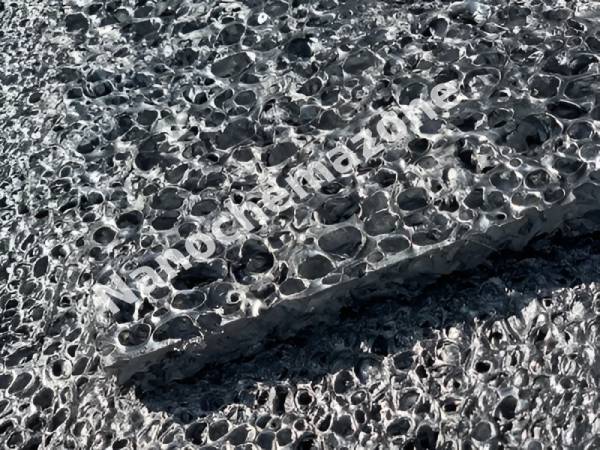
Aluminum Foam(Closed Macropore) (539569)

$364.00
Aluminum Foam(Closed Macropore) (539569)
Product # Density(g/cm³) Porosity(%) Primary pore diameter(mm)
539569-1 0.20-0.35 93-87 7-10
539569-2 0.36-0.50 87-81 5-7
539569-3 0.51-0.70 81-74 3-5
    Product Codes- NCZ-2668K

Trititanium pentoxide(Ti3O5, 99.99%) (221976)

$364.00
Select options This product has multiple variants. The options may be chosen on the product page
Trititanium pentoxide(Ti3O5, 99.99%) (221976)

Shape

Color

Purity

Package

Storage

Crystal

Granule

1-3 mm 3-5 mm

Purple black

99.99%

Avoid exposure to sunlight & acid Keep dry

Sinter

Tablet

9×5mm Upon demand

Tea black

 Granule

Upon demand

  Properties

CAS No.

Density (g/cm3)

Evaporation Temperature(°C)

Refractive Index at 550nm

Transparency Range(μm)

Evaporation Source

12065-65-5

4.89

1500~2000

2.2~2.3

0.4~8

RE, RS

Applications

AR coating; Beam Splitter; Cold light coating filter; HR coating; Glasses coating

Product Codes- NCZ-2786K