Chromium Oxide (Cr2O3) Sputtering Targets, Purity: 99.8%-99.9%, Size: 1”, Thickness: 0.125”

$294.00

Applications of Sputtering Targets;

Film deposition is accomplished using sputtering targets. A technique for sputtering thin films is called "deposition made by sputter targets," which entails eroding material from a "target" source onto a "substrate" like a silicon wafer. Etching of the target is done using semiconductor sputtering targets. When selectivity is not an issue and a high degree of etching anisotropy is required, sputter etching is the method of choice. By removing the target material through etching, sputter targets are also utilized for investigation. In secondary ion spectroscopy (SIMS), one example is when the target material is sputtered at a steady pace. Mass spectrometry is used to quantify the concentration and identity of spewed atoms as the target is sputtered.

The target material's composition may be ascertained and even very low concentrations of contaminants can be found with the aid of the sputtering target.

There is also an application area for sputtering targets in space. One type of space weathering that alters the chemical and physical characteristics of airless worlds like the Moon and asteroids is sputtering.

The inorganic chemical with the formula Cr2O3 is chromium oxide. Applications for chromium oxide sputtering targets are numerous. Let's examine a few instances where chromium oxide sputtering targets are employed instead. Low friction coefficients and high hardness values are displayed by Cr2O3 thin films. Because of these qualities, chromium oxide is a strong contender to take the place of Al2O3 or transition metal nitrides in certain applications.

Permalloy (Ni-Fe-Mo) Sputtering Targets, Size: 3”, Thickness: 0.250”

$294.00

Applications of Sputtering Targets;

Film deposition is accomplished using sputtering targets. A technique for sputtering thin films is called "deposition made by sputter targets," which entails eroding material from a "target" source onto a "substrate" like a silicon wafer. Etching of the target is done using semiconductor sputtering targets. When selectivity is not an issue and a high degree of etching anisotropy is required, sputter etching is the method of choice. By removing the target material through etching, sputter targets are also utilized for investigation. In secondary ion spectroscopy (SIMS), one example is when the target material is sputtered at a steady pace. Mass spectrometry is used to quantify the concentration and identity of spewed atoms as the target is sputtered.

The target material's composition may be ascertained and even very low concentrations of contaminants can be found with the aid of the sputtering target.

There is also an application area for sputtering targets in space. One type of space weathering that alters the chemical and physical characteristics of airless worlds like the Moon and asteroids is sputtering.

Zinc Oxide (ZnO) with Alumina Sputtering Targets, Purity: 99.99%, Size: 2”, Thickness: 0.125”

$294.00

Applications of Sputtering Targets;

Film deposition is accomplished using sputtering targets. A technique for sputtering thin films is called "deposition made by sputter targets," which entails eroding material from a "target" source onto a "substrate" like a silicon wafer. Etching of the target is done using semiconductor sputtering targets. When selectivity is not an issue and a high degree of etching anisotropy is required, sputter etching is the method of choice. By removing the target material through etching, sputter targets are also utilized for investigation. In secondary ion spectroscopy (SIMS), one example is when the target material is sputtered at a steady pace. Mass spectrometry is used to quantify the concentration and identity of spewed atoms as the target is sputtered.

The target material's composition may be ascertained and even very low concentrations of contaminants can be found with the aid of the sputtering target.

There is also an application area for sputtering targets in space. One type of space weathering that alters the chemical and physical characteristics of airless worlds like the Moon and asteroids is sputtering.

Zinc Oxide (ZnO) with Alumina Sputtering Targets, Purity: 99.99%, Size: 2”, Thickness: 0.125”

$294.00

Applications of Sputtering Targets;

Film deposition is accomplished using sputtering targets. A technique for sputtering thin films is called "deposition made by sputter targets," which entails eroding material from a "target" source onto a "substrate" like a silicon wafer. Etching of the target is done using semiconductor sputtering targets. When selectivity is not an issue and a high degree of etching anisotropy is required, sputter etching is the method of choice. By removing the target material through etching, sputter targets are also utilized for investigation. In secondary ion spectroscopy (SIMS), one example is when the target material is sputtered at a steady pace. Mass spectrometry is used to quantify the concentration and identity of spewed atoms as the target is sputtered.

The target material's composition may be ascertained and even very low concentrations of contaminants can be found with the aid of the sputtering target.

There is also an application area for sputtering targets in space. One type of space weathering that alters the chemical and physical characteristics of airless worlds like the Moon and asteroids is sputtering.

Silicon (Si) Sputtering Targets, P-type, Purity: 99.999%, Size: 2”, Thickness: 0.250”

$294.00

Product 

Silicon (Si) Sputtering Targets, P-type, Purity: 99.999%, Size: 2'', Thickness: 0.250''

CAS No.

7440-21-3

Appearance

Powder

Purity

≥99%,  ≥99.9%,  ≥95%

(Other purities are also available)

APS

N/A  (Size Can be customized), Ask for other available size ranges.

Ingredient

N/A

Molecular Weight

28.0855 g/mol

Melting Point

 1,414 °C

Boiling Point

3,265 °C

Density

 2.33 g/cm³

Product Codes

NCZ-1750K

Nickel Iron (Ni-Fe) Sputtering Targets, Purity: 99.5%, Size: 3”, Thickness: 0.125”

$294.00

Product 

Nickel Iron (Ni-Fe) Sputtering Targets, Purity: 99.5%, Size: 3'', Thickness: 0.125''

CAS No.

N/A

Appearance

Powder

Purity

≥99%,  ≥99.9%,  ≥95%

(Other purities are also available)

APS

 N/A (Size Can be customized), Ask for other available size ranges.

Ingredient

N/A

Molecular Weight

 ~57.5 g/mol

Melting Point

~1,430–1,480 °C

Boiling Point

N/A

Density

 ~8.1–8.7 g/cm³ (≈8.7 typical for ~80/20 alloy)

Product Codes

NCZ-1844K

Nickel Chromium (Ni-Cr) Sputtering Targets, Purity: 99.95%, Size: 3”, Thickness: 0.125”

$294.00

Product 

Nickel Chromium (Ni-Cr) Sputtering Targets, Purity: 99.95%, Size: 3'', Thickness: 0.125''

CAS No.

 11106-97-1

Appearance

Powder

Purity

≥99%,  ≥99.9%,  ≥95%

(Other purities are also available)

APS

 N/A (Size Can be customized), Ask for other available size ranges.

Ingredient

N/A

Molecular Weight

 ~110.69 g/mol

Melting Point

 ~1,400 °C

Boiling Point

 ~2,730–2,750 °C

Density

 ~8.4 – 8.5 g/cm³

Product Codes

NCZ-1856K

Aluminum Laminated Film, Width: 400 mm, Length: 7.5 m

Price range: $295.00 through $6,238.00
Select options This product has multiple variants. The options may be chosen on the product page

Applications:

Aluminum Laminated Film for Pouch Cell Case, 400 mm W x 7.5 m, L - EQ-alf-400-7.5M

Multi Walled Carbon Nanotubes Ethanol Dispersion, 3 wt%, Purity: > 95%, OD: 18-28 nm, Length: 8-28 µm

Price range: $295.00 through $1,425.00
Select options This product has multiple variants. The options may be chosen on the product page

Applications:

MWCNTs have numerous potential uses in various industries. Medical, mechanical, electric, chemical, energy, and other uses are among these. It can be used in the delivery of one medication, biosensors, CNT composites, catalysts, nanoprobes, hydrogen storage, nanomaterials for catalysis, eight gas discharge tubes, seven lithium batteries, nine-panel flat display, 11 transistors, 10 supercapacitors, twelve solar cells Photoluminescence 13 and template 14

Strong Graphene Aerogel, Diameter: 2±0.4 cm, Height: 2±0.4 cm

Price range: $295.00 through $1,185.00
Select options This product has multiple variants. The options may be chosen on the product page
1 piece/ 295 € 5 pieces/ 1185 € Contact us for tailored quotes on larger quantities & experience exceptional solutions from our

Aluminum Laminated Film, Width: 400 mm, Length: 7.5 m

Price range: $295.00 through $6,238.00
Select options This product has multiple variants. The options may be chosen on the product page

Molybdenum Disilicide (MoSi2) Sputtering Targets, Purity: 99.95%, Size: 1”, Thickness: 0.250”

$296.00

Applications of Sputtering Targets;

Film deposition is accomplished using sputtering targets. A technique for sputtering thin films is called "deposition made by sputter targets," which entails eroding material from a "target" source onto a "substrate" like a silicon wafer. Etching of the target is done using semiconductor sputtering targets. When selectivity is not an issue and a high degree of etching anisotropy is required, sputter etching is the method of choice. By removing the target material through etching, sputter targets are also utilized for investigation. In secondary ion spectroscopy (SIMS), one example is when the target material is sputtered at a steady pace. Mass spectrometry is used to quantify the concentration and identity of spewed atoms as the target is sputtered.

By helping of the sputtering target, the composition of the target material may be evaluated and even extremely tiny amounts of contaminants are recognized.

There is also an application area for sputtering targets in space. One type of space weathering that alters the chemical and physical characteristics of airless worlds like the Moon and asteroids is sputtering.

Zinc Sulfide (ZnS) Sputtering Targets, Purity: 99.99%, Size: 1”, Thickness: 0.250”

$296.00

Applications of Sputtering Targets;

Film deposition is accomplished using sputtering targets. A technique for sputtering thin films is called "deposition made by sputter targets," which entails eroding material from a "target" source onto a "substrate" like a silicon wafer. Etching of the target is done using semiconductor sputtering targets. When selectivity is not an issue and a high degree of etching anisotropy is required, sputter etching is the method of choice. By removing the target material through etching, sputter targets are also utilized for investigation. In secondary ion spectroscopy (SIMS), one example is when the target material is sputtered at a steady pace. Mass spectrometry is used to quantify the concentration and identity of spewed atoms as the target is sputtered.

The target material's composition may be ascertained and even very low concentrations of contaminants can be found with the aid of the sputtering target.

There is also an application area for sputtering targets in space. One type of space weathering that alters the chemical and physical characteristics of airless worlds like the Moon and asteroids is sputtering.

Multi Walled Carbon Nanotubes N-butanol Dispersion, 4 wt%, Purity: > 95%, OD: 8-16 nm, Length: 45 µm

Price range: $297.00 through $1,443.00
Select options This product has multiple variants. The options may be chosen on the product page

Applications:

MWCNTs are capable of being used in numerous industries. These applications span a variety of fields, including energy, mechanical, electrical, and chemical ones. One medicine delivery, for example, can use it. Biosensors, CNT composites, catalysis, nanoprobes, and hydrogen storage are among the other technologies. 8 gas discharge tubes, 7 lithium batteries, and 9-panel flat-panel display, supercapacitor ten, transistor eleven a dozen solar cells, 14-template, 13-photoluminescence

Silicon Carbide Wafer (SiC-4H) – 4H , Size: 2”, Thickness: 350 μm, Mechanical Grade, 4H Area: 80%

Price range: $297.00 through $1,302.00
Select options This product has multiple variants. The options may be chosen on the product page
Silicon Carbide Wafer (SiC-4H) – 4H Size: 2”, Thickness: 350 μm, 4H Area: 80% Technical Properties: Quality  Mechanical Grade Size (inch)  2”

Nickel Chromium (Ni-Cr) Sputtering Targets, Purity: 99.9%, Size: 3”, Thickness: 0.250”

$297.00

Applications of Sputtering Targets;

Film deposition is accomplished using sputtering targets. A technique for sputtering thin films is called "deposition made by sputter targets," which entails eroding material from a "target" source onto a "substrate" like a silicon wafer. Etching of the target is done using semiconductor sputtering targets. When selectivity is not an issue and a high degree of etching anisotropy is required, sputter etching is the method of choice. By removing the target material through etching, sputter targets are also utilized for investigation. In secondary ion spectroscopy (SIMS), one example is when the target mater

The target material's composition may be ascertained and even very low concentrations of contaminants can be found with the aid of the sputtering target.

There is also an application area for sputtering targets in space. One type of space weathering that alters the chemical and physical characteristics of airless worlds like the Moon and asteroids is sputtering.

ial is sputtered at a steady pace. Mass spectrometry is used to quantify the concentration and identity of spewed atoms as the target is sputtered.

Nickel Chromium (Ni-Cr) Sputtering Targets, Purity: 99.9%, Size: 4”, Thickness: 0.125”

$297.00

Applications of Sputtering Targets;

Film deposition is accomplished using sputtering targets. A technique for sputtering thin films is called "deposition made by sputter targets," which entails eroding material from a "target" source onto a "substrate" like a silicon wafer. Etching of the target is done using semiconductor sputtering targets. When selectivity is not an issue and a high degree of etching anisotropy is required, sputter etching is the method of choice. By removing the target material through etching, sputter targets are also utilized for investigation. In secondary ion spectroscopy (SIMS), one example is when the target material is sputtered at a steady pace. Mass spectrometry is used to quantify the concentration and identity of spewed atoms as the target is sputtered.

The target material's composition may be ascertained and even very low concentrations of contaminants can be found with the aid of the sputtering target.

There is also an application area for sputtering targets in space. One type of space weathering that alters the chemical and physical characteristics of airless worlds like the Moon and asteroids is sputtering.

99wt% Hollow Mesoporous Silica Powder

Price range: $297.00 through $550.00
Select options This product has multiple variants. The options may be chosen on the product page
Product 99wt% Hollow Mesoporous Silica Powder
CAS No. 7631-86-9
Appearance White or off-white fine
Purity ≥99%,  ≥99.9%,  ≥95%(Other purities are also available)
APS 100-500nm (Size Can be customized),  Ask for other available size range.
Ingredient SiO₂
Molecular Weight 60.08 g/mol
Melting Point N/A
Boiling Point N/A
Density 2.0–2.2 g/cm³
Product Codes NCZ-272I

High Purity (>95 wt%) Hydroxylate Single-walled Carbon Nanotube (Floating Catalyst Method), 1g

Price range: $297.00 through $469.00
Select options This product has multiple variants. The options may be chosen on the product page
Product High Purity (>95 wt%) Hydroxylate Single-walled Carbon Nanotube (Floating Catalyst Method), 1g
CAS No. N/A
Appearance Black to dark gray
Purity ≥99%,  ≥99.9%,  ≥95%(Other purities are also available)
APS N/A
Ingredient N/A
Molecular Weight N/A
Melting Point N/A
Boiling Point N/A
Density N/A
Product Codes NCZ-385I

Lithium Titanate (Li2TiO3) Sputtering Targets, Purity: 99.95%, Size: 2”, Thickness: 0.125”

$297.00

Product 

Lithium Titanate (Li2TiO3) Sputtering Targets, Purity: 99.95%, Size: 2'', Thickness: 0.125''

CAS No.

12031-82-2

Appearance

Powder

Purity

≥99%,  ≥99.9%,  ≥95%

(Other purities are also available)

APS

 N/A (Size Can be customized), Ask for other available size ranges.

Ingredient

N/A

Molecular Weight

109.75 g/mol

Melting Point

Decomposes before melting (~1,200 °C)

Boiling Point

N/A

Density

~3.41 g/cm³

Product Codes

NCZ-2013K

Samarium Chloride Hexahydrate (SmCl3 · 6H2O) 99.9% 3N

$297.00
Select options This product has multiple variants. The options may be chosen on the product page
Product Samarium Chloride Hexahydrate (SmCl3 · 6H2O) 99.9% 3N
CAS No. 13465-64-0
Appearance Light yellow to white crystalline
Purity ≥99%,  ≥99.9%,  ≥95%(Other purities are also available)
APS 100–500µm (Size Can be customized),  Ask for other available size range.
Ingredient SmCl3·6H2O
Molecular Weight 364.79 g/mol
Melting Point 2345 °C
Boiling Point N/A
Density 2.16 g/cm³
Product Codes NCZ-508I
 

Silver (Ag) Nanopowder/Nanoparticles Water Dispersion, Size: 15 nm, Tawny Color, 55.000 ppm

Price range: $298.00 through $3,720.00
Select options This product has multiple variants. The options may be chosen on the product page
Silver (Ag) Nanopowder/Nanoparticles Water Dispersion Size: 15 nm, Tawny Color, 55.000 ppm

Silver (Ag) Nanopowder/Nanoparticles Water Dispersion, Size: 15 nm, Tawny Color, 55.000 ppm

Price range: $298.00 through $3,720.00
Select options This product has multiple variants. The options may be chosen on the product page
25 mL/298 € 50 mL/435 € 100 mL/727 € 500 mL/2610 € 1000 mL/3720 €        Please contact us for quotes on larger

Magnesium (Mg) Micron Powder, Purity: 99.9%, Size: 0-300 µm

Price range: $298.00 through $4,825.00
Select options This product has multiple variants. The options may be chosen on the product page
1 kg/265 € 5 kg/1095 € 25 kg/4280 €                          Please contact us for quotes on larger quantities !!!

Magnesium (Mg) Micron Powder

Purity: 99.9%, Size: 0-300 µm

Technical Properties:

CAS Number 7439-95-4
Molecular Weight (g) 24.31
Average Particle Size (µm) 0-300
Apparent Density (g/cm3) 0.65 – 0.80
Appearance gray
Tmelting (oC) 650
Tboiling (oC) 1090
Electrical Resistivity (@ 20 °C) 4.45 microhm-cm
Thermal Conductivity (@ 298.2 K) 1.56 W/cm/K

Applications:

Magnesium is one of the lightest metals. This property gives Mg a wide range of applications from aircraft and automobile parts to material handling equipments, pyrotechnic, metallurgy, welding.  

Multi Walled Carbon Nanotubes Isopropanol Dispersion, 4 wt%, Purity: > 95%, OD: 18-35 nm, Length: 8-18 µm

Price range: $299.00 through $1,325.00
Select options This product has multiple variants. The options may be chosen on the product page

Applications:

MWCNTs have numerous potential uses in various industries. Midicine, mechanical, electric, chemical, energy, and other uses are among these. It can be used in a variety of applications, including medication delivery, biosensors, CNT composites, catalysis, nanoprobes, and hydrogen storage. seven lithium battalions tubes for 8 gas discharges, nine-panel flat display, 10-supercapacitor, 11-transistors, twelve solar cells Photoluminescence 13 and template 14

Multi Walled Carbon Nanotubes N-Methyl-2-Pyrrolidinone Dispersion, 4 wt%, Purity: > 96%, OD: 4-13 nm, Length: 45 µm

Price range: $299.00 through $1,200.00
Select options This product has multiple variants. The options may be chosen on the product page

Applications:

MWCNTs have numerous potential uses in various industries. Medical, mechanical, electric, chemical, energy, and other uses are among these. It can be used in the delivery of one medication, biosensors, CNT composites, catalysts, nanoprobes, hydrogen storage, nanomaterials for catalysis, eight gas discharge tubes, seven lithium batteries, nine-panel flat display, 11 transistors, 10 supercapacitors, twelve solar cells Photoluminescence 13 and template 14

Multi Walled Carbon Nanotubes Isopropanol Dispersion, 4wt%, Purity: > 96%, OD: 4-12 nm, Length: 55 µm

Price range: $299.00 through $1,285.00
Select options This product has multiple variants. The options may be chosen on the product page

Applications:

MWCNTs have numerous potential uses in various industries. Medical, mechanical, electric, chemical, energy, and other uses are among these. It can be used in the delivery of one medication, biosensors, CNT composites, catalysts, nanoprobes, hydrogen storage, nanomaterials for catalysis, eight gas discharge tubes, seven lithium batteries, nine-panel flat display, 11 transistors, 10 supercapacitors, twelve solar cells Photoluminescence 13 and template 14

Multi Walled Carbon Nanotubes Ethanol Dispersion, 4 wt%, Purity: > 96%, OD: 3-13 nm, Length: 45 µm

Price range: $299.00 through $1,365.00
Select options This product has multiple variants. The options may be chosen on the product page

Applications:

MWCNTs have numerous potential uses in various industries. Medical, mechanical, electric, chemical, energy, and other uses are among these. It can be used in the delivery of one medication, biosensors, CNT composites, catalysts, nanoprobes, hydrogen storage, nanomaterials for catalysis, eight gas discharge tubes, seven lithium batteries, nine-panel flat display, 11 transistors, 10 supercapacitors, twelve solar cells Photoluminescence 13 and template 14

Indium (In) Sputtering Targets, Purity: 99.99%, Size: 2”, Thickness: 0.250”

$299.00

Product 

Indium (In) Sputtering Targets, Purity: 99.99%, Size: 2'', Thickness: 0.250''

CAS No.

 7440-74-6

Appearance

Powder

Purity

≥99%,  ≥99.9%,  ≥95%

(Other purities are also available)

APS

 N/A (Size Can be customized), Ask for other available size ranges.

Ingredient

N/A

Molecular Weight

114.82 g/mol

Melting Point

 156.6 °C

Boiling Point

 2,072 °C

Density

 7.31 g/cm³

Product Codes

NCZ-2229K

Bismuth (Bi) Sputtering Targets, Purity: 99.999%, Size: 2”, Thickness: 0.250”

$299.00

Product 

Bismuth (Bi) Sputtering Targets, Purity: 99.999%, Size: 2'', Thickness: 0.250''

CAS No.

7440‑69‑9

Appearance

Powder

Purity

≥99%,  ≥99.9%,  ≥95%

(Other purities are also available)

APS

1 – 5 µm (Size Can be customized), Ask for other available size ranges.

Ingredient

N/A

Molecular Weight

~208.98 g/mol

Melting Point

 271.4 °C

Boiling Point

~1560 °C

Density

 ~9.78–9.80 g/cm³

Product Codes

NCZ-2437K

Aluminum (Al) Sputtering Targets, Purity: 99.999%, Size: 8”, Thickness: 0.250”

$299.00

Product 

Aluminum (Al) Sputtering Targets, Purity: 99.999%, Size: 8'', Thickness: 0.250''

CAS No.

 7429-90-5

Appearance

Powder

Purity

≥99%,  ≥99.9%,  ≥95%

(Other purities are also available)

APS

N/A (Size Can be customized), Ask for other available size ranges.

Ingredient

N/A

Molecular Weight

 26.98 g/mol

Melting Point

 660.3 °C

Boiling Point

 2519 °C

Density

 2.70 g/cm³

Product Codes

NCZ-2562K

Carbon Nanotube Fibres, Fiber diameter: 60-80 µm, Tensile Strength: 310-500 MPa, Electrical conductivity: 1×10^5~2×10^5 S/m

Price range: $300.00 through $1,127.00
Select options This product has multiple variants. The options may be chosen on the product page
Carbon Nanotube Fibres, Fiber diameter: 60-80 µm, Tensile Strength: 310-500 MPa, Electrical conductivity: 1×10⁵~2×10⁵ S/m Carbon nanotube fibers have moderate to

Impending Self-Help Transfer Nickel Graphene Foam, Thickness: 1±0.1 mm, Size: 2×2 cm

Price range: $300.00 through $1,389.00
Select options This product has multiple variants. The options may be chosen on the product page
Please contact us for quotes for larger quantities !   Impending self-help transfer nickel graphene foam is produced by etching the nickel of nickel graphene foam in etching liquid and being transferred to impending substrate. Graphene foam, can be gently released in deionized water and transferred directly to any base. This product is widely used for producing sensors, super capacitors and as the electrode materials of lithium battery to improve the battery capacity.

Bismuth Oxide (Bi2O3) Sputtering Targets, Purity: 99.9%, Size: 1”, Thickness: 0.250”

$300.00

Applications of Sputtering Targets;

Film deposition is accomplished using sputtering targets. A technique for sputtering thin films is called "deposition made by sputter targets," which entails eroding material from a "target" source onto a "substrate" like a silicon wafer. Etching of the target is done using semiconductor sputtering targets. When selectivity is not an issue and a high degree of etching anisotropy is required, sputter etching is the method of choice. By removing the target material through etching, sputter targets are also utilized for investigation. In secondary ion spectroscopy (SIMS), one example is when the target material is sputtered at a steady pace. Mass spectrometry is used to quantify the concentration and identity of spewed atoms as the target is sputtered.

The target material's composition may be ascertained and even very low concentrations of contaminants can be found with the aid of the sputtering target.

There is also an application area for sputtering targets in space. One type of space weathering that alters the chemical and physical characteristics of airless worlds like the Moon and asteroids is sputtering.

Indium Tin Oxide/ITO (In203:Sn02) Sputtering Targets, Purity: 99.99%, Size: 2”, Thickness: 0.125”

$300.00

Applications of Sputtering Targets;

Film deposition is accomplished using sputtering targets. A technique for sputtering thin films is called "deposition made by sputter targets," which entails eroding material from a "target" source onto a "substrate" like a silicon wafer. Etching of the target is done using semiconductor sputtering targets. When selectivity is not an issue and a high degree of etching anisotropy is required, sputter etching is the method of choice. By removing the target material through etching, sputter targets are also utilized for investigation. In secondary ion spectroscopy (SIMS), one example is when the target material is sputtered at a steady pace. Mass spectrometry is used to quantify the concentration and identity of spewed atoms as the target is sputtered.

The target material's composition may be ascertained and even very low concentrations of contaminants can be found with the aid of the sputtering target.

There is also an application area for sputtering targets in space. One type of space weathering that alters the chemical and physical characteristics of airless worlds like the Moon and asteroids is sputtering.

Molybdenum (Mo) Sputtering Targets, Purity: 99.95%, Size: 6”, Thickness: 0.125”

$300.00

Applications of Sputtering Targets;

Film deposition is accomplished using sputtering targets. A technique for sputtering thin films is called "deposition made by sputter targets," which entails eroding material from a "target" source onto a "substrate" like a silicon wafer. Etching of the target is done using semiconductor sputtering targets. When selectivity is not an issue and a high degree of etching anisotropy is required, sputter etching is the method of choice. By removing the target material through etching, sputter targets are also utilized for investigation. In secondary ion spectroscopy (SIMS), one example is when the target material is sputtered at a steady pace. Mass spectrometry is used to quantify the concentration and identity of spewed atoms as the target is sputtered.

By helping of the sputtering target, the composition of the target material may be evaluated and even extremely tiny amounts of contaminants are recognized.

There is also an application area for sputtering targets in space. One type of space weathering that alters the chemical and physical characteristics of airless worlds like the Moon and asteroids is sputtering.

Nickel (Ni) Sputtering Targets, Purity: 99.99%, Size: 6”, Thickness: 0.125”

$300.00

Applications of Sputtering Targets;

Film deposition is accomplished using sputtering targets. A technique for sputtering thin films is called "deposition made by sputter targets," which entails eroding material from a "target" source onto a "substrate" like a silicon wafer. Etching of the target is done using semiconductor sputtering targets. When selectivity is not an issue and a high degree of etching anisotropy is required, sputter etching is the method of choice. By removing the target material through etching, sputter targets are also utilized for investigation. In secondary ion spectroscopy (SIMS), one example is when the target material is sputtered at a steady pace. Mass spectrometry is used to quantify the concentration and identity of spewed atoms as the target is sputtered.

The target material's composition may be ascertained and even very low concentrations of contaminants can be found with the aid of the sputtering target.

There is also an application area for sputtering targets in space. One type of space weathering that alters the chemical and physical characteristics of airless worlds like the Moon and asteroids is sputtering.

Tin (Sn) Sputtering Targets, Purity: 99.99%, Size: 3”, Thickness: 0.250”

$301.00

Applications of Sputtering Targets;

Film deposition is accomplished using sputtering targets. A technique for sputtering thin films is called "deposition made by sputter targets," which entails eroding material from a "target" source onto a "substrate" like a silicon wafer. Etching of the target is done using semiconductor sputtering targets. When selectivity is not an issue and a high degree of etching anisotropy is required, sputter etching is the method of choice. By removing the target material through etching, sputter targets are also utilized for investigation. In secondary ion spectroscopy (SIMS), one example is when the target material is sputtered at a steady pace. Mass spectrometry is used to quantify the concentration and identity of spewed atoms as the target is sputtered.

The target material's composition may be ascertained and even very low concentrations of contaminants can be found with the aid of the sputtering target.

There is also an application area for sputtering targets in space. One type of space weathering that alters the chemical and physical characteristics of airless worlds like the Moon and asteroids is sputtering.

Zinc Oxide (ZnO) with Alumina Sputtering Targets, Purity: 99.95%, Size: 3”, Thickness: 0

$301.00

Applications of Sputtering Targets;

Film deposition is accomplished using sputtering targets. A technique for sputtering thin films is called "deposition made by sputter targets," which entails eroding material from a "target" source onto a "substrate" like a silicon wafer. Etching of the target is done using semiconductor sputtering targets. When selectivity is not an issue and a high degree of etching anisotropy is required, sputter etching is the method of choice. By removing the target material through etching, sputter targets are also utilized for investigation. In secondary ion spectroscopy (SIMS), one example is when the target material is sputtered at a steady pace. Mass spectrometry is used to quantify the concentration and identity of spewed atoms as the target is sputtered.

The target material's composition may be ascertained and even very low concentrations of contaminants can be found with the aid of the sputtering target.

There is also an application area for sputtering targets in space. One type of space weathering that alters the chemical and physical characteristics of airless worlds like the Moon and asteroids is sputtering.

Silicon (Si) Sputtering Targets, P-type, Purity: 99.999%, Size: 3”, Thickness: 0.125”

$301.00

Product 

Silicon (Si) Sputtering Targets, P-type, Purity: 99.999%, Size: 3'', Thickness: 0.125''

CAS No.

7440-21-3

Appearance

Powder

Purity

≥99%,  ≥99.9%,  ≥95%

(Other purities are also available)

APS

N/A  (Size Can be customized), Ask for other available size ranges.

Ingredient

N/A

Molecular Weight

28.0855 g/mol

Melting Point

 1,414 °C

Boiling Point

3,265 °C

Density

 2.33 g/cm³

Product Codes

NCZ-1749K

Aluminum (Al) Sputtering Targets, Purity: 99.999%, Size: 6”, Thickness: 0.125”

$301.00

Product 

Aluminum (Al) Sputtering Targets, Purity: 99.999%, Size: 6'', Thickness: 0.125''

CAS No.

 7429-90-5

Appearance

Powder

Purity

≥99%,  ≥99.9%,  ≥95%

(Other purities are also available)

APS

N/A (Size Can be customized), Ask for other available size ranges.

Ingredient

N/A

Molecular Weight

 26.98 g/mol

Melting Point

 660.3 °C

Boiling Point

 2519 °C

Density

 2.70 g/cm³

Product Codes

NCZ-2568K

Indium (In) Sputtering Targets, Purity: 99.999%, Size: 1”, Thickness: 0.250”

$302.00

Product 

Indium (In) Sputtering Targets, Purity: 99.999%, Size: 1'', Thickness: 0.250''

CAS No.

 7440-74-6

Appearance

Powder

Purity

≥99%,  ≥99.9%,  ≥95%

(Other purities are also available)

APS

 N/A (Size Can be customized), Ask for other available size ranges.

Ingredient

N/A

Molecular Weight

114.82 g/mol

Melting Point

 156.6 °C

Boiling Point

 2,072 °C

Density

 7.31 g/cm³

Product Codes

NCZ-2232K

CHOOSE OPTIONS COMPARE QUICK VIEW Lanthanum Strontium Manganate (La0.9Sr0.1MnO3) Sputtering Targets, Purity: 99.9%, Size: 1”, Thickness: 0.125”

$303.00
but allow experts a large degree of control over the growth and microstructure of the area.

Applications of Sputtering Targets;

  • Sputtering targets is used for film deposition. The deposition made by sputter targets is a method of depositing thin films by sputtering that involves eroding material from a "target" source onto a "substrate" such as  a silicon wafer.
  • Semiconductor sputtering targets is used to etch the target. Sputter etching is chosen in cases where a high degree of etching anisotropy is needed and selectivity is not a concern.
  • Sputter targets is also used for analysis by etching away the target material.
One of the example occurs in secondary ion spectroscopy (SIMS), where the target sample is sputtered at a constant rate. As the target is sputtered, the concentration and identity of sputtered atoms are measured using mass spectrometry. By helping of the sputtering target, the composition of the target material can be determined and even extremely low concentrations of impurities are detected. Sputtering target has also application area in space. Sputtering is one of the forms of space weathering, a process that changes the physical and chemical properties of airless bodies, such as asteroids and the Moon.

Bismuth Sputtering Target Bi

Price range: $303.00 through $604.00
Select options This product has multiple variants. The options may be chosen on the product page
Product Bismuth Sputtering Target Bi
CAS No. 7440-69-9
Appearance Solid, silvery-white to pinkish metallic luster
Purity ≥99%,  ≥99.9%,  ≥95%(Other purities are also available)
APS N/A
Ingredient Bi
Molecular Weight 208.98 g/mol
Melting Point N/A
Boiling Point N/A
Density 9.78 g/cm³
Product Codes NCZ-107H
 

Manganese Sputtering Target Mn

Price range: $303.00 through $1,025.00
Select options This product has multiple variants. The options may be chosen on the product page
Product Manganese Sputtering Target Mn
CAS No. N/A
Appearance Silvery Metallic
Purity ≥99%,  ≥99.9%,  ≥95%(Other purities are also available)
APS N/A
Ingredient Mn
Molecular Weight N/A
Melting Point 1,244 °C
Boiling Point N/A
Density 7.2 g/cm³
Product Codes NCZ-128H

Tungsten Titanium (TiW) Sputtering Targets, Purity: 99.99%, Size: 2”, Thickness: 0.125”

$303.00

Product 

Tungsten Titanium (TiW) Sputtering Targets, Purity: 99.99%, Size: 2'', Thickness: 0.125''

CAS No.

N/A

Appearance

Powder

Purity

≥99%,  ≥99.9%,  ≥95%

(Other purities are also available)

APS

N/A  (Size Can be customized), Ask for other available size ranges.

Ingredient

N/A

Molecular Weight

 170.5 g/mol

Melting Point

2,700 – 3,200 °C

Boiling Point

4,000 – 5,000 °C

Density

16.7 g/cm³

Product Codes

NCZ-1560K

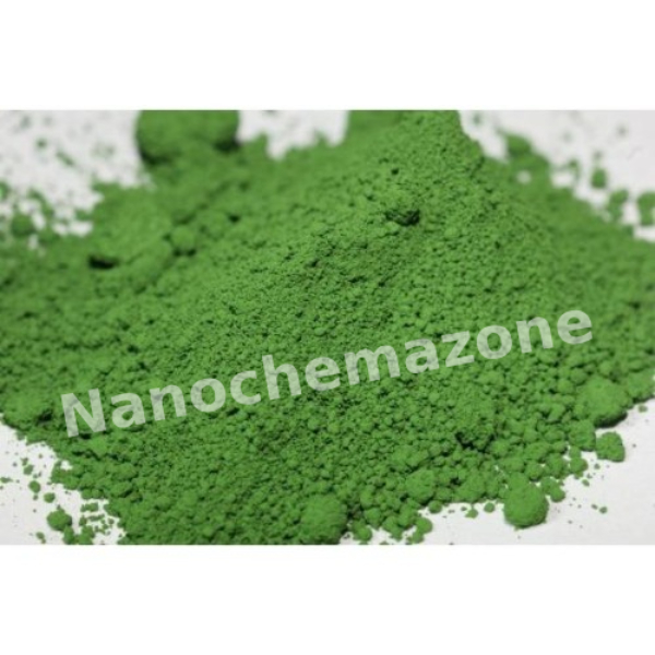
Chromium (III) Oxide (Cr2O3) Nanoparticles, 50nm, >99.9% Purity, 25g

$303.00
Product Chromium (III) Oxide (Cr2O3) Nanoparticles, 50nm, >99.9% Purity, 25g
CAS No. 1308-38-9
Appearance Green fine
Purity ≥99%,  ≥99.9%,  ≥95%(Other purities are also available)
APS 50nm (Size Can be customized),  Ask for other available size range.
Ingredient Cr2O3
Molecular Weight 151.99 g/mol
Melting Point N/A
Boiling Point N/A
Density 5.22 g/cm³
Product Codes NCZ-319I

Silicon Nitride (Si3N4) Sputtering Targets, Purity: 99.5%, Size: 1”, Thickness: 0.250”, Dark Gray to Black

$304.00

Product 

Silicon Nitride (Si3N4) Sputtering Targets, Purity: 99.5%, Size: 1'', Thickness: 0.250'', Dark Gray to Black

CAS No.

 12033-89-5

Appearance

Powder

Purity

≥99%,  ≥99.9%,  ≥95%

(Other purities are also available)

APS

N/A  (Size Can be customized), Ask for other available size ranges.

Ingredient

N/A

Molecular Weight

 140.28 g/mol

Melting Point

 ~1900 °C

Boiling Point

N/A

Density

~3.2 g/cm³

Product Codes

NCZ-1703K

Aluminum borate whisker(9Al2O3·2B2O3, D=0.3-2.0µm, L=15-60µm) (212675)

$304.00
Select options This product has multiple variants. The options may be chosen on the product page
Aluminum borate whisker(9Al2O3·2B2O3, D=0.3-2.0µm, L=15-60µm) (212675) Al2O3(Dry basis, %): 85±2.0 B2O3(Dry basis, %): 13±1.0 Length(μm): 10-60 Diameter(μm): 0.3-3.0 L/D Ratio: 20-80 Density(g/cm3): 2.93 pH: 6.5±0.5 Melting point(°C): 1440 Moisture(%): ≤0.5 Mohs hardness: 7
 
Product Codes- NCZ-2755K

Aluminum Oxide (Al2O3) Nanopowder/Nanoparticles Dispersion in 2-Propanol, Gamma, Size: 12 nm, 12 wt%

Price range: $305.00 through $1,553.00
Select options This product has multiple variants. The options may be chosen on the product page
Aluminum Oxide (Al2O3) Nanopowder/Nanoparticles Dispersion in 2-Propanol Gamma, Size: 12 nm, 12 wt%

Silicon Nanoparticles / Nanopowder ( Si, 98.5% 50 nm)

Price range: $305.00 through $725.00
Select options This product has multiple variants. The options may be chosen on the product page
$305/25g
$725/100g

Product 

Silicon Nanoparticles / Nanopowder ( Si, 98.5% 50 nm)

CAS No.

7440-21-3

Appearance

Powder

Purity

≥99%,  ≥99.9%,  ≥95%

(Other purities are also available)

APS

50 nm (Size Can be customized), Ask for other available size ranges.

Ingredient

N/A

Molecular Weight

28.0855 g/mol

Melting Point

1,414 °C

Boiling Point

3,265 °C

Density

~2.33 g/cm³

Product Codes

NCZ-1071K

Conductive Metal-Organic Framework (MOF) Ni3(HITP)2

$305.00
Product Conductive Metal-Organic Framework (MOF) Ni3(HITP)2
CAS No. N/A
Appearance Dark colored crystalline
Purity ≥99%,  ≥99.9%,  ≥95%(Other purities are also available)
APS 200–500nm (Size Can be customized),  Ask for other available size range.
Ingredient Ni₃(HITP)₂
Molecular Weight 666.9 g/mol
Melting Point N/A
Boiling Point N/A
Density N/A
Product Codes NCZ-323I

Silicon (Si) Sputtering Targets, P-type, Purity: 99.999%, Size: 3”, Thickness: 0.250”

$306.00

Product 

Silicon (Si) Sputtering Targets, P-type, Purity: 99.999%, Size: 3'', Thickness: 0.250''

CAS No.

7440-21-3

Appearance

Powder

Purity

≥99%,  ≥99.9%,  ≥95%

(Other purities are also available)

APS

N/A  (Size Can be customized), Ask for other available size ranges.

Ingredient

N/A

Molecular Weight

28.0855 g/mol

Melting Point

 1,414 °C

Boiling Point

3,265 °C

Density

 2.33 g/cm³

Product Codes

NCZ-1748K

Nickel Vanadium (NiV) Sputtering Targets, Purity: 99.95%, Size: 3”, Thickness: 0.125”

$306.00

Product 

Nickel Vanadium (NiV) Sputtering Targets, Purity: 99.95%, Size: 3'', Thickness: 0.125''

CAS No.

11137-91-4

Appearance

Powder

Purity

≥99%,  ≥99.9%,  ≥95%

(Other purities are also available)

APS

N/A (Size Can be customized), Ask for other available size ranges.

Ingredient

N/A

Molecular Weight

~57.9 g/mol

Melting Point

~1,350–1,450 °C

Boiling Point

N/A

Density

 ~8.5 g/cm³

Product Codes

NCZ-1826K

Indium Zinc Oxide/IZO (InZnO) Sputtering Targets, Purity: 99.99%, Size: 1”, Thickness: 0.250”

$306.00

Product 

Indium Zinc Oxide/IZO (InZnO) Sputtering Targets, Purity: 99.99%, Size: 1'', Thickness: 0.250''

CAS No.

Indium oxide (In₂O₃): 1312-43-2
Zinc oxide (ZnO): 1314-13-2

Appearance

Powder

Purity

≥99%,  ≥99.9%,  ≥95%

(Other purities are also available)

APS

 N/A (Size Can be customized), Ask for other available size ranges.

Ingredient

N/A

Molecular Weight

Approx. 260–270 g/mol (depends on ratio)

Melting Point

Indium oxide: ~1910 °C Zinc oxide: ~1975 °C

Boiling Point

N/A

Density

~7.1 g/cm³

Product Codes

NCZ-2200K

Hand-Held Disc Cutter with Ring Cutting Dies, ID: 8,15,18,20 mm

Price range: $307.00 through $1,532.00
Select options This product has multiple variants. The options may be chosen on the product page
 1 set: 307 Euro   5 set: 1532 Euro APPLICATIONS Hand-held disc cutter with 1 set of cutting dies, each set

Hand-Held Disc Cutter with Ring Cutting Dies, ID: 8,15,18,20 mm

Price range: $307.00 through $1,532.00
Select options This product has multiple variants. The options may be chosen on the product page
APPLICATIONS

Hand-held disc cutter with 1 set of cutting dies, each set includes 4 types of dies (ID: 8, 15, 18, 20 mm). It is a ideal and cost-effective tool for cutting battery separator. It is easy to change the cutter via a permanent magnet holder and good for operating in a glovebox.

Carbon (C) (Pyrolytic Graphite) Sputtering Targets, Purity: 99.999%, Size: 2”, Thickness: 0.125”

$307.00

Applications of Sputtering Targets;

Film deposition is accomplished using sputtering targets. A technique for sputtering thin films is called "deposition made by sputter targets," which entails eroding material from a "target" source onto a "substrate" like a silicon wafer. Etching of the target is done using semiconductor sputtering targets. When selectivity is not an issue and a high degree of etching anisotropy is required, sputter etching is the method of choice. By removing the target material through etching, sputter targets are also utilized for investigation. In secondary ion spectroscopy (SIMS), one example is when the target material is sputtered at a steady pace. Mass spectrometry is used to quantify the concentration and identity of spewed atoms as the target is sputtered.

The target material's composition may be ascertained and even very low concentrations of contaminants can be found with the aid of the sputtering target.

There is also an application area for sputtering targets in space. One type of space weathering that alters the chemical and physical characteristics of airless worlds like the Moon and asteroids is sputtering.

Magnesium Fluoride (MgF2) Sputtering Targets, Purity: 99.9%, Size: 1”, Thickness: 0.125”

$307.00

Applications of Sputtering Targets;

Film deposition is accomplished using sputtering targets. A technique for sputtering thin films is called "deposition made by sputter targets," which entails eroding material from a "target" source onto a "substrate" like a silicon wafer. Etching of the target is done using semiconductor sputtering targets. When selectivity is not an issue and a high degree of etching anisotropy is required, sputter etching is the method of choice. By removing the target material through etching, sputter targets are also utilized for investigation. In secondary ion spectroscopy (SIMS), one example is when the target material is sputtered at a steady pace. Mass spectrometry is used to quantify the concentration and identity of spewed atoms as the target is sputtered.

By helping of the sputtering target, the composition of the target material may be evaluated and even extremely tiny amounts of contaminants are recognized.

There is also an application area for sputtering targets in space. One type of space weathering that alters the chemical and physical characteristics of airless worlds like the Moon and asteroids is sputtering.

Manganese (Mn) Sputtering Targets, Purity: 99.95%, Size: 1”, Thickness: 0.250”

$307.00

Applications of Sputtering Targets;

Film deposition is accomplished using sputtering targets. A technique for sputtering thin films is called "deposition made by sputter targets," which entails eroding material from a "target" source onto a "substrate" like a silicon wafer. Etching of the target is done using semiconductor sputtering targets. When selectivity is not an issue and a high degree of etching anisotropy is required, sputter etching is the method of choice. By removing the target material through etching, sputter targets are also utilized for investigation. In secondary ion spectroscopy (SIMS), one example is when the target material is sputtered at a steady pace. Mass spectrometry is used to quantify the concentration and identity of spewed atoms as the target is sputtered.

By helping of the sputtering target, the composition of the target material may be evaluated and even extremely tiny amounts of contaminants are recognized.

There is also an application area for sputtering targets in space. One type of space weathering that alters the chemical and physical characteristics of airless worlds like the Moon and asteroids is sputtering.