Nickel Chromium (Ni-Cr) Sputtering Targets, Purity: 99.9%, Size: 2”, Thickness: 0.125”

$188.00

Applications of Sputtering Targets;

Film deposition is accomplished using sputtering targets. A technique for sputtering thin films is called "deposition made by sputter targets," which entails eroding material from a "target" source onto a "substrate" like a silicon wafer. Etching of the target is done using semiconductor sputtering targets. When selectivity is not an issue and a high degree of etching anisotropy is required, sputter etching is the method of choice. By removing the target material through etching, sputter targets are also utilized for investigation. In secondary ion spectroscopy (SIMS), one example is when the target material is sputtered at a steady pace. Mass spectrometry is used to quantify the concentration and identity of spewed atoms as the target is sputtered.

The target material's composition may be ascertained and even very low concentrations of contaminants can be found with the aid of the sputtering target.

There is also an application area for sputtering targets in space. One type of space weathering that alters the chemical and physical characteristics of airless worlds like the Moon and asteroids is sputtering.

Silicon Dioxide (SiO2) Sputtering Targets, Fused Quartz, Purity: 99.995%, Size: 4”, Thickness: 0.125”

$188.00

Applications of Sputtering Targets;

Film deposition is accomplished using sputtering targets. A technique for sputtering thin films is called "deposition made by sputter targets," which entails eroding material from a "target" source onto a "substrate" like a silicon wafer. Etching of the target is done using semiconductor sputtering targets. When selectivity is not an issue and a high degree of etching anisotropy is required, sputter etching is the method of choice. By removing the target material through etching, sputter targets are also utilized for investigation. In secondary ion spectroscopy (SIMS), one example is when the target material is sputtered at a steady pace. Mass spectrometry is used to quantify the concentration and identity of spewed atoms as the target is sputtered.

The target material's composition may be ascertained and even very low concentrations of contaminants can be found with the aid of the sputtering target.

There is also an application area for sputtering targets in space. One type of space weathering that alters the chemical and physical characteristics of airless worlds like the Moon and asteroids is sputtering.

Gallium Arsenide (GaAs) Wafers, Size: 4”, Thickness: 350±25 μm, Single Side Polished, EPI-ready

Price range: $189.00 through $3,588.00
Select options This product has multiple variants. The options may be chosen on the product page
Gallium Arsenide (GaAs) Wafer Size: 4”, Thickness: 350±25 μm, Single Side Polished Technical Properties: Quality  GaAs Materials  GaAs Size (inch)

Gallium Arsenide (GaAs) Wafers, Size: 2”, Thickness: 350±25 μm, Double Side Polished, EPI-ready

Price range: $189.00 through $3,588.00
Select options This product has multiple variants. The options may be chosen on the product page
Gallium Arsenide (GaAs) Wafer Size: 2”, Thickness: 350±25 μm, Double Side Polished Technical Properties: Quality  GaAs Materials  GaAs Size (inch)

Gallium Arsenide (GaAs) Wafers, Size: 2”, Thickness: 350±25 μm, Single Side Polished, EPI-ready, Mobility: 1000-3000

Price range: $189.00 through $3,588.00
Select options This product has multiple variants. The options may be chosen on the product page
Gallium Arsenide (GaAs) Wafer Size: 2”, Thickness: 350±25 μm, Mobility: 1000-3000 Technical Properties: Quality  GaAs Materials  GaAs Size (inch)  2” Thickness

Gallium Arsenide (GaAs) Wafers, Size: 2”, Thickness: 350± 25 μm, Orientation: 100, Single Side Polished, EPI-ready

Price range: $189.00 through $3,588.00
Select options This product has multiple variants. The options may be chosen on the product page
Gallium Arsenide (GaAs) Wafer Size: 2”, Thickness: 350±25 μm, Orientation: 100 Technical Properties: Quality  GaAs Materials  GaAs Size (inch)  2”

Erbium Oxide (Er2O3) Sputtering Targets, Purity: 99.99%, Size: 4”, Thickness: 0.250”

$189.00
Select options This product has multiple variants. The options may be chosen on the product page
 

Applications of Sputtering Targets;

  • Sputtering targets is used for film deposition. The deposition made by sputter targets is a method of depositing thin films by sputtering that involves eroding material from a "target" source onto a "substrate" such as  a silicon wafer.
  • Semiconductor sputtering targets is used to etch the target. Sputter etching is chosen in cases where a high degree of etching anisotropy is needed and selectivity is not a concern.
  • Sputter targets is also used for analysis by etching away the target material.
One of the example occurs in secondary ion spectroscopy (SIMS), where the target sample is sputtered at a constant rate. As the target is sputtered, the concentration and identity of sputtered atoms are measured using mass spectrometry. By helping of the sputtering target, the composition of the target material can be determined and even extremely low concentrations of impurities are detected. Sputtering target has also application area in space. Sputtering is one of the forms of space weathering, a process that changes the physical and chemical properties of airless bodies, such as asteroids and the Moon. Erbium oxide with a chemical formula of Er2Ois an oxide of erbium metal. The applications of erbium oxide are varied due to their electrical, optical and photoluminescence properties. Nanoscale materials doped with Er+3 are of much interest because they have special particle-size-dependent optical and electrical properties. Erbium oxide doped nanoparticle materials can be dispersed in glass or plastic for display purposes, such as display monitors. The spectroscopy of Er+3 electronic transitions in host crystals lattices of nanoparticles combined with ultrasonically formed geometries in aqueous solution of carbon nanotubes is of great interest for synthesis of photoluminescence nanoparticles in ‘green’ chemistry. Erbium oxide is among the most important rare earth metals used in biomedicine. Erbium oxides are also used as gate dielectrics in semiconductor devices since it has a high dielectric constant (10-14) and a large band gap. Erbium is sometimes used as a coloring for glasses and erbium oxide can also be used as a burnable neutron poison for nuclear fuel. Erbium oxide films obtained by sputtering can be used for their photoluminescence effect.

Erbium Oxide (Er2O3) Sputtering Targets, Purity: 99.99%, Size: 4”, Thickness: 0.250”

$189.00

Applications of Sputtering Targets;

Film deposition is accomplished using sputtering targets. A technique for sputtering thin films is called "deposition made by sputter targets," which entails eroding material from a "target" source onto a "substrate" like a silicon wafer. Etching of the target is done using semiconductor sputtering targets. When selectivity is not an issue and a high degree of etching anisotropy is required, sputter etching is the method of choice. By removing the target material through etching, sputter targets are also utilized for investigation. In secondary ion spectroscopy (SIMS), one example is when the target material is sputtered at a steady pace. Mass spectrometry is used to quantify the concentration and identity of spewed atoms as the target is sputtered.

The target material's composition may be ascertained and even very low concentrations of contaminants can be found with the aid of the sputtering target.

There is also an application area for sputtering targets in space. One type of space weathering that alters the chemical and physical characteristics of airless worlds like the Moon and asteroids is sputtering.

Nickel Vanadium (NiV) Sputtering Targets, Purity: 99.95%, Size: 1”, Thickness: 0.250”

$189.00

Applications of Sputtering Targets;

Film deposition is accomplished using sputtering targets. A technique for sputtering thin films is called "deposition made by sputter targets," which entails eroding material from a "target" source onto a "substrate" like a silicon wafer. Etching of the target is done using semiconductor sputtering targets. When selectivity is not an issue and a high degree of etching anisotropy is required, sputter etching is the method of choice. By removing the target material through etching, sputter targets are also utilized for investigation. In secondary ion spectroscopy (SIMS), one example is when the target material is sputtered at a steady pace. Mass spectrometry is used to quantify the concentration and identity of spewed atoms as the target is sputtered.

The target material's composition may be ascertained and even very low concentrations of contaminants can be found with the aid of the sputtering target.

There is also an application area for sputtering targets in space. One type of space weathering that alters the chemical and physical characteristics of airless worlds like the Moon and asteroids is sputtering.

Silicon (Si) Sputtering Targets, undoped, Purity: 99.999%, Size: 2”, Thickness: 0.250”

$189.00

Applications of Sputtering Targets;

Film deposition is accomplished using sputtering targets. A technique for sputtering thin films is called "deposition made by sputter targets," which entails eroding material from a "target" source onto a "substrate" like a silicon wafer. Etching of the target is done using semiconductor sputtering targets. When selectivity is not an issue and a high degree of etching anisotropy is required, sputter etching is the method of choice. By removing the target material through etching, sputter targets are also utilized for investigation. In secondary ion spectroscopy (SIMS), one example is when the target material is sputtered at a steady pace. Mass spectrometry is used to quantify the concentration and identity of spewed atoms as the target is sputtered.

The target material's composition may be ascertained and even very low concentrations of contaminants can be found with the aid of the sputtering target.

There is also an application area for sputtering targets in space. One type of space weathering that alters the chemical and physical characteristics of airless worlds like the Moon and asteroids is sputtering.

Zinc (Zn) Sputtering Targets, Purity: 99.95%, Size: 3”, Thickness: 0.250”

$189.00

Applications of Sputtering Targets;

Film deposition is accomplished using sputtering targets. A technique for sputtering thin films is called "deposition made by sputter targets," which entails eroding material from a "target" source onto a "substrate" like a silicon wafer. Etching of the target is done using semiconductor sputtering targets. When selectivity is not an issue and a high degree of etching anisotropy is required, sputter etching is the method of choice. By removing the target material through etching, sputter targets are also utilized for investigation. In secondary ion spectroscopy (SIMS), one example is when the target material is sputtered at a steady pace. Mass spectrometry is used to quantify the concentration and identity of spewed atoms as the target is sputtered.

The target material's composition may be ascertained and even very low concentrations of contaminants can be found with the aid of the sputtering target.

There is also an application area for sputtering targets in space. One type of space weathering that alters the chemical and physical characteristics of airless worlds like the Moon and asteroids is sputtering.

Zinc (Zn) Sputtering Targets, Purity: 99.99%, Size: 4”, Thickness: 0.125”

$189.00

Applications of Sputtering Targets;

Film deposition is accomplished using sputtering targets. A technique for sputtering thin films is called "deposition made by sputter targets," which entails eroding material from a "target" source onto a "substrate" like a silicon wafer. Etching of the target is done using semiconductor sputtering targets. When selectivity is not an issue and a high degree of etching anisotropy is required, sputter etching is the method of choice. By removing the target material through etching, sputter targets are also utilized for investigation. In secondary ion spectroscopy (SIMS), one example is when the target material is sputtered at a steady pace. Mass spectrometry is used to quantify the concentration and identity of spewed atoms as the target is sputtered.

The target material's composition may be ascertained and even very low concentrations of contaminants can be found with the aid of the sputtering target.

There is also an application area for sputtering targets in space. One type of space weathering that alters the chemical and physical characteristics of airless worlds like the Moon and asteroids is sputtering.

Silver (Ag) Sputtering Target

Price range: $189.00 through $684.00
Select options This product has multiple variants. The options may be chosen on the product page

Product 

Silver (Ag) Sputtering Target

CAS No.

7440-22-4

Appearance

Powder

Purity

≥99%,  ≥99.9%,  ≥95%

(Other purities are also available)

APS

 NA (Size Can be customized), Ask for other available size ranges.

Ingredient

N/A

Molecular Weight

107.8682 g/mol

Melting Point

 961.78 °C

Boiling Point

2,162 °C

Density

10.49 g/cm³

Product Codes

NCZ-1304K

Yttrium Sputtering Target Y

Price range: $189.00 through $967.00
Select options This product has multiple variants. The options may be chosen on the product page
Product Yttrium Sputtering Target Y
CAS No. 7440-65-5
Appearance Silvery White, Metallic
Purity ≥99%,  ≥99.9%,  ≥95% (Other purities are also available)
APS N/A
Ingredient Y
Molecular Weight 88.91 g/mol
Melting Point 1,522 °C
Boiling Point N/A
Density N/A
Product Codes NCZ-148H
 

Magnesium Fluoride, MgF2 99.99% 4N High Purity Powder

Price range: $189.00 through $489.00
Select options This product has multiple variants. The options may be chosen on the product page
Product Magnesium Fluoride, MgF2 99.99% 4N High Purity Powder
CAS No. 7783-40-6
Appearance White, odorless crystalline
Purity ≥99%,  ≥99.9%,  ≥95%(Other purities are also available)
APS 1-10nm (Size Can be customized),  Ask for other available size range.
Ingredient MgF2
Molecular Weight 62.30 g/mol
Melting Point 1,261 °C
Boiling Point 2,260 °C
Density 3.15 g/cm³
Product Codes NCZ-450I
 

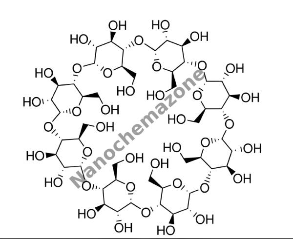
γ-Cyclodextrin (238605)

$189.00
Select options This product has multiple variants. The options may be chosen on the product page
γ-Cyclodextrin (238605)

Feature:

gamma-Cyclodextrin is a ring-shaped molecule made up of eight glucose units linked by alpha-1,4-bonds. The solubility degree of gamma-cyclodextrin in water is 23.2 g/100ml @ 25°C, which is higher than alpha-cyclodextrin and beta-cyclodextrin, and it is used to allow formation of inclusion complexes with bigger molecules.

CAS : 17465-86-0

Molecular Formula: C48H80O40

Molecular Weight: 1297.12

Specifications:  
Items Index
Appearance White powder, Odorless, Minor sweet
Assay ≥ 98.0%
Moisture content ≤11.0%
Residue on ignition ≤0.1%
Specific rotation +172°~+180°
Color and clarity of solution Clear and colorless
Reductive sugar ≤0.2%
Chloride ≤0.018%
Heavy metal ≤0.0002%
As ≤0.00013%
Total bacteria count ≤1000pcs/g
Moulds and yeasts ≤200pcs/g
Escherichia coli Negative
Product Codes- NCZ-2762K

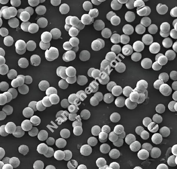
Mesocarbon Microbeads (MCMB) Graphite Micron Powder for Lithium Ion Battery

Price range: $190.00 through $334.00
Select options This product has multiple variants. The options may be chosen on the product page
500 grams/168 € 1000 grams/295 €
Please contact us for quotes on larger quantities !!!

Mesocarbon Microbeads (MCMB) Graphite Micron Powder for Lithium Ion Battery

SSA: 1.539 m2/g, Black Powder

MCMB (mesocarbon microbeads) synthetic graphite is prepared from petroleum pitch or coal tar. MCMB is one of the promising carbon anode materials for Li-ion batteries. MCMB has high specific capacity and a spherical structure, which is benefitial for high packing density of the anode. The low surface area of MCMB can minimize the unfavorable side reactions during the charge-discharge process. We offer Mesocarbon Microbeads(MCMB) Graphite Micron Powder for Lithium Ion Battery with low prices.

Technical Properties:

Appearance of MCMB Black Powder
Linear Formula C
CAS Number of MCMB 7782-42-5
Packed Container sealed in Al vacuumed bag
 
 D10  µm  7.195
 D50  µm  11.440
 D90  µm  18.000
 Moisture  %  0.025
 Tap  G/cm3  1.215
 SSA  M2/g  1.539
 C%  %  99.945
 Capacity  mAh/g  332.66
 Efficiency  %  92.48

CR2450 Coin Cell Cases with 304SS (Positive+Negative Cases), Diameter: 24 mm, Height : 5 mm

Price range: $190.00 through $1,240.00
Select options This product has multiple variants. The options may be chosen on the product page
100 set: 190€ 500 set: 800€ 1000 set: 1240€ Technical Properties: Diameter 24 mm Height 5 mm Material 304SS

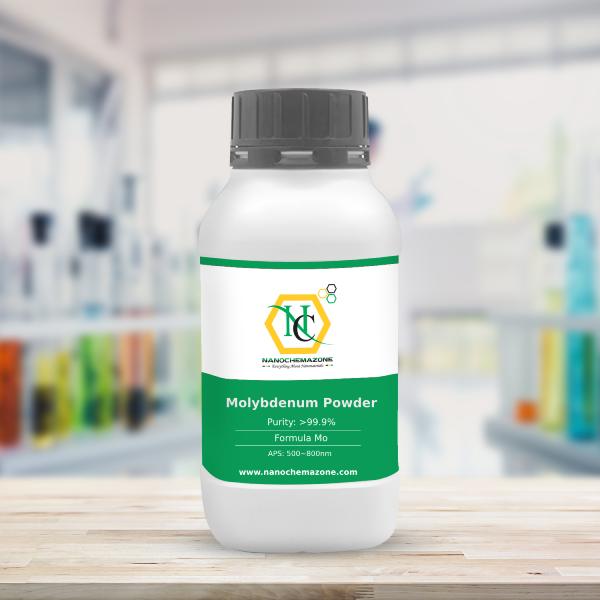
Molybdenum Powder ( 500~800nm, 99.9%)

Price range: $190.00 through $434.00
Select options This product has multiple variants. The options may be chosen on the product page
$190/100g
$305/500g
$434/1000g

Product 

Molybdenum Powder ( 500~800nm, 99.9%)

CAS No.

7439-98-7

Appearance

Powder

Purity

≥99%,  ≥99.9%,  ≥95%

(Other purities are also available)

APS

500~800nm (Size Can be customized), Ask for other available size ranges.

Ingredient

N/A

Molecular Weight

95.95 g/mol

Melting Point

~2623°C

Boiling Point

4639 °C

Density

10.28 g/cm³

Product Codes

NCZ-1050K

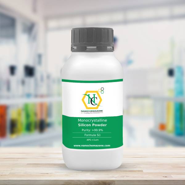
Monocrystalline Silicon Nanoparticles/ Nanopowder (Si, 99% 1um)

Price range: $190.00 through $815.00
Select options This product has multiple variants. The options may be chosen on the product page
$190/100g
$815/500g

Product 

Monocrystalline Silicon Nanoparticles/ Nanopowder (Si, 99% 1um)

CAS No.

7440-21-3

Appearance

Powder

Purity

≥99%,  ≥99.9%,  ≥95%

(Other purities are also available)

APS

1um(Size Can be customized), Ask for other available size ranges.

Ingredient

N/A

Molecular Weight

28.0855 g/mol

Melting Point

1,414 °C

Boiling Point

3,265 °C

Density

~2.33 g/cm³

Product Codes

NCZ-1067K

Monocrystalline Silicon Nanoflakes (Si, 97%, <1um)

Price range: $190.00 through $815.00
Select options This product has multiple variants. The options may be chosen on the product page
$190/100 g
$815/500g

Product 

 Monocrystalline Silicon Nanoflakes (Si, 97%, <1um)

CAS No.

7440-21-3

Appearance

Powder

Purity

≥99%,  ≥99.9%,  ≥95%

(Other purities are also available)

APS

<1um (Size Can be customized), Ask for other available size ranges.

Ingredient

N/A

Molecular Weight

28.0855 g/mol

Melting Point

1,414 °C

Boiling Point

3,265 °C

Density

~2.33 g/cm³

Product Codes

NCZ-1069K

Lithium Sulfide Powder( Li2S, 99.9%)

Price range: $190.00 through $415.00
Select options This product has multiple variants. The options may be chosen on the product page
$190/25g
$415/100g

Product 

Lithium Sulfide Powder( Li2S, 99.9%)

CAS No.

Appearance

Powder

Purity

≥99%,  ≥99.9%,  ≥95%

(Other purities are also available)

APS

 5 μm (Size Can be customized), Ask for other available size ranges.

Ingredient

N/A

Molecular Weight

 45.95 g/mol

Melting Point

~938 °C

Boiling Point

 ~1,372 °C

Density

~1.66 g/cm³

Product Codes

NCZ-1148K

Spherical Magnesium oxide(MgO, 99%) (127665)

$190.00
Select options This product has multiple variants. The options may be chosen on the product page
Spherical Magnesium oxide(MgO, 99%) (127665)
10, 20, 30, 40µmProduct Codes- NCZ-2681K

SBA-15(All Si) (862853)

Price range: $190.00 through $1,395.00
Select options This product has multiple variants. The options may be chosen on the product page
SBA-15(All Si) (862853)

Pore Size(nm) 3.2 All Si BET(m2/g) 600 - 800 Na2O(ppm) <1000 Relative Crystallinity(%) 95 Loss on Ignition(%) <5

Product Codes- NCZ-2718K

Tin (Sn) Sputtering Targets, Purity: 99.99%, Size: 2”, Thickness: 0.250”

$191.00

Product 

Tin (Sn) Sputtering Targets, Purity: 99.99%, Size: 2'', Thickness: 0.250''

CAS No.

7440-31-5

Appearance

Powder

Purity

≥99%,  ≥99.9%,  ≥95%

(Other purities are also available)

APS

N/A  (Size Can be customized), Ask for other available size ranges.

Ingredient

N/A

Molecular Weight

118.71 g/mol

Melting Point

231.93 °C

Boiling Point

2602 °C

Density

~7.31 g/cm³

Product Codes

NCZ-1642K

Nickel (Ni) Sputtering Targets, Purity: 99.995%, Size: 2”, Thickness: 0.125”

$191.00

Product 

Nickel (Ni) Sputtering Targets, Purity: 99.995%, Size: 2'', Thickness: 0.125''

CAS No.

7440-02-0

Appearance

Powder

Purity

≥99%,  ≥99.9%,  ≥95%

(Other purities are also available)

APS

 N/A (Size Can be customized), Ask for other available size ranges.

Ingredient

N/A

Molecular Weight

 58.69 g/mol

Melting Point

~1,453 °C

Boiling Point

~2,732 – 2,914 °C

Density

 8.90 g/cm³

Product Codes

NCZ-1890K

Silver Conductive Adhesive Paste

Price range: $192.00 through $3,915.00
Select options This product has multiple variants. The options may be chosen on the product page

Applications:

- Silver Conductive Adhesive Paste is mainly used as the conductive. - Silver Conductive Adhesive Paste is used for the backside of solar cell. - Silver Conductive Adhesive Paste is used  for inner electrode. - Silver Conductive Adhesive Paste also has good properties in damp-heat resistance and chemical. - Silver Conductive Adhesive Paste is widely used in home supplies.

Magnetic Graphene Aerogel, Content of Fe3O4: 65%, Diameter: 1±0.1 cm

Price range: $192.00 through $748.00
Select options This product has multiple variants. The options may be chosen on the product page
1 piece/ 192 € 5 pieces/ 748 €  Contact us for tailored quotes on larger quantities & experience exceptional solutions from our

Silver Conductive Adhesive Paste

Price range: $192.00 through $3,915.00
Select options This product has multiple variants. The options may be chosen on the product page

Applications:

- Silver Conductive Adhesive Paste is mainly used as the conductive. - Silver Conductive Adhesive Paste is used for the backside of solar cell. - Silver Conductive Adhesive Paste is used  for inner electrode. - Silver Conductive Adhesive Paste also has good properties in damp-heat resistance and chemical. - Silver Conductive Adhesive Paste is widely used in home supplies.

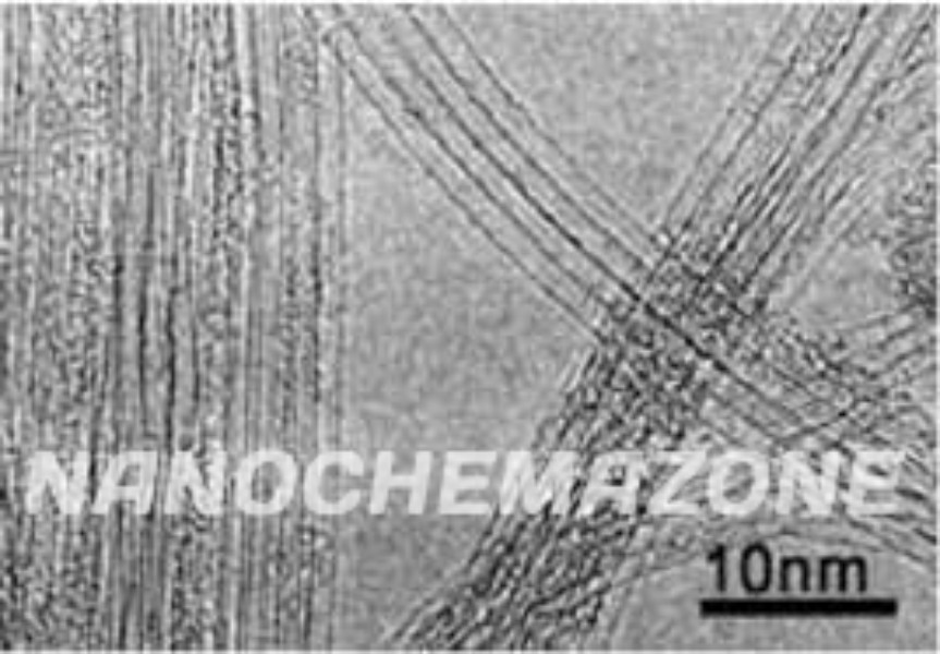
(-OH) Functionalized Short Single Walled Carbon Nanotubes, Purity: >92%

Price range: $193.00 through $2,809.00
Select options This product has multiple variants. The options may be chosen on the product page

Applications:

Single Walled Carbon Nanotubes have a variety of potential applications in different fields. These applications include medicine, mechanics, electric-electronics, chemicals, energy and others. It can be applied in, 1-drug delivery, 2-biosensors, 3-CNT composites, 4-catalysis, 5-nanoprobes, 6-hydrogen storage, 7-lithium batteries, 8-gas-discharge tubes, 9-flat panel displays, 10-supercapacitors, 11-transistors, 12-solar cells, 13-photoluminescence, 14-templates

Impending Self-Help Transfer Nickel Graphene Foam, Thickness: 1±0.1 mm, Size: 1×1 cm

Price range: $193.00 through $869.00
Select options This product has multiple variants. The options may be chosen on the product page
1 piece/ 193 € 5 pieces/ 869 €  Contact us for tailored quotes on larger quantities & experience exceptional solutions from our experts.

Fullerene-C70, Purity: 96%

Price range: $193.00 through $925.00
Select options This product has multiple variants. The options may be chosen on the product page

Applications:

1. Pharmaceutical: Diagnostic reagents, super drugs, cosmetics, nuclear magnetic resonance (NMR) with the developer. DNA affinity 2. Energy: Solar battery, fuel cell, secondary battery. 3. Industry: Wear resistant material, flame retardant materials, lubricants, polymer additives, high-performance membrane, catalyst, artificial diamond, hard alloy, electric viscous fluid, ink filters, high-performance coatings, fire retardant coatings, manufacturing bioactive materials , memory materials, embedded molecular and other characteristics, composite materials etc. 4. Information industry: Semiconductor record medium, magnetic materials, printing ink, toner, ink, paper special purposes. 5. Electronic parts: Superconducting semiconductor, diodes, transistors, inductor.  , 6. Optical materials, electronic camera, fluorescence display tube, nonlinear optical materials. 7. Environment: Gas adsorption, gas storage.

Bismuth Nanopowder/ Nanoparticles ( Bi, 99.9%, 100nm)

Price range: $193.00 through $585.00
Select options This product has multiple variants. The options may be chosen on the product page
$193/25g $585/100g

Product 

Bismuth Nanopowder/ Nanoparticles ( Bi, 99.9%, 100nm)

CAS No.

7440-69-9

Appearance

Powder

Purity

≥99%,  ≥99.9%,  ≥95%

(Other purities are also available)

APS

100nm (Size Can be customized), Ask for other available size ranges.

Ingredient

AlN

Molecular Weight

208.98 g/mol

Melting Point

~271.4 °C

Boiling Point

1,564 °C

Density

~9.78 g/cm³

Product Codes

NCZ-1021K

SWNTs -COOH Functionalized 90%

Price range: $193.00 through $885.00
Select options This product has multiple variants. The options may be chosen on the product page
$193/1g
$885/5g

Product 

SWNTs -COOH Functionalized 90%

CAS No.

1034343-98-0

Appearance

Powder

Purity

≥99%,  ≥99.9%,  ≥95%

(Other purities are also available)

APS

1-2 nm (Size Can be customized), Ask for other available size ranges.

Ingredient

N/A

Molecular Weight

NA

Melting Point

 >600 °C

Boiling Point

NA

Density

~1.3–1.4 g/cm³

Product Codes

NCZ-1268K

Silicon (Si) Sputtering Targets, undoped, Purity: 99.999%, Size: 2”, Thickness: 0.125”

$193.00

Product 

Silicon (Si) Sputtering Targets, undoped, Purity: 99.999%, Size: 2'', Thickness: 0.125''

CAS No.

7440-21-3

Appearance

Powder

Purity

≥99%,  ≥99.9%,  ≥95%

(Other purities are also available)

APS

N/A  (Size Can be customized), Ask for other available size ranges.

Ingredient

N/A

Molecular Weight

28.0855 g/mol

Melting Point

1,414 °C

Boiling Point

 3,265 °C

Density

 2.33 g/cm³

Product Codes

NCZ-1735K

Fullerene-C70, Purity: 98%

Price range: $194.00 through $940.00
Select options This product has multiple variants. The options may be chosen on the product page
1 gram/174 € 5 grams/840 €                           
Please contact us for quotes on larger quantities !!!

Fullerene-C70

Purity: 98% 

Technical Properties:

Fullerene Compound Formula C70
Fullerene  Molecular Weight 840.77 g/mol
Fullerene  Purity 98%
Fullerene  Melting Point >280 °C
Fullerene  Appearance Black Powder
Fullerene  CAS 115383-22-7

Applications:

1. Pharmaceutical: Diagnostic reagents, super drugs, cosmetics, nuclear magnetic resonance (NMR) with the developer. DNA affinity 2. Energy: Solar battery, fuel cell, secondary battery. 3. Industry: Wear resistant material, flame retardant materials, lubricants, polymer additives, high-performance membrane, catalyst, artificial diamond, hard alloy, electric viscous fluid, ink filters, high-performance coatings, fire retardant coatings, manufacturing bioactive materials , memory materials, embedded molecular and other characteristics, composite materials etc. 4. Information industry: Semiconductor record medium, magnetic materials, printing ink, toner, ink, paper special purposes. 5. Electronic parts: Superconducting semiconductor, diodes, transistors, inductor.  , 6. Optical materials, electronic camera, fluorescence display tube, nonlinear optical materials. 7. Environment: Gas adsorption, gas storage.

Magnetic Graphene Aerogel, Content of Fe3O4: 50%, Diameter: 1±0.1 cm

Price range: $194.00 through $753.00
Select options This product has multiple variants. The options may be chosen on the product page
1 piece/ 194 € 5 pieces/ 753 €  Contact us for tailored quotes on larger quantities & experience exceptional solutions from our experts.

Lithium Titanate (Li2TiO3) Sputtering Targets, Purity: 99.95%, Size: 1”, Thickness: 0.250”

$194.00

Applications of Sputtering Targets;

Film deposition is accomplished using sputtering targets. A technique for sputtering thin films is called "deposition made by sputter targets," which entails eroding material from a "target" source onto a "substrate" like a silicon wafer. Etching of the target is done using semiconductor sputtering targets. When selectivity is not an issue and a high degree of etching anisotropy is required, sputter etching is the method of choice. By removing the target material through etching, sputter targets are also utilized for investigation. In secondary ion spectroscopy (SIMS), one example is when the target material is sputtered at a steady pace. Mass spectrometry is used to quantify the concentration and identity of spewed atoms as the target is sputtered.

By helping of the sputtering target, the composition of the target material may be evaluated and even extremely tiny amounts of contaminants are recognized.

There is also an application area for sputtering targets in space. One type of space weathering that alters the chemical and physical characteristics of airless worlds like the Moon and asteroids is sputtering.

Zinc (Zn) Sputtering Targets, Purity: 99.95%, Size: 4”, Thickness: 0.125”

$194.00

Applications of Sputtering Targets;

Film deposition is accomplished using sputtering targets. A technique for sputtering thin films is called "deposition made by sputter targets," which entails eroding material from a "target" source onto a "substrate" like a silicon wafer. Etching of the target is done using semiconductor sputtering targets. When selectivity is not an issue and a high degree of etching anisotropy is required, sputter etching is the method of choice. By removing the target material through etching, sputter targets are also utilized for investigation. In secondary ion spectroscopy (SIMS), one example is when the target material is sputtered at a steady pace. Mass spectrometry is used to quantify the concentration and identity of spewed atoms as the target is sputtered.

The target material's composition may be ascertained and even very low concentrations of contaminants can be found with the aid of the sputtering target.

There is also an application area for sputtering targets in space. One type of space weathering that alters the chemical and physical characteristics of airless worlds like the Moon and asteroids is sputtering.

Aluminum (Al) Sputtering Targets, Purity: 99.99%, Size: 4”, Thickness: 0.125”

$194.00

Product 

Aluminum (Al) Sputtering Targets, Purity: 99.99%, Size: 4'', Thickness: 0.125''

CAS No.

7429‑90‑5

Appearance

Powder

Purity

≥99%,  ≥99.9%,  ≥95%

(Other purities are also available)

APS

Al (Size Can be customized), Ask for other available size ranges.

Ingredient

N/A

Molecular Weight

26.98 g/mol

Melting Point

660.3 °C

Boiling Point

2467 °C

Density

 2.70 g/cm³

Product Codes

NCZ-1402K

99.99% 4N 0.3-0.5 um Alpha Aluminum Oxide (Alumina) Al2O3 Powder, 500 g

$194.00
Product 99.99% 4N 0.3-0.5 um Alpha Aluminum Oxide (Alumina) Al2O3 Powder, 500 g
CAS No. 1344-28-1
Appearance White
Purity ≥99%,  ≥99.9%,  ≥95%(Other purities are also available)
APS 0.3-0.5um (Size Can be customized),  Ask for other available size range.
Ingredient Al2O3
Molecular Weight 101.96 g/mol
Melting Point 2,072 °C
Boiling Point N/A
Density 0.4–1.0 g/cm³
Product Codes NCZ-235I

Praseodymium (III, IV) Oxide (Pr6O11) 99.9% 3N Powder

Price range: $194.00 through $1,085.00
Select options This product has multiple variants. The options may be chosen on the product page
Product Praseodymium (III, IV) Oxide (Pr6O11) 99.9% 3N Powder
CAS No. 12037-29-5
Appearance Dark brown to black
Purity ≥99%,  ≥99.9%,  ≥95%(Other purities are also available)
APS 1–10µm (Size Can be customized),  Ask for other available size range.
Ingredient Pr6O11
Molecular Weight 1021.44 g/mol
Melting Point 2,180 °C
Boiling Point N/A
Density 6.5–6.9 g/cm³
Product Codes NCZ-498I

Iron (Fe) Sputtering Targets, Purity: 99.99%, Size: 4”, Thickness: 0.250”

$194.00

Product 

Iron (Fe) Sputtering Targets, Purity: 99.99%, Size: 4'', Thickness: 0.250''

CAS No.

 7439-89-6

Appearance

Powder

Purity

≥99%,  ≥99.9%,  ≥95%

(Other purities are also available)

APS

 N/A (Size Can be customized), Ask for other available size ranges.

Ingredient

N/A

Molecular Weight

 55.85 g/mol

Melting Point

 1538 °C

Boiling Point

 2862 °C

Density

 7.87 g/cm³

Product Codes

NCZ-2178K

Chromium Powder ( Cr, 99%, <=10um)

Price range: $195.00 through $345.00
Select options This product has multiple variants. The options may be chosen on the product page
$195/500g $345/1000g

Product 

Chromium Powder ( Cr, 99%, <=10um)

CAS No.

7440-47-3

Appearance

Powder

Purity

≥99%,  ≥99.9%,  ≥95%

(Other purities are also available)

APS

<=10um (Size Can be customized), Ask for other available size ranges.

Ingredient

AlN

Molecular Weight

51.9961 g/mol

Melting Point

1,907 °C

Boiling Point

2,672 °C

Density

7.19 g/cm³ (bulk)

Product Codes

NCZ-1030K

Holmium Oxide Powder (Ho2O3, 99.9%, 1-10um)

$195.00
Select options This product has multiple variants. The options may be chosen on the product page
$195/200g

Product 

Holmium Oxide Powder (Ho2O3, 99.9%, 1-10um)

CAS No.

12055-62-8

Appearance

Powder

Purity

≥99%,  ≥99.9%,  ≥95%

(Other purities are also available)

APS

1–10 µm (Size Can be customized), Ask for other available size ranges.

Ingredient

N/A

Molecular Weight

377.86 g/mol

Melting Point

 ~2,335 °C

Boiling Point

 ~3,900 °C

Density

 ~8.41 g/cm³

Product Codes

NCZ-1139K

Tungsten Disulfide Nanopowder/ Nanoparticles ( WS2, 99.9%, <100nm)

Price range: $195.00 through $1,045.00
Select options This product has multiple variants. The options may be chosen on the product page
$195/25g
$475/100g
$1045/500g

Product 

Tungsten Disulfide Nanopowder/ Nanoparticles ( WS2, 99.9%, <100nm)

CAS No.

12138-09-9

Appearance

Powder

Purity

≥99%,  ≥99.9%,  ≥95%

(Other purities are also available)

APS


<100nm (Size Can be customized), Ask for other available size ranges.

Ingredient

N/A

Molecular Weight

247.97 g/mol

Melting Point

~1,250 °C

Boiling Point

 ~2,295 °C

Density

 ~7.5 g/cm³

Product Codes

NCZ-1204K

High Purity Larger Surface Area SWNTs 95+%

Price range: $195.00 through $755.00
Select options This product has multiple variants. The options may be chosen on the product page
$195/1g
$755/5g

Product 

High Purity Larger Surface Area SWNTs 95+%

CAS No.

7727-54-0

Appearance

Powder

Purity

≥99%,  ≥99.9%,  ≥95%

(Other purities are also available)

APS

1-2 nm (Size Can be customized), Ask for other available size ranges.

Ingredient

N/A

Molecular Weight

228.20 g/mol

Melting Point

~3,650 °C

Boiling Point

N/A

Density

1.98 g/cm³

Product Codes

NCZ-1238K

Titanium Carbide (Ti2CTx) MXene Multilayer Nanoflakes

Price range: $195.00 through $1,536.00
Select options This product has multiple variants. The options may be chosen on the product page
Product Titanium Carbide (Ti2CTx) MXene Multilayer Nanoflakes
CAS No. 12363-89-2
Appearance Grey to black
Purity ≥99%,  ≥99.9%,  ≥95%(Other purities are also available)
APS 2–15µm (Size Can be customized),  Ask for other available size range.
Ingredient Ti2CTx
Molecular Weight 160.47 g/mol
Melting Point N/A
Boiling Point N/A
Density N/A
Product Codes NCZ-575I

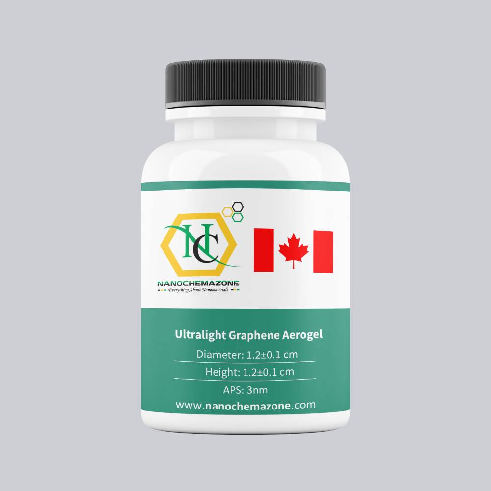
Ultralight Graphene Aerogel, Diameter: 1.2±0.1 cm, Height: 1.2±0.1 cm

Price range: $196.00 through $743.00
Select options This product has multiple variants. The options may be chosen on the product page
1 piece/ 196 € 5 pieces/ 743 € Contact us for tailored quotes on larger quantities & experience exceptional solutions from our experts.

Copper Nanowires immersed in ethanol

$197.00
Select options This product has multiple variants. The options may be chosen on the product page
$197/5g

Product 

Copper Nanowires immersed in ethanol

CAS No.

7440-50-8

Appearance

Powder

Purity

≥99%,  ≥99.9%,  ≥95%

(Other purities are also available)

APS

150 nm (Size Can be customized), Ask for other available size ranges.

Ingredient

AlN

Molecular Weight

63.55 g/mol

Melting Point

1084.62 °C

Boiling Point

2562 °C

Density

8.96 g/cm³

Product Codes

NCZ-1038K

Impending Self-Help Transfer Nickel Graphene Foam, Thickness: 1±0.1 mm, Size: 1×1 cm

Price range: $198.00 through $896.00
Select options This product has multiple variants. The options may be chosen on the product page
Please contact us for quotes for larger quantities !   Impending self-help transfer nickel graphene foam is produced by etching the nickel of nickel graphene foam in etching liquid and being transferred to impending substrate. Graphene foam, can be gently released in deionized water and transferred directly to any base. This product is widely used for producing sensors, super capacitors and as the electrode materials of lithium battery to improve the battery capacity.

Magnetic Graphene Aerogel, Content of Fe3O4: 65%, Diameter: 1±0.1 cm

Price range: $198.00 through $769.00
Select options This product has multiple variants. The options may be chosen on the product page
Please contact us for quotes for larger quantities !   This aerogel is a self-assembled, 3d porous foam material with high quality sheet layer < 3 graphene oxide and Fe3O4 nanoparticles as raw materials. The aerogel has micron-sized macropores and nano-sized mesoporous pores to form a rich compound void structure. With stable chemical properties, large specific surface area and abundant pores, this aerogel is suitable for the adsorption of copper, chromium, lead and other heavy metals in water.

Carbon-Coated Aluminum Foil

Price range: $198.00 through $844.00
Select options This product has multiple variants. The options may be chosen on the product page
Product Specification Item Specification Product Name Carbon-Coated Aluminum Foil Substrate Aluminum Foil Substrate Thickness 20μm Foil Substrate Width 210±0.5mm Foil Substrate Length

Lithium Cobalt Oxide (LiCoO2) Coated Aluminum Foil

Price range: $198.00 through $845.00
Select options This product has multiple variants. The options may be chosen on the product page
Product Specification Item Specification Product Name Lithium Cobalt Oxide (LiCoO2) Coated Aluminum Foil Substrate Aluminum Foil Substrate Thickness 20μm Foil Substrate

Lithium Iron Phosphate (LiFePO4) Coated Aluminum Foil

Price range: $198.00 through $844.00
Select options This product has multiple variants. The options may be chosen on the product page
Product Specification   Item Specification Product Name Lithium Iron Phosphate (LiFePO4) Coated Aluminum Foil Substrate Aluminum Foil Substrate Thickness 20μm Foil

Carbon-Coated Aluminum Foil

Price range: $198.00 through $844.00
Select options This product has multiple variants. The options may be chosen on the product page
Product Specification Item Specification Product Name Carbon-Coated Aluminum Foil Substrate Aluminum Foil Substrate Thickness 20μm Foil Substrate Width 210±0.5mm Foil Substrate Length

Lithium Cobalt Oxide (LiCoO2) Coated Aluminum Foil

Price range: $198.00 through $845.00
Select options This product has multiple variants. The options may be chosen on the product page
Product Specification Item Specification Product Name Lithium Cobalt Oxide (LiCoO2) Coated Aluminum Foil Substrate Aluminum Foil Substrate Thickness 20μm Foil Substrate

Lithium Iron Phosphate (LiFePO4) Coated Aluminum Foil

Price range: $198.00 through $844.00
Select options This product has multiple variants. The options may be chosen on the product page
Product Specification   Item Specification Product Name Lithium Iron Phosphate (LiFePO4) Coated Aluminum Foil Substrate Aluminum Foil Substrate Thickness 20μm Foil

Silver (Ag) Sputtering Targets, Purity: 99.99%, Size: 1”, Thickness: 0.250”

$198.00

Applications of Sputtering Targets;

Film deposition is accomplished using sputtering targets. A technique for sputtering thin films is called "deposition made by sputter targets," which entails eroding material from a "target" source onto a "substrate" like a silicon wafer. Etching of the target is done using semiconductor sputtering targets. When selectivity is not an issue and a high degree of etching anisotropy is required, sputter etching is the method of choice. By removing the target material through etching, sputter targets are also utilized for investigation. In secondary ion spectroscopy (SIMS), one example is when the target material is sputtered at a steady pace. Mass spectrometry is used to quantify the concentration and identity of spewed atoms as the target is sputtered.

The target material's composition may be ascertained and even very low concentrations of contaminants can be found with the aid of the sputtering target.

There is also an application area for sputtering targets in space. One type of space weathering that alters the chemical and physical characteristics of airless worlds like the Moon and asteroids is sputtering.

30 nm 8YSZ Zirconium Dioxide ZrO2 Nanoparticles,>86.5% High Purity

Price range: $198.00 through $2,189.00
Select options This product has multiple variants. The options may be chosen on the product page
Product 30 nm 8YSZ Zirconium Dioxide ZrO2 Nanoparticles,>86.5% High Purity
CAS No. 1314-23-4
Appearance White or off-white
Purity ≥99%,  ≥99.9%,  ≥95%(Other purities are also available)
APS 30nm (Size Can be customized), Ask for other available size range.
Ingredient ZrO2 
Molecular Weight 123.22 g/mol
Melting Point N/A
Boiling Point N/A
Density 5.2 g/cm³
Product Codes NCZ-151I