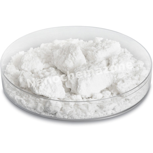
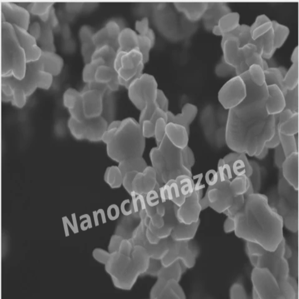
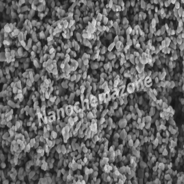
Germanium (Ge) Sputtering Targets, Purity: 99.999%, Size: 2”, Thickness: 0.125”

$180.00

Product 

Germanium (Ge) Sputtering Targets, Purity: 99.999%, Size: 2'', Thickness: 0.125''

CAS No.

7440‑56‑4

Appearance

Powder

Purity

≥99%,  ≥99.9%,  ≥95%

(Other purities are also available)

APS

Ge (Size Can be customized), Ask for other available size ranges.

Ingredient

N/A

Molecular Weight

72.63 g/mol

Melting Point

937.4 °C

Boiling Point

2,830 °C

Density

 ~5.32 g/cm³

Product Codes

NCZ-1399K

99.9wt% Hierarchical Porous Silica Microspheres Powder, 400 nm-900 nm

Price range: $180.00 through $330.00
Select options This product has multiple variants. The options may be chosen on the product page
Product 99.9wt% Hierarchical Porous Silica Microspheres Powder, 400 nm-900 nm
CAS No. 7631-86-9
Appearance White or off-white fine
Purity ≥99%,  ≥99.9%,  ≥95%(Other purities are also available)
APS 400-900nm (Size Can be customized),  Ask for other available size range.
Ingredient SiO₂
Molecular Weight 60.08 g/mol
Melting Point N/A
Boiling Point N/A
Density 2.0–2.2 g/cm³
Product Codes NCZ-271I

Nickel Vanadium (NiV) Sputtering Targets, Purity: 99.95%, Size: 1”, Thickness: 0.125”

$180.00

Product 

Nickel Vanadium (NiV) Sputtering Targets, Purity: 99.95%, Size: 1'', Thickness: 0.125''

CAS No.

11137-91-4

Appearance

Powder

Purity

≥99%,  ≥99.9%,  ≥95%

(Other purities are also available)

APS

N/A (Size Can be customized), Ask for other available size ranges.

Ingredient

N/A

Molecular Weight

~57.9 g/mol

Melting Point

~1,350–1,450 °C

Boiling Point

N/A

Density

 ~8.5 g/cm³

Product Codes

NCZ-1830K

Chitosan(Food grade) (332668)

$180.00
Select options This product has multiple variants. The options may be chosen on the product page
Chitosan(Food grade) (332668)
Item
Food grade
Appearance
White powder
Degree of deacetylation
90%, 95%
pH
7.0-8.0
Loss on drying
<10.0%
Residue on ignition
<1.5%
Insoluble
<1.0%
Heavy metal (measured by Pb)
≤10ppm
As
≤0.5ppm
Total bacterial count
≤1000cfu/g
Viscosity 50-800mpa·s
Granularity 80mesh, 100mesh
Product Codes- NCZ-2654K

Nisin(1000IU, 30000IU) (526557)

Price range: $180.00 through $770.00
Select options This product has multiple variants. The options may be chosen on the product page
Nisin(1000IU, 30000IU) (526557)
  • ITEM DESCRIPTION
    Product Name Nisin 2.5% in NaCl for 1000IU/mg Nisin 75% in NaCl for 30000IU/mg
    Titer 1000IU/mg, 30000IU/mg
    Strain Lactococcus lactis subsp lactis
    Appearance White or Off white to light brown powder
    EU No. E234
    Molecular Formula C143H228N42O37S7
    CAS 1414-45-5
    Solubility 5-10g/100ml in pH=2.5-3.5 of aqueous for 1000IU/mg 0.1g/100ml in pH=2.5-3.5 of aqueous for 30000IU/mg
    Stability pH 2.5-3.5 Nisin is relatively stable. pH 3.5-6.5 100°C 30minutes, Nisin is less stable, but the stability will be improved when Nisin is existing with food proteins. pH>7.0 Nisin is comparatively less stable
    Carrier NaCl 50.0% Min for 1000IU/mg NaCl 6.0% Min for 30000IU/mg
    Moisture 3.0% Max.
    Heavy Metals Not more than 10mg/Kg
    Usage The additive may be applied in cheese, desserts, yoghurt, processed meat, fruit and vegetable juices, bakeries, egg products and canned food
    pH pH=3.3-3.8, 10% solution for 1000IU/mg pH=3.0-3.8, 10% solution for 30000IU/mg
    Total colony count Mesophillic aerobic not more than 10 CFU/g
    E-Coli. 25g Negative
    Saimonelia 25g Negative
    Storage Nisin is stable under room temperature. Sunlight, oxidant and heavy metal will hurt the activity of it. To be stored in dry , shady and cool place(below 20°C)with sealed packing
    Shelf life 24 months
 
Product Codes- NCZ-2790K

(-OH) Functionalized Short Length Double Walled Carbon Nanotubes, Purity: > 65%

Price range: $181.00 through $2,581.00
Select options This product has multiple variants. The options may be chosen on the product page

Applications:

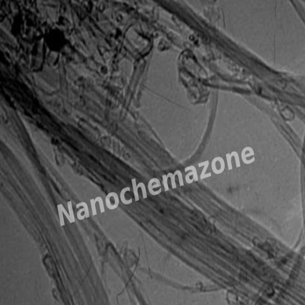
Double Walled Carbon Nanotubes have a variety of potential applications in different fields. These applications include medicine, mechanics, electric-electronics, chemicals, energy and others. It can be applied in, 1-drug delivery, 2-biosensors, 3-CNT composites, 4-catalysis, 5-nanoprobes, 6-hydrogen storage, 7-lithium batteries, 8-gas-discharge tubes, 9-flat panel displays, 10-supercapacitors, 11-transistors, 12-solar cells, 13-photoluminescence, 14-templates

Single Layer Graphene Oxide, Purity: 99.5 %

Price range: $181.00 through $1,804.00
Select options This product has multiple variants. The options may be chosen on the product page

Applications of Single Layer Graphene Oxide

  • Energy Storage
  • Biomedical Applications
  • Biosensors

Magnesium (Mg) Sputtering Targets, Purity: 99.98%, Size: 2”, Thickness: 0.125”

$181.00

Applications of Sputtering Targets;

Film deposition is accomplished using sputtering targets. A technique for sputtering thin films is called "deposition made by sputter targets," which entails eroding material from a "target" source onto a "substrate" like a silicon wafer. Etching of the target is done using semiconductor sputtering targets. When selectivity is not an issue and a high degree of etching anisotropy is required, sputter etching is the method of choice. By removing the target material through etching, sputter targets are also utilized for investigation. In secondary ion spectroscopy (SIMS), one example is when the target material is sputtered at a steady pace. Mass spectrometry is used to quantify the concentration and identity of spewed atoms as the target is sputtered.

By helping of the sputtering target, the composition of the target material may be evaluated and even extremely tiny amounts of contaminants are recognized.

There is also an application area for sputtering targets in space. One type of space weathering that alters the chemical and physical characteristics of airless worlds like the Moon and asteroids is sputtering.

Prime CZ-Si Wafer, Size: 8”, Orientation: (100), Boron Doped, Resistivity: 1000-10000 (ohm.cm), 1-Side Polished, Thickness: 725 ± 25 μm

Price range: $182.00 through $3,795.00
Select options This product has multiple variants. The options may be chosen on the product page
1 piece/163 € 5 pieces/710 € 25 pieces/3390 € Please contact us for quotes on larger quantities !!!

Prime CZ-Si Wafer

Size: 8”, Orientation: (100), Boron Doped, 1-Side Polished, Thickness: 725 ± 25 μm

Technical Properties:

Quality Prime
Materials CZ-Si
Size (inch) 8”
Orientation (100)
Coating  
Thickness (μm) 725 ± 25 μm
Doping Boron
Resistivity (ohm.cm) 1000-10000
Polished One Side
Silicon is one of the most common elements on earths crust. Main usage of Silicon wafers is electronics and technology. Silicon wafers have very flat and mirror like surfaces. It is produced by Czochralski method to obtain the highest purity. Depending on the usage area, silicon wafers can be doped with different materials to tailor its purity accordingly. The amount and type of dopants highly affect the electronic properties. Galium, indium, boron and nitrogen are some of the dopants that can be used in production process. Silicon wafers are used in semiconductors, microchips, integrated circuits, smartphones, computers etc. Silicon is the key platform for semiconductor gadgets. A wafer is just but a thin slice of the semiconductor material that acts as a substratum for microelectronic devices fitted in and above the wafer.

CR2016 Coin Cell Cases with 304SS (Positive+Negative Cases), Diameter: 20 mm, Height : 1.6 mm

Price range: $182.00 through $1,238.00
Select options This product has multiple variants. The options may be chosen on the product page
100 set:182€ 500 set: 800€ 1000 set:1238€ Technical Properties: Diameter 20 mm Height 1.6 mm Material 304SS

CR2325 Coin Cell Cases with 304SS (Positive+Negative Cases), Diameter: 23 mm, Height : 2.5 mm

Price range: $182.00 through $1,238.00
Select options This product has multiple variants. The options may be chosen on the product page
100 set:182€ 500 set: 800€ 1000 set:1238€ Technical Properties: Diameter 23 mm Height 2.5 mm Material 304SS  

Antimony (Sb) Sputtering Targets, Purity: 99.95%, Size: 2”, Thickness: 0.250”

$182.00

Applications of Sputtering Targets;

Film deposition is accomplished using sputtering targets. A technique for sputtering thin films is called "deposition made by sputter targets," which entails eroding material from a "target" source onto a "substrate" like a silicon wafer. Etching of the target is done using semiconductor sputtering targets. When selectivity is not an issue and a high degree of etching anisotropy is required, sputter etching is the method of choice. By removing the target material through etching, sputter targets are also utilized for investigation. In secondary ion spectroscopy (SIMS), one example is when the target material is sputtered at a steady pace. When the target shatters,

Mass spectrometry measures the concentration and identity of sputtered atoms. The target material's composition may be ascertained and even very low concentrations of contaminants can be found with the aid of the sputtering target.

There is also an application area for sputtering targets in space. One type of space weathering that alters the chemical and physical characteristics of airless worlds like the Moon and asteroids is sputtering.

Group 15 of the periodic table contains antimony (Sb), which shares an atomic number of 51 with bismuth and arsenic. It gleams with a metallic sheen. bluish-white in color. Despite not having the same reputation as a poison, antimony shares many of the same chemical characteristics as arsenic. Its average natural abundance in the earth's crust is 0.2 to 0.5 parts per million. Antimony sputtering targets can be utilized to create fire-retardant coatings since antimony has excellent fire retardance properties. Antimony sputtering targets can also be utilized for optoelectronic devices such as solar cells, laser diodes, photodiodes, and LEDs.

Zinc (Zn) Sputtering Targets, Purity: 99.95%, Size: 2”, Thickness: 0.250”

$183.00

Product 

Zinc (Zn) Sputtering Targets, Purity: 99.95%, Size: 2'', Thickness: 0.250''

CAS No.

7440‑66‑6

Appearance

Powder

Purity

≥99%,  ≥99.9%,  ≥95%

(Other purities are also available)

APS

Zn (black granules) (Size Can be customized), Ask for other available size ranges.

Ingredient

N/A

Molecular Weight

65.38 g/mol

Melting Point

419.5 °C

Boiling Point

 907 °C

Density

7.14 g/cm³

Product Codes

NCZ-1472K

50-100 nm Yttrium (III) Oxide (Y2O3) 99.999% 5N Nano Powder

Price range: $183.00 through $755.00
Select options This product has multiple variants. The options may be chosen on the product page
Product 50-100 nm Yttrium (III) Oxide (Y2O3) 99.999% 5N Nano Powder
CAS No. 1314-36-9
Appearance White
Purity ≥99%,  ≥99.9%,  ≥95%(Other purities are also available)
APS 50-100nm (Size Can be customized),  Ask for other available size range.
Ingredient Y2O3
Molecular Weight N/A
Melting Point 2425 °C
Boiling Point N/A
Density 5.01 g/cm³
Product Codes NCZ-184I

Erbium Chloride Hexahydrate (ErCl3 · 6H2O) 99.5% 2N5

$183.00
Select options This product has multiple variants. The options may be chosen on the product page
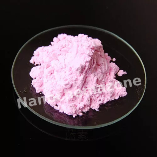
Product Erbium Chloride Hexahydrate (ErCl3 · 6H2O) 99.5% 2N5
CAS No. 10025-75-9
Appearance Pink crystalline
Purity ≥99%,  ≥99.9%,  ≥95%(Other purities are also available)
APS 50–100µm (Size Can be customized),  Ask for other available size range.
Ingredient ErCl3·6H2O
Molecular Weight 381.71 g/mol
Melting Point N/A
Boiling Point N/A
Density N/A
Product Codes NCZ-341I

Europium (III) Oxide (Eu2O3) 99.999% 5N Powder

Price range: $183.00 through $1,085.00
Select options This product has multiple variants. The options may be chosen on the product page
Product Europium (III) Oxide (Eu2O3) 99.999% 5N Powder
CAS No. 1308-96-9
Appearance White
Purity ≥99%,  ≥99.9%,  ≥95%(Other purities are also available)
APS 10–100µm (Size Can be customized),  Ask for other available size range.
Ingredient Eu2O3
Molecular Weight 351.296  g/mol
Melting Point 2350°C
Boiling Point N/A
Density 7.42 g/cm³
Product Codes NCZ-343I
 

Lithium Titanate (Li2TiO3) Sputtering Targets, Purity: 99.95%, Size: 1”, Thickness: 0.125”

$183.00

Product 

Lithium Titanate (Li2TiO3) Sputtering Targets, Purity: 99.95%, Size: 1'', Thickness: 0.125''

CAS No.

12031-82-2

Appearance

Powder

Purity

≥99%,  ≥99.9%,  ≥95%

(Other purities are also available)

APS

 N/A (Size Can be customized), Ask for other available size ranges.

Ingredient

N/A

Molecular Weight

109.75 g/mol

Melting Point

Decomposes before melting (~1,200 °C)

Boiling Point

N/A

Density

~3.41 g/cm³

Product Codes

NCZ-2015K

Tin (IV) Sulfide, SnS2, 99.5% Powder, 100g

$183.00
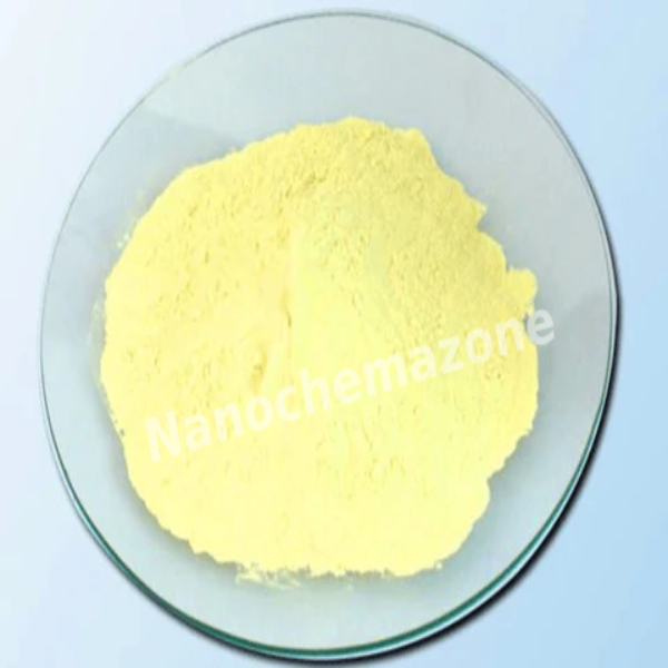
Product Tin (IV) Sulfide, SnS2, 99.5% Powder, 100g
CAS No. 1315-01-1
Appearance Gold-yellow
Purity ≥99%,  ≥99.9%,  ≥95%(Other purities are also available)
APS N/A
Ingredient SnS2
Molecular Weight N/A
Melting Point 600 °C
Boiling Point N/A
Density 4.5 g/cm³
Product Codes NCZ-564I
 

Titanium (IV) Dioxide (TiO2) Anatase 99.8% 2N8 Nano Powder 50 nm

Price range: $183.00 through $315.00
Select options This product has multiple variants. The options may be chosen on the product page
Product Titanium (IV) Dioxide (TiO2) Anatase 99.8% 2N8 Nano Powder 50 nm
CAS No. 13463-67-7
Appearance White fine
Purity ≥99%,  ≥99.9%,  ≥95%(Other purities are also available)
APS 50nm (Size Can be customized),  Ask for other available size range.
Ingredient TiO2
Molecular Weight 79.87 g/mol
Melting Point N/A
Boiling Point N/A
Density 3.9–4.1 g/cm³
Product Codes NCZ-569I

Aluminum Silicon (AlSi) Sputtering Targets, Purity: 99.999%, Size: 2”, Thickness: 0.250”

$184.00

Applications of Sputtering Targets;

Film deposition is accomplished using sputtering targets. A technique for sputtering thin films is called "deposition made by sputter targets," which entails eroding material from a "target" source onto a "substrate" like a silicon wafer. Etching of the target is done using semiconductor sputtering targets. When selectivity is not an issue and a high degree of etching anisotropy is required, sputter etching is the method of choice. By removing the target material through etching, sputter targets are also utilized for investigation. In secondary ion spectroscopy (SIMS), one example is when the target material is sputtered at a steady pace. When the target shatters,

Mass spectrometry measures the concentration and identity of sputtered atoms. The target material's composition may be ascertained and even very low concentrations of contaminants can be found with the aid of the sputtering target.

There is also an application area for sputtering targets in space. One type of space weathering that alters the chemical and physical characteristics of airless worlds like the Moon and asteroids is sputtering.

Nickel Iron (Ni-Fe) Sputtering Targets, Purity: 99.5%, Size: 2”, Thickness: 0.125”

$184.00

Applications of Sputtering Targets;

Film deposition is accomplished using sputtering targets. A technique for sputtering thin films is called "deposition made by sputter targets," which entails eroding material from a "target" source onto a "substrate" like a silicon wafer. Etching of the target is done using semiconductor sputtering targets. When selectivity is not an issue and a high degree of etching anisotropy is required, sputter etching is the method of choice. By removing the target material through etching, sputter targets are also utilized for investigation. In secondary ion spectroscopy (SIMS), one example is when the target material is sputtered at a steady pace. Mass spectrometry is used to quantify the concentration and identity of spewed atoms as the target is sputtered.

The target material's composition may be ascertained and even very low concentrations of contaminants can be found with the aid of the sputtering target.

There is also an application area for sputtering targets in space. One type of space weathering that alters the chemical and physical characteristics of airless worlds like the Moon and asteroids is sputtering.

Niobium (Nb) Sputtering Targets, Purity: 99.95% pure Ex Ta, Size: 3”, Thickness: 0.125”

$184.00

Applications of Sputtering Targets;

Film deposition is accomplished using sputtering targets. A technique for sputtering thin films is called "deposition made by sputter targets," which entails eroding material from a "target" source onto a "substrate" like a silicon wafer. Etching of the target is done using semiconductor sputtering targets. When selectivity is not an issue and a high degree of etching anisotropy is required, sputter etching is the method of choice. By removing the target material through etching, sputter targets are also utilized for investigation. In secondary ion spectroscopy (SIMS), one example is when the target material is sputtered at a steady pace. Mass spectrometry is used to quantify the concentration and identity of spewed atoms as the target is sputtered.

The target material's composition may be ascertained and even very low concentrations of contaminants can be found with the aid of the sputtering target.

There is also an application area for sputtering targets in space. One type of space weathering that alters the chemical and physical characteristics of airless worlds like the Moon and asteroids is sputtering.

Niobium (Nb) Sputtering Targets, Purity: 99.95% pure Ex Ta, Size: 4”, Thickness: 0.125”

$184.00

Applications of Sputtering Targets;

Film deposition is accomplished using sputtering targets. A technique for sputtering thin films is called "deposition made by sputter targets," which entails eroding material from a "target" source onto a "substrate" like a silicon wafer. Etching of the target is done using semiconductor sputtering targets. When selectivity is not an issue and a high degree of etching anisotropy is required, sputter etching is the method of choice. By removing the target material through etching, sputter targets are also utilized for investigation. In secondary ion spectroscopy (SIMS), one example is when the target material is sputtered at a steady pace. Mass spectrometry is used to quantify the concentration and identity of spewed atoms as the target is sputtered.

The target material's composition may be ascertained and even very low concentrations of contaminants can be found with the aid of the sputtering target.

There is also an application area for sputtering targets in space. One type of space weathering that alters the chemical and physical characteristics of airless worlds like the Moon and asteroids is sputtering.

Vanadium (V) Sputtering Targets, Purity: 99.5%, Size: 2”, Thickness: 0.125”

$184.00

Applications of Sputtering Targets;

Film deposition is accomplished using sputtering targets. A technique for sputtering thin films is called "deposition made by sputter targets," which entails eroding material from a "target" source onto a "substrate" like a silicon wafer. Etching of the target is done using semiconductor sputtering targets. When selectivity is not an issue and a high degree of etching anisotropy is required, sputter etching is the method of choice. By removing the target material through etching, sputter targets are also utilized for investigation. In secondary ion spectroscopy (SIMS), one example is when the target material is sputtered at a steady pace. Mass spectrometry is used to quantify the concentration and identity of spewed atoms as the target is sputtered.

The target material's composition may be ascertained and even very low concentrations of contaminants can be found with the aid of the sputtering target.

There is also an application area for sputtering targets in space. One type of space weathering that alters the chemical and physical characteristics of airless worlds like the Moon and asteroids is sputtering.

Zinc (Zn) Sputtering Targets, Purity: 99.99%, Size: 3”, Thickness: 0.250”

$184.00

Applications of Sputtering Targets;

Film deposition is accomplished using sputtering targets. A technique for sputtering thin films is called "deposition made by sputter targets," which entails eroding material from a "target" source onto a "substrate" like a silicon wafer. Etching of the target is done using semiconductor sputtering targets. When selectivity is not an issue and a high degree of etching anisotropy is required, sputter etching is the method of choice. By removing the target material through etching, sputter targets are also utilized for investigation. In secondary ion spectroscopy (SIMS), one example is when the target material is sputtered at a steady pace. Mass spectrometry is used to quantify the concentration and identity of spewed atoms as the target is sputtered.

The target material's composition may be ascertained and even very low concentrations of contaminants can be found with the aid of the sputtering target.

There is also an application area for sputtering targets in space. One type of space weathering that alters the chemical and physical characteristics of airless worlds like the Moon and asteroids is sputtering.

Zinc (Zn) Sputtering Targets, Purity: 99.95%, Size: 3”, Thickness: 0.125”

$184.00

Applications of Sputtering Targets;

Film deposition is accomplished using sputtering targets. A technique for sputtering thin films is called "deposition made by sputter targets," which entails eroding material from a "target" source onto a "substrate" like a silicon wafer. Etching of the target is done using semiconductor sputtering targets. When selectivity is not an issue and a high degree of etching anisotropy is required, sputter etching is the method of choice. By removing the target material through etching, sputter targets are also utilized for investigation. In secondary ion spectroscopy (SIMS), one example is when the target material is sputtered at a steady pace. Mass spectrometry is used to quantify the concentration and identity of spewed atoms as the target is sputtered.

The target material's composition may be ascertained and even very low concentrations of contaminants can be found with the aid of the sputtering target.

There is also an application area for sputtering targets in space. One type of space weathering that alters the chemical and physical characteristics of airless worlds like the Moon and asteroids is sputtering.

Zinc (Zn) Sputtering Targets, Purity: 99.95%, Size: 3”, Thickness: 0.125”

$184.00

Applications of Sputtering Targets;

Film deposition is accomplished using sputtering targets. A technique for sputtering thin films is called "deposition made by sputter targets," which entails eroding material from a "target" source onto a "substrate" like a silicon wafer. Etching of the target is done using semiconductor sputtering targets. When selectivity is not an issue and a high degree of etching anisotropy is required, sputter etching is the method of choice. By removing the target material through etching, sputter targets are also utilized for investigation. In secondary ion spectroscopy (SIMS), one example is when the target material is sputtered at a steady pace. Mass spectrometry is used to quantify the concentration and identity of spewed atoms as the target is sputtered.

The target material's composition may be ascertained and even very low concentrations of contaminants can be found with the aid of the sputtering target.

There is also an application area for sputtering targets in space. One type of space weathering that alters the chemical and physical characteristics of airless worlds like the Moon and asteroids is sputtering.

Magnesium (Mg) Sputtering Target

Price range: $184.00 through $507.00
Select options This product has multiple variants. The options may be chosen on the product page

Product 

Magnesium (Mg) Sputtering Target

CAS No.

7439-92-1

Appearance

Powder

Purity

≥99%,  ≥99.9%,  ≥95%

(Other purities are also available)

APS

 NA (Size Can be customized), Ask for other available size ranges.

Ingredient

N/A

Molecular Weight

24.305 g/mol

Melting Point

650 °C

Boiling Point

1,090 °C

Density

1.738 g/cm³

Product Codes

NCZ-1296K

Tungsten Titanium Sputtering Target WTi

Price range: $184.00 through $879.00
Select options This product has multiple variants. The options may be chosen on the product page
Product Tungsten Titanium Sputtering Target WTi
CAS No. 58397-70-9
Appearance Grayish-white lustrous
Purity ≥99%,  ≥99.9%,  ≥95%(Other purities are also available)
APS N/A
Ingredient WTi
Molecular Weight 231.71 g/mol
Melting Point N/A
Boiling Point N/A
Density 10.4 - 12.0 g/cm³
Product Codes NCZ-146H

Nickel (Ni) Sputtering Targets, Purity: 99.99%, Size: 4”, Thickness: 0.125”

$184.00

Product 

Nickel (Ni) Sputtering Targets, Purity: 99.99%, Size: 4'', Thickness: 0.125''

CAS No.

7440-02-0

Appearance

Powder

Purity

≥99%,  ≥99.9%,  ≥95%

(Other purities are also available)

APS

 N/A (Size Can be customized), Ask for other available size ranges.

Ingredient

N/A

Molecular Weight

 58.69 g/mol

Melting Point

 1,455 °C

Boiling Point

 2,732 °C

Density

 8.90 g/cm³

Product Codes

NCZ-1879K

Nickel (Ni) Sputtering Targets, Purity: 99.99%, Size: 2”, Thickness: 0.250”

$184.00

Product 

Nickel (Ni) Sputtering Targets, Purity: 99.99%, Size: 2'', Thickness: 0.250''

CAS No.

7440-02-0

Appearance

Powder

Purity

≥99%,  ≥99.9%,  ≥95%

(Other purities are also available)

APS

 N/A (Size Can be customized), Ask for other available size ranges.

Ingredient

N/A

Molecular Weight

 58.69 g/mol

Melting Point

~1,453 °C

Boiling Point

~2,913 °C

Density

 8.90 g/cm³

Product Codes

NCZ-1888K

Fullerene-C70, Purity: 95%

Price range: $185.00 through $838.00
Select options This product has multiple variants. The options may be chosen on the product page

Applications:

1. Pharmaceutical: Diagnostic reagents, super drugs, cosmetics, nuclear magnetic resonance (NMR) with the developer. DNA affinity 2. Energy: Solar battery, fuel cell, secondary battery. 3. Industry: Wear resistant material, flame retardant materials, lubricants, polymer additives, high-performance membrane, catalyst, artificial diamond, hard alloy, electric viscous fluid, ink filters, high-performance coatings, fire retardant coatings, manufacturing bioactive materials , memory materials, embedded molecular and other characteristics, composite materials etc. 4. Information industry: Semiconductor record medium, magnetic materials, printing ink, toner, ink, paper special purposes. 5. Electronic parts: Superconducting semiconductor, diodes, transistors, inductor. 6. Optical materials, electronic camera, fluorescence display tube, nonlinear optical materials. 7. Environment: Gas adsorption, gas storage.

Erbium Oxide Powder ( Er2O3 Powder, 99.5%, -200 mesh)

$185.00
Select options This product has multiple variants. The options may be chosen on the product page
$185/500g

Product 

Erbium Oxide Powder ( Er2O3 Powder, 99.5%, -200 mesh)

CAS No.

12061-16-4

Appearance

Powder

Purity

≥99%,  ≥99.9%,  ≥95%

(Other purities are also available)

APS

-200 mesh (Size Can be customized), Ask for other available size ranges.

Ingredient

N/A

Molecular Weight

382.52 g/mol

Melting Point

~2,340 °C

Boiling Point

~3,800 °C

Density

~8.64 g/cm³

Product Codes

NCZ-1132K

Phosphorus Pentasulfide Powder( P2S5, 99.9%)

Price range: $185.00 through $405.00
Select options This product has multiple variants. The options may be chosen on the product page
$185/25g
$405/100g

Product 

Phosphorus Pentasulfide Powder( P2S5, 99.9%)

CAS No.

1314-80-3

Appearance

Powder

Purity

≥99%,  ≥99.9%,  ≥95%

(Other purities are also available)

APS

5 – 50 µm (Size Can be customized), Ask for other available size ranges.

Ingredient

N/A

Molecular Weight

222.27 g/mol

Melting Point

 ~288 °C

Boiling Point

Decomposes before boiling (~514 °C in vacuum)

Density

~2.09 g/cm³

Product Codes

NCZ-1161K

Cerium Carbonate (Ce2(CO3)3) 99.95% 3N5

Price range: $185.00 through $1,340.00
Select options This product has multiple variants. The options may be chosen on the product page
Product Cerium Carbonate (Ce2(CO3)3) 99.95% 3N5
CAS No. 51341-60-7
Appearance White to off-white
Purity ≥99%,  ≥99.9%,  ≥95%(Other purities are also available)
APS N/A
Ingredient Ce2(CO3)3
Molecular Weight 460.23 g/mol
Melting Point N/A
Boiling Point N/A
Density 5.13 g/cm³
Product Codes NCZ-313I

(-COOH) Functionalized Short Length Double Walled Carbon Nanotubes, Purity: > 65%

Price range: $186.00 through $2,876.00
Select options This product has multiple variants. The options may be chosen on the product page

Applications:

Double Walled Carbon Nanotubes have a variety of potential applications in different fields. These applications include medicine, mechanics, electric-electronics, chemicals, energy and others. It can be applied in, 1-drug delivery, 2-biosensors, 3-CNT composites, 4-catalysis, 5-nanoprobes, 6-hydrogen storage, 7-lithium batteries, 8-gas-discharge tubes, 9-flat panel displays, 10-supercapacitors, 11-transistors, 12-solar cells, 13-photoluminescence, 14-templates

Single Layer Graphene Oxide, Purity: 99.5 %, Size: 1 nm

Price range: $186.00 through $1,856.00
Select options This product has multiple variants. The options may be chosen on the product page
Single layer graphene oxide is a mono-atomic layer of highly oxidized carbon atoms, manufactured by chemical oxidation of graphite. Graphene oxide layers are about 1.1 ± 0.2 nm thick. Monolayer graphne oxide can be embedded in different ceramic or polymeric matrices to enhance electrical, thermal and mechanical properties. Thanks to its excellent properties of single-layer graphene oxide, it has been involved in many applications such as Graphene and polymers manufacture, water purification, flexible rechargeable battery electrode, optically transparent films, papers, sensors, nanocarriers for metal catalysis, anti-electrostatic additives and many more. We are committed to provide high quality single layer graphene oxide with competitive prices and fast shipping.

Gallium Arsenide (GaAs) Wafers, Size: 4”, Thickness: 600±25 μm, Double Side Polished, EPI-ready

Price range: $186.00 through $4,385.00
Select options This product has multiple variants. The options may be chosen on the product page
1 piece/168€ 5 pieces/830€ 25 pieces/3950€ Please contact us for quotes on larger quantities ! Gallium Arsenide (GaAs) Wafer Size: 4”, Double Side Polished, Thickness: 600± 25 μm, EPI-ready Technical Properties:
Quality  GaAs
Materials  GaAs
Size (inch)  4”
Thickness (μm)  600± 25
Polished  Double Side
Dopant  Undoped
Orientation  (100) 
Resistivity   1 E8
Mobility  4500
EPD  ≤5000
Growth method  VGF
OF Length  32,5±1
IF Length  18±1
Applications: Gallium arsenide (GaAs) is a compound of the elements gallium and arsenic. Vertical gradient freeze is the most common method to produce GaAs wafers. Mainly used for circuits, electronics and solar cell applications. Carbon, silicon, tellurium and zinc are some of the dopants that are used to modify the characteristics and electrical properties of gallium arsenide wafers. Wafer flatness and surface purity are ensured by highest quality standards. Boron concentration of gallium arsenide wafers highly depend on the production method. Gallium arsenide wafers with adequate electrical resistancy prevent high current induction in the circuit. Mobility of GaAs wafers can be tailored with different doping levels. Gallium arsenide (GaAs) is a semiconductor compound. Gallium arsenide (GaAs)  has a high electron velocity and high saturated electron mobility. This makes gallium arsenide (GaAs) components are useful in fast electronic switching applications and at ultra-high radio frequencies. In 1907, the British discovered infrared emmission from gallium arsenide. This was called electroluminescence. Also, gallium arsenide (GaAs) was used as a solar cells in space for the Venera 3 mission in 1965, which is the first known operational use of gallium arsenide (GaAs).
  • Gallium arsenide (GaAs) is used in laser diodes.
  • Gallium arsenide (GaAs) is used in solar cells.
  • Gallium arsenide (GaAs) is used in optical windows.
  • Gallium arsenide (GaAs) is used in monolithic microwave integrated circuits.
  • Gallium arsenide (GaAs) is used in microwave frequency integrated circuits.
  • Gallium arsenide (GaAs) is used in infrared light-emitting diodes.
  • Gallium arsenide (GaAs) is useful in barometers.
  • Gallium arsenide (GaAs) is useful in pharmaceuticals and nuclear medicine tests.
  • Gallium arsenide (GaAs) is useful in high temperature thermometers.

Erbium Oxide (Er2O3) Sputtering Targets, Purity: 99.99%, Size: 3”, Thickness: 0.250”

$186.00
Select options This product has multiple variants. The options may be chosen on the product page

Applications of Sputtering Targets;

  • Sputtering targets is used for film deposition. The deposition made by sputter targets is a method of depositing thin films by sputtering that involves eroding material from a "target" source onto a "substrate" such as  a silicon wafer.
  • Semiconductor sputtering targets is used to etch the target. Sputter etching is chosen in cases where a high degree of etching anisotropy is needed and selectivity is not a concern.
  • Sputter targets is also used for analysis by etching away the target material.
One of the example occurs in secondary ion spectroscopy (SIMS), where the target sample is sputtered at a constant rate. As the target is sputtered, the concentration and identity of sputtered atoms are measured using mass spectrometry. By helping of the sputtering target, the composition of the target material can be determined and even extremely low concentrations of impurities are detected. Sputtering target has also application area in space. Sputtering is one of the forms of space weathering, a process that changes the physical and chemical properties of airless bodies, such as asteroids and the Moon. Erbium oxide with a chemical formula of Er2Ois an oxide of erbium metal. The applications of erbium oxide are varied due to their electrical, optical and photoluminescence properties. Nanoscale materials doped with Er+3 are of much interest because they have special particle-size-dependent optical and electrical properties. Erbium oxide doped nanoparticle materials can be dispersed in glass or plastic for display purposes, such as display monitors. The spectroscopy of Er+3 electronic transitions in host crystals lattices of nanoparticles combined with ultrasonically formed geometries in aqueous solution of carbon nanotubes is of great interest for synthesis of photoluminescence nanoparticles in ‘green’ chemistry. Erbium oxide is among the most important rare earth metals used in biomedicine. Erbium oxides are also used as gate dielectrics in semiconductor devices since it has a high dielectric constant (10-14) and a large band gap. Erbium is sometimes used as a coloring for glasses and erbium oxide can also be used as a burnable neutron poison for nuclear fuel. Erbium oxide films obtained by sputtering can be used for their photoluminescence effect.

Erbium Oxide (Er2O3) Sputtering Targets, Purity: 99.99%, Size: 3”, Thickness: 0.250”

$186.00

Applications of Sputtering Targets;

Film deposition is accomplished using sputtering targets. A technique for sputtering thin films is called "deposition made by sputter targets," which entails eroding material from a "target" source onto a "substrate" like a silicon wafer. Etching of the target is done using semiconductor sputtering targets. When selectivity is not an issue and a high degree of etching anisotropy is required, sputter etching is the method of choice. By removing the target material through etching, sputter targets are also utilized for investigation. In secondary ion spectroscopy (SIMS), one example is when the target material is sputtered at a steady pace. Mass spectrometry is used to quantify the concentration and identity of spewed atoms as the target is sputtered.

The target material's composition may be ascertained and even very low concentrations of contaminants can be found with the aid of the sputtering target.

There is also an application area for sputtering targets in space. One type of space weathering that alters the chemical and physical characteristics of airless worlds like the Moon and asteroids is sputtering.

Erbium Oxide (Er2O3) Sputtering Targets, Purity: 99.99%, Size: 3”, Thickness: 0.250”

$186.00

Applications of Sputtering Targets;

Film deposition is accomplished using sputtering targets. A technique for sputtering thin films is called "deposition made by sputter targets," which entails eroding material from a "target" source onto a "substrate" like a silicon wafer. Etching of the target is done using semiconductor sputtering targets. When selectivity is not an issue and a high degree of etching anisotropy is required, sputter etching is the method of choice. By removing the target material through etching, sputter targets are also utilized for investigation. In secondary ion spectroscopy (SIMS), one example is when the target material is sputtered at a steady pace. Mass spectrometry is used to quantify the concentration and identity of spewed atoms as the target is sputtered.

The target material's composition may be ascertained and even very low concentrations of contaminants can be found with the aid of the sputtering target.

There is also an application area for sputtering targets in space. One type of space weathering that alters the chemical and physical characteristics of airless worlds like the Moon and asteroids is sputtering.

Niobium (Nb) Sputtering Targets, Purity: 99.95% pure Ex Ta, Size: 3”, Thickness: 0.250”

$186.00

Applications of Sputtering Targets;

Film deposition is accomplished using sputtering targets. A technique for sputtering thin films is called "deposition made by sputter targets," which entails eroding material from a "target" source onto a "substrate" like a silicon wafer. Etching of the target is done using semiconductor sputtering targets. When selectivity is not an issue and a high degree of etching anisotropy is required, sputter etching is the method of choice. By removing the target material through etching, sputter targets are also utilized for investigation. In secondary ion spectroscopy (SIMS), one example is when the target material is sputtered at a steady pace. Mass spectrometry is used to quantify the concentration and identity of spewed atoms as the target is sputtered.

The target material's composition may be ascertained and even very low concentrations of contaminants can be found with the aid of the sputtering target.

There is also an application area for sputtering targets in space. One type of space weathering that alters the chemical and physical characteristics of airless worlds like the Moon and asteroids is sputtering.

3N (99.9%) Tin Oxide (SnO2) Pieces (3-12mm) Evaporation Materials

Price range: $186.00 through $484.00
Select options This product has multiple variants. The options may be chosen on the product page
Product 3N (99.9%) Tin Oxide (SnO2) Pieces (3-12mm) Evaporation Materials
CAS No. 18282-10-5
Appearance White or Gray, Crystalline Solid
Purity ≥99%,  ≥99.9%,  ≥95%(Other purities are also available)
APS 3-12mm (Size Can be customized),  Ask for other available size range.
Ingredient SnO2
Molecular Weight 150.71 g/mol
Melting Point 1,700 °C
Boiling Point N/A
Density 6.95 g/cm3
Product Codes NCZ-152E

Yttrium Fluoride (YF3) 99.9% 3N

Price range: $186.00 through $556.00
Select options This product has multiple variants. The options may be chosen on the product page
Product Yttrium Fluoride (YF3) 99.9% 3N
CAS No. 13758-39-7
Appearance White crystalline
Purity ≥99%,  ≥99.9%,  ≥95%(Other purities are also available)
APS N/A
Ingredient YF3
Molecular Weight 169.91 g/mol
Melting Point N/A
Boiling Point N/A
Density 5.03 g/cm³
Product Codes NCZ-605I

Silicon Hexaboride (SiB6) Nanopowder, APS: 40nm, Purity: 99%

Price range: $187.00 through $1,572.00
Select options This product has multiple variants. The options may be chosen on the product page
Silicon Hexaboride (SiB6) Nanopowder,  APS: 40nm, Purity: 99% Performance characteristics Nano silicon hexaboride powder is prepared by high-frequency plasma gas phase synthesis. It is a gray-black powder with a relative density of 3.0g/cm3 and a melting point of 2200°C. It is insoluble in water, resistant to oxidation, thermal shock, and chemical attack. It has high strength and stability especially under thermal shock, and the grinding efficiency is higher than that of boron carbide. Applications 1. It can be used as various standard abrasives and grinding cemented carbides; 2. It is also used as engineering ceramic materials, sandblasting nozzles, blades of gas engines and other special-shaped sintered parts and seals; 3. Used as an anti-oxidant for refractory materials; 4. Add in powder metallurgy and cemented carbide to improve strength, hardness, and heat resistance; 5. Used in aerospace carbon-carbon composite materials to improve the ablation resistance and high temperature strength of composite materials. Packaging and storage This product is packaged in an inert gas plastic bag, sealed and stored in a dry, cool environment. It should not be exposed to the air to prevent oxidation and agglomeration due to moisture, which will affect the dispersion performance and use effect; the number of packages can be provided according to customer requirements and packed.
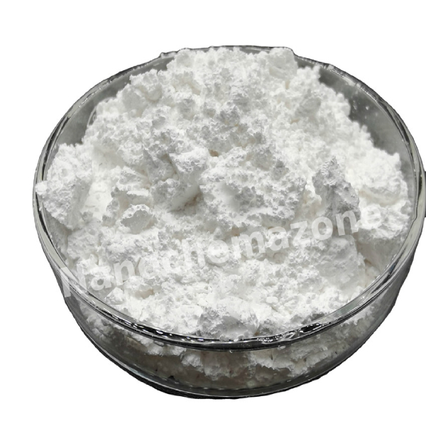
Aluminum (Al) Sputtering Targets, Purity: 99.99%, Size: 4”, Thickness: 0.250”

$187.00

Applications of Sputtering Targets;

  • Sputtering targets is used for film deposition. The deposition made by sputter targets is a method of depositing thin films by sputtering that involves eroding material from a "target" source onto a "substrate" such as  a silicon wafer.
  • Semiconductor sputtering targets is used to etch the target. Sputter etching is chosen in cases where a high degree of etching anisotropy is needed and selectivity is not a concern.
  • Sputter targets is also used for analysis by etching away the target material.
One of the example occurs in secondary ion spectroscopy (SIMS), where the target sample is sputtered at a constant rate. As the target is sputtered, the concentration and identity of sputtered atoms are measured using mass spectrometry. By helping of the sputtering target, the composition of the target material can be determined and even extremely low concentrations of impurities are detected. Sputtering target has also application area in space. Sputtering is one of the forms of space weathering, a process that changes the physical and chemical properties of airless bodies, such as asteroids and the Moon. Aluminum which has the chemical symbol of Al, is a silvery white, soft, ductile metal that is the third most abundant element. Aluminum is notable due to for its light weight, strength, durability and for its ability to resist corrosion. Aluminum forms an extremely thin but very strong layer of oxide film. Aluminum has also high thermal and electrical conductivity. Aluminum sputtering targets have a particularly fine-grained microstructure. This property of Aluminum sputtering targets ensures that you benefit from uniform erosion and a low susceptibility to particle formation throughout the sputtering process.

Strontium Carbonate Nanopowder/ Nanoparticles ( SrCO3, < 500nm, 99+% Nanopowder)

Price range: $187.00 through $417.00
Select options This product has multiple variants. The options may be chosen on the product page
$187/100g
$417/500g

Product 

Strontium Carbonate Nanopowder/ Nanoparticles ( SrCO3, < 500nm, 99+% Nanopowder)

CAS No.

18282-10-5

Appearance

Powder

Purity

≥99%,  ≥99.9%,  ≥95%

(Other purities are also available)

APS

10~15nm (Size Can be customized), Ask for other available size ranges.

Ingredient

N/A

Molecular Weight

~150–165 g/mol

Melting Point

~1630 °C

Boiling Point

N/A

Density

 6.9–7.1 g/cm³

Product Codes

NCZ-1191K

Cobalt (Co) Sputtering Target

Price range: $187.00 through $555.00
Select options This product has multiple variants. The options may be chosen on the product page

Product 

Cobalt (Co) Sputtering Target

CAS No.

7440-48-4

Appearance

Powder

Purity

≥99%,  ≥99.9%,  ≥95%

(Other purities are also available)

APS

 NA (Size Can be customized), Ask for other available size ranges.

Ingredient

N/A

Molecular Weight

58.93 g/mol

Melting Point

 1,495 °C

Boiling Point

2,927 °C

Density

8.90 g/cm³

Product Codes

NCZ-1351K

Graphite (C) Sputtering Target

Price range: $187.00 through $555.00
Select options This product has multiple variants. The options may be chosen on the product page

Product 

Graphite (C) Sputtering Target

CAS No.

7782-42-5

Appearance

Powder

Purity

≥99%,  ≥99.9%,  ≥95%

(Other purities are also available)

APS

 NA (Size Can be customized), Ask for other available size ranges.

Ingredient

N/A

Molecular Weight

12.01 g/mol

Melting Point

~3,642 °C

Boiling Point

N/A

Density

~2.26 g/cm³

Product Codes

NCZ-1356K

Nickel (Ni) Sputtering Target

Price range: $187.00 through $555.00
Select options This product has multiple variants. The options may be chosen on the product page

Product 

Nickel (Ni) Sputtering Target

CAS No.

 7440-02-0

Appearance

Powder

Purity

≥99%,  ≥99.9%,  ≥95%

(Other purities are also available)

APS

 NA (Size Can be customized), Ask for other available size ranges.

Ingredient

N/A

Molecular Weight

 58.69 g/mol

Melting Point

 1,455 °C

Boiling Point

 2,913 °C

Density

 8.90 g/cm³

Product Codes

NCZ-1357K

99.8% 15-20 nm Rutile Titanium Dioxide TiO2 Nanoparticles, 500g

$187.00
Product 99.8% 15-20 nm Rutile Titanium Dioxide TiO2 Nanoparticles, 500g
CAS No. 1317-80-2
Appearance White
Purity ≥99%,  ≥99.9%,  ≥95%(Other purities are also available)
APS 15-20nm (Size Can be customized),  Ask for other available size range.
Ingredient TiO2
Molecular Weight N/A
Melting Point 1843 °C
Boiling Point N/A
Density 4.23 g/cm³
Product Codes NCZ-222I

99.8% 30-50 nm Rutile Titanium Dioxide TiO2 Nanoparticles, 500g

$187.00
Product 99.8% 30-50 nm Rutile Titanium Dioxide TiO2 Nanoparticles, 500g
CAS No. 1317-80-2
Appearance White
Purity ≥99%,  ≥99.9%,  ≥95%(Other purities are also available)
APS 30-50nm (Size Can be customized),  Ask for other available size range.
Ingredient TiO2
Molecular Weight N/A
Melting Point 1843 °C
Boiling Point N/A
Density 4.23 g/cm³
Product Codes NCZ-223I

99.8% 50-60 nm Rutile Titanium Dioxide TiO2 Nanoparticles, 500g

$187.00
Product 99.8% 50-60 nm Rutile Titanium Dioxide TiO2 Nanoparticles, 500g
CAS No. 1317-80-2
Appearance White
Purity ≥99%,  ≥99.9%,  ≥95%(Other purities are also available)
APS 50-60nm (Size Can be customized),  Ask for other available size range.
Ingredient TiO2
Molecular Weight N/A
Melting Point 1843 °C
Boiling Point N/A
Density 4.23 g/cm³
Product Codes NCZ-224I

99.8% 80-100 nm Titanium Dioxide TiO2 Rutile Nanoparticles, 500g

$187.00
Product 99.8% 80-100 nm Titanium Dioxide TiO2 Rutile Nanoparticles, 500g
CAS No. 1317-80-2
Appearance White
Purity ≥99%,  ≥99.9%,  ≥95%(Other purities are also available)
APS 80-100nm (Size Can be customized),  Ask for other available size range.
Ingredient TiO2
Molecular Weight N/A
Melting Point 1843 °C
Boiling Point N/A
Density 4.23 g/cm³
Product Codes NCZ-226I

Niobium (Nb) Sputtering Targets, Purity: 99.95% pure Ex Ta, Size: 2”, Thickness: 0.125”

$187.00

Product 

Niobium (Nb) Sputtering Targets, Purity: 99.95% pure Ex Ta, Size: 2'', Thickness: 0.125''

CAS No.

7440-03-1

Appearance

Powder

Purity

≥99%,  ≥99.9%,  ≥95%

(Other purities are also available)

APS

N/A (Size Can be customized), Ask for other available size ranges.

Ingredient

N/A

Molecular Weight

92.906 g/mol

Melting Point

 2,468 °C

Boiling Point

 4,744 °C

Density

 8.57 g/cm³

Product Codes

NCZ-1818K

Double-Walled Carbon Nanotubes, 1g

Price range: $187.00 through $253.00
Select options This product has multiple variants. The options may be chosen on the product page
Product Double-Walled Carbon Nanotubes, 1g
CAS No. 308068-56-6
Appearance Black fibrous
Purity ≥99%,  ≥99.9%,  ≥95%(Other purities are also available)
APS 2–5nm (Size Can be customized),  Ask for other available size range.
Ingredient CₓHᵧ
Molecular Weight N/A
Melting Point N/A
Boiling Point N/A
Density 2.1 g/cm³
Product Codes NCZ-337I
 

Molybdenum (Mo) Sputtering Targets, Purity: 99.95%, Size: 2”, Thickness: 0.250”

$187.00

Product 

Molybdenum (Mo) Sputtering Targets, Purity: 99.95%, Size: 2'', Thickness: 0.250''

CAS No.

 7439-98-7

Appearance

Powder

Purity

≥99%,  ≥99.9%,  ≥95%

(Other purities are also available)

APS

 N/A (Size Can be customized), Ask for other available size ranges.

Ingredient

N/A

Molecular Weight

95.95 g/mol

Melting Point

 2623 °C

Boiling Point

 4639 °C

Density

10.28 g/cm³

Product Codes

NCZ-1938K

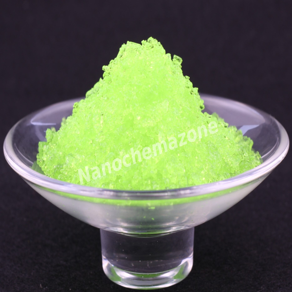
Praseodymium Nitrate Hexahydrate (Pr(NO3)3 · 6H2O) 99% 2N

Price range: $187.00 through $847.00
Select options This product has multiple variants. The options may be chosen on the product page
Product Praseodymium Nitrate Hexahydrate (Pr(NO3)3 · 6H2O) 99% 2N
CAS No. 15012-76-5
Appearance Light green crystalline
Purity ≥99%,  ≥99.9%,  ≥95%(Other purities are also available)
APS 10–50µm (Size Can be customized),  Ask for other available size range.
Ingredient Pr(NO3)3·6H2O
Molecular Weight 438.92 g/mol
Melting Point N/A
Boiling Point N/A
Density 2.3–2.5 g/cm³
Product Codes NCZ-503I
 

Aluminum (Al) Sputtering Targets, Purity: 99.999%, Size: 3”, Thickness: 0.125”

$187.00

Product 

Aluminum (Al) Sputtering Targets, Purity: 99.999%, Size: 3'', Thickness: 0.125''

CAS No.

 7429-90-5

Appearance

Powder

Purity

≥99%,  ≥99.9%,  ≥95%

(Other purities are also available)

APS

N/A (Size Can be customized), Ask for other available size ranges.

Ingredient

N/A

Molecular Weight

 26.98 g/mol

Melting Point

 660.3 °C

Boiling Point

 2519 °C

Density

 2.70 g/cm³

Product Codes

NCZ-2576K

Aluminum (Al) Sputtering Targets, Purity: 99.99%, Size: 3”, Thickness: 0.125”

$187.00

Product 

Aluminum (Al) Sputtering Targets, Purity: 99.99%, Size: 3'', Thickness: 0.125''

CAS No.

 7429-90-5

Appearance

Powder

Purity

≥99%,  ≥99.9%,  ≥95%

(Other purities are also available)

APS

N/A (Size Can be customized), Ask for other available size ranges.

Ingredient

N/A

Molecular Weight

 26.98 g/mol

Melting Point

 660.3 °C

Boiling Point

 2519 °C

Density

 2.70 g/cm³

Product Codes

NCZ-2577K