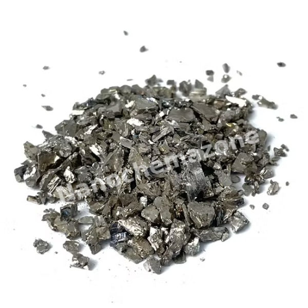
3N5 (99.95%) Magnesium Fluoride (MgF2) Pieces (1-3 mm) Evaporation Materials

Price range: $143.00 through $264.00
Select options This product has multiple variants. The options may be chosen on the product page
Product 3N5 (99.95%) Magnesium Fluoride (MgF2) Pieces (1-3 mm) Evaporation Materials
CAS No. 7783-40-6
Appearance White, Crystalline Solid 
Purity ≥99%,  ≥99.9%,  ≥95%(Other purities are also available)
APS 1-3mm (Size Can be customized),  Ask for other available size range.
Ingredient MgF2
Molecular Weight 62.30 g/mol
Melting Point N/A
Boiling Point N/A
Density 3.15 g/cm³
Product Codes NCZ-124E
 

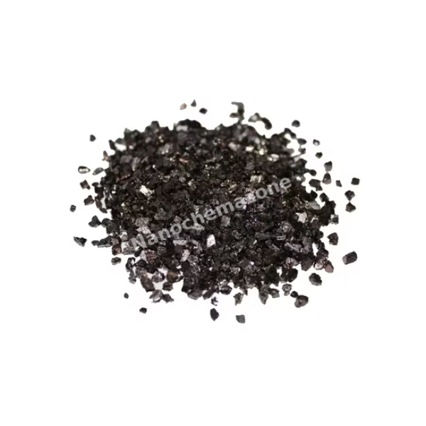
4N (99.99%) Boron (B) 3-8mm Pieces Evaporation Materials

Price range: $143.00 through $704.00
Select options This product has multiple variants. The options may be chosen on the product page
Product 4N (99.99%) Boron (B) 3-8mm Pieces Evaporation Materials
CAS No. 7440-42-8
Appearance Black, Semi-metallic
Purity ≥99%,  ≥99.9%,  ≥95%(Other purities are also available)
APS 3–8mm (Size Can be customized),  Ask for other available size range.
Ingredient B
Molecular Weight 10.81 g/mol
Melting Point 2,079 °C
Boiling Point N/A
Density 2.34 g/cm3
Product Codes NCZ-149E
 

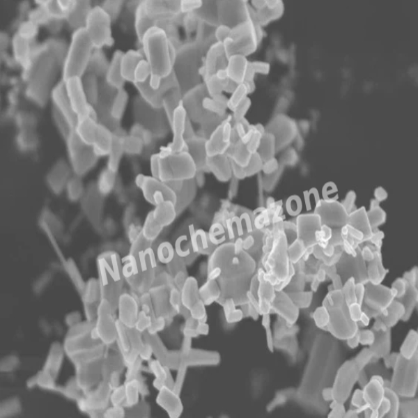
10nm Monoclinic Zirconium Dioxide ZrO2 Nanoparticles, >99.9% High Purity

Price range: $143.00 through $1,969.00
Select options This product has multiple variants. The options may be chosen on the product page
Product 10nm Monoclinic Zirconium Dioxide ZrO2 Nanoparticles, >99.9% High Purity
CAS No. 1314-23-4
Appearance White
Purity ≥99%,  ≥99.9%,  ≥95%(Other purities are also available)
APS 10nm (Size Can be customized),  Ask for other available size range.
Ingredient ZrO₂
Molecular Weight 123.22 g/mol
Melting Point N/A
Boiling Point N/A
Density 5.68–5.89 g/cm³
Product Codes NCZ-135I

30nm Monoclinic Zirconium Dioxide ZrO2 Nanoparticles, >99.9% High Purity

Price range: $143.00 through $1,969.00
Select options This product has multiple variants. The options may be chosen on the product page
Product 30nm Monoclinic Zirconium Dioxide ZrO2 Nanoparticles, >99.9% High Purity
CAS No. 1344-28-1
Appearance White
Purity ≥99%,  ≥99.9%,  ≥95%(Other purities are also available)
APS 30nm (Size Can be customized), Ask for other available size range.
Ingredient ZrO2
Molecular Weight N/A
Melting Point N/A
Boiling Point N/A
Density N/A
Product Codes NCZ-155I
 

4N (99.99%) Boron (B) 3-8mm Pieces Evaporation Materials

Price range: $143.00 through $704.00
Select options This product has multiple variants. The options may be chosen on the product page
Product 4N (99.99%) Boron (B) 3-8mm Pieces Evaporation Materials
CAS No. 7440-42-8
Appearance Black, brittle, crystalline
Purity ≥99%,  ≥99.9%,  ≥95%(Other purities are also available)
APS 3-8mm (Size Can be customized),  Ask for other available size range.
Ingredient B
Molecular Weight 123.22 g/mol
Melting Point 2,076 °C
Boiling Point 3,927 °C
Density 2.46 g/cm³
Product Codes NCZ-166I

99.9% Monoclinic Zirconia Polishing Powder Nanoparticles, 1kg

Price range: $143.00 through $539.00
Select options This product has multiple variants. The options may be chosen on the product page
Product 99.9% Monoclinic Zirconia Polishing Powder Nanoparticles, 1kg
CAS No. 1314-23-4
Appearance White
Purity ≥99%,  ≥99.9%,  ≥95%(Other purities are also available)
APS 20–100nm (Size Can be customized),  Ask for other available size range.
Ingredient ZrO₂
Molecular Weight 123.22 g/mol
Melting Point 2715 °C
Boiling Point N/A
Density 5.68 g/cm³
Product Codes NCZ-230I

Praseodymium (Pr) Sputtering Targets, Purity: 99.9%, Size: 2”, Thickness: 0.125”

$143.00

Product 

Praseodymium (Pr) Sputtering Targets, Purity: 99.9%, Size: 2'', Thickness: 0.125''

CAS No.

7440-10-0

Appearance

Powder

Purity

≥99%,  ≥99.9%,  ≥95%

(Other purities are also available)

APS

N/A (Size Can be customized), Ask for other available size ranges.

Ingredient

N/A

Molecular Weight

 140.91 g/mol

Melting Point

931 °C

Boiling Point

 3520 °C

Density

 6.77 g/cm³

Product Codes

NCZ-1793K

Gadolinium (III) Oxide (Gd2O3) 99.999% 5N Powder

Price range: $143.00 through $1,239.00
Select options This product has multiple variants. The options may be chosen on the product page
Product Gadolinium (III) Oxide (Gd2O3) 99.999% 5N Powder
CAS No. 12064-62-9
Appearance White odorless
Purity ≥99%,  ≥99.9%,  ≥95%(Other purities are also available)
APS 20–80nm (Size Can be customized),  Ask for other available size range.
Ingredient Gd2O3
Molecular Weight 362.50 g/mol
Melting Point N/A
Boiling Point N/A
Density 7.07 g/cm³
Product Codes NCZ-349I
 

High Purity Cerium Oxide (CeO2) Powder 99.999% 5N Trace Metal Basis

Price range: $143.00 through $403.00
Select options This product has multiple variants. The options may be chosen on the product page
Product High Purity Cerium Oxide (CeO2) Powder 99.999% 5N Trace Metal Basis
CAS No. 12061-16-4
Appearance Pale pink to lavender
Purity ≥99%,  ≥99.9%,  ≥95%(Other purities are also available)
APS 40–50nm (Size Can be customized),  Ask for other available size range.
Ingredient CeO2
Molecular Weight 382.52 g/mol
Melting Point N/A
Boiling Point N/A
Density N/A
Product Codes NCZ-409I

Strontium Fluoride (SrF2) 99%, 1kg

$143.00
Select options This product has multiple variants. The options may be chosen on the product page
Product Strontium Fluoride (SrF2) 99%, 1kg
CAS No. 7783-48-4
Appearance White crystalline
Purity ≥99%,  ≥99.9%,  ≥95%(Other purities are also available)
APS 10µm (Size Can be customized),  Ask for other available size range.
Ingredient SrF2
Molecular Weight 125.62 g/mol
Melting Point 1477 °C
Boiling Point N/A
Density 4.24 g/cm³
Product Codes NCZ-541I
 

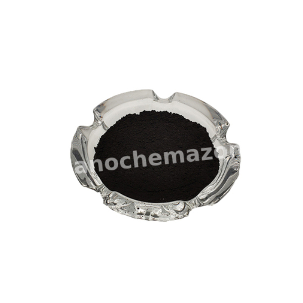
Titanium (III) Oxide (Ti2O3) 99.99% 4N Powder

Price range: $143.00 through $1,393.00
Select options This product has multiple variants. The options may be chosen on the product page
Product Titanium (III) Oxide (Ti2O3) 99.99% 4N Powder
CAS No. 1344-54-3
Appearance Violet-black
Purity ≥99%,  ≥99.9%,  ≥95%(Other purities are also available)
APS 5µm (Size Can be customized),  Ask for other available size range.
Ingredient Ti2O3
Molecular Weight 143.73–143.76 g/mol
Melting Point N/A
Boiling Point N/A
Density 4.49–4.6 g/cm³
Product Codes NCZ-568I
 

Zinc Oxide (ZnO) Nanoparticles, 30nm, 50nm, 90nm nano powders, >99.9% Purity

Price range: $143.00 through $165.00
Select options This product has multiple variants. The options may be chosen on the product page
Product Zinc Oxide (ZnO) Nanoparticles, 30nm, 50nm, 90nm nano powders, >99.9% Purity
CAS No. 1314-13-2
Appearance White fine
Purity ≥99%,  ≥99.9%,  ≥95%(Other purities are also available)
APS 30nm,50nm,90nm (Size Can be customized),  Ask for other available size range.
Ingredient ZnO
Molecular Weight 81.38 g/mol
Melting Point N/A
Boiling Point N/A
Density 5.61 g/cm³
Product Codes NCZ-609I

Carbon Nanotube Sponges, Size: 10 mm x 10 mm, Thickness: 1-2 mm

$144.00
Carbon Nanotube Sponges, Size: 10 mm x 10 mm, Thickness: 1-2 mm The carbon nanotube sponge structure is uniform and they possess good mechanical strength, good flexibility, high porosity and low density. They can be used as a purifying agent in order to absorb pollutants. These pollutants can be fertilizers, pesticides or pharmaceuticals found in water, energy storage materials, catalyst carriers or in high-efficiency composite materials.

Graphitized Carbon Nanofibers, Purity: > 99.99%, Outside Diameter: 190-590 nm

Price range: $144.00 through $2,467.00
Select options This product has multiple variants. The options may be chosen on the product page

Applications:

Carbon NanoFibers have a variety of potential applications in different fields. These applications include medicine, mechanics, electric-electronics, chemicals, energy and others. It can be applied in, 1-drug delivery, 2-biosensors, 3-CNT composites, 4-catalysis, 5-nanoprobes, 6-hydrogen storage, 7-lithium batteries, 8-gas-discharge tubes, 9-flat panel displays, 10-supercapacitors, 11-transistors, 12-solar cells, 13-photoluminescence, 14-templates  

Iron-Nickel Nanoparticles, Fe65Ni35, APS: 50nm, Purity: 99.9%

Price range: $144.00 through $2,201.00
Select options This product has multiple variants. The options may be chosen on the product page
Iron-Nickel Nanoparticles, Fe65Ni35, APS: 50nm, Purity: 99.9% Performance characteristics Nano iron-nickel alloy powder is prepared by gas phase CVD method, the alloy ratio can be adjusted appropriately, the purity is high, the particle size is small, the distribution is uniform, the surface area is large, it is easy to disperse, and the industrial output is large. Low-frequency soft magnetic materials with high permeability and low coercivity in the magnetic field are commonly used in sensitive relays, magnetic shields, telephone and radio transformers, AC and DC meters, and current transformers (see transformers). Product parameter
APS 50 nm
Purity 99.9 %
BET Surface Area 28.91 m2/g
Theoritical density 2.890 g/cm3
Bulk density 0.932 g/cm3
Melting Point 1000 °C
Boiling Point 1800 °C
Shape Spherical
Color Black Powder
Manufacturing Method CVD

Iron-Silicon Nanoparticles, Fe65Si35, APS:50nm, Purity: 99.9%

Price range: $144.00 through $2,201.00
Select options This product has multiple variants. The options may be chosen on the product page
Iron-Silicon Nanoparticles, Fe65Si35, APS:50nm, Purity: 99.9% Performance characteristics Nano iron-silicon alloy powder is prepared by gas phase CVD method, the alloy ratio can be adjusted appropriately, the purity is high, the particle size is small, the distribution is uniform, the surface area is large, easy to disperse, easy to process, suitable for use in power frequency and audio high magnetic field. In the power industry, iron-silicon alloys are mainly used in motors and transformers; in the electronics industry, they are mainly used in power transformers, audio transformers, and pulse transformers.

Silver Indium (Ag-In) Alloy Nanopowder/Nanoparticles, Purity: 99.9%, Size: 40-100 nm

Price range: $144.00 through $4,505.00
Select options This product has multiple variants. The options may be chosen on the product page

Silver Indium (Ag-In) Alloy Nanopowder/Nanoparticles

Purity: 99.9%, Size: 40-100 nm

Technical Properties:

Alloy Ratio (Ag-In) depends on customer needs
Average Particle Size (nm) 40-100

Properties, Storage and Cautions:

Ag-In alloy nanoparticles are highly reactive, therefore it should be handled with care and rapid moves, vibrations should be avoided. The powder should be kept away from sunlight, any kind of heating, moisture and impacts. Coagulation of the particles is a serious problem, so, the powder should be sealed under vacuum and should be kept in cool and dry conditions. Air contact should be avoided.

Silver Indium (Ag-In) Alloy Nanopowder/Nanoparticles, Purity: 99.9%, Size: 40-100 nm

Price range: $144.00 through $4,505.00
Select options This product has multiple variants. The options may be chosen on the product page

Silver Indium (Ag-In) Alloy Nanopowder/Nanoparticles

Purity: 99.9%, Size: 40-100 nm

Technical Properties:

Alloy Ratio (Ag-In) depends on customer needs
Average Particle Size (nm) 40-100

Properties, Storage and Cautions:

Ag-In alloy nanoparticles are highly reactive, therefore it should be handled with care and rapid moves, vibrations should be avoided. The powder should be kept away from sunlight, any kind of heating, moisture and impacts. Coagulation of the particles is a serious problem, so, the powder should be sealed under vacuum and should be kept in cool and dry conditions. Air contact should be avoided.

Iron-Nickel Nanoparticles, Fe65Ni35, APS: 50nm, Purity: 99.9%

Price range: $144.00 through $2,201.00
Select options This product has multiple variants. The options may be chosen on the product page
Iron-Nickel Nanoparticles, Fe65Ni35, APS: 50nm, Purity: 99.9% Performance characteristics Nano iron-nickel alloy powder is prepared by gas phase CVD method, the alloy ratio can be adjusted appropriately, the purity is high, the particle size is small, the distribution is uniform, the surface area is large, it is easy to disperse, and the industrial output is large. Low-frequency soft magnetic materials with high permeability and low coercivity in the magnetic field are commonly used in sensitive relays, magnetic shields, telephone and radio transformers, AC and DC meters, and current transformers (see transformers). Applications 1. Nano-iron-nickel alloy powder has a wide range of application prospects in industries such as microwave absorbing materials, magnetic materials, hard alloys, and alloy coatings due to its special properties and special surface magnetism that are different from elemental iron and nickel metal powders; 2. Due to the refinement of nano-iron-nickel alloy grains, it is widely used in electronic products such as memory drums, magnetic cards, and magnetic tapes; 3. Powder metallurgy, auto parts, high specific gravity alloys, diamond tools, magnetic materials, electromagnetic shielding materials, which can be used as substitutes for pure metal nickel powder and cobalt powder; 4. The nano-iron-nickel alloy coating has a wide range of uses in protection, decoration, magnetism, etc. Its expansion coefficient is not much different from that of the nickel coating, so the peeling resistance is basically the same, but due to the addition of iron, the melting point of the iron-nickel alloy is high , And superior high-temperature strength and ductility, so the coating and molten steel have very good high-temperature resistance and thermal shock resistance, so it has excellent solderability and is very suitable for electronic components and printed circuit boards; 5. Nano-iron-nickel alloy can react with oxidizing corrosive gases, oxygen, chlorine, etc. to form a passivation film. It shows better corrosion resistance than iron in acid solutions and enhances the adhesion of the oxidized passivation layer. An anti-corrosion material. Packaging and storage This product is packaged in an inert gas glass bottle, sealed and stored in a dry, cool environment. It should not be exposed to the air to prevent oxidation and agglomeration due to moisture, which will affect the dispersion performance and use effect; the number of packages can be provided according to customer requirements and packed.

Carbon (C) (Graphite) Sputtering Targets, Purity: 99.999%, Size: 2”, Thickness: 0.250”

$144.00

Applications of Sputtering Targets;

Film deposition is accomplished using sputtering targets. A technique for sputtering thin films is called "deposition made by sputter targets," which entails eroding material from a "target" source onto a "substrate" like a silicon wafer. Etching of the target is done using semiconductor sputtering targets. When selectivity is not an issue and a high degree of etching anisotropy is required, sputter etching is the method of choice. By removing the target material through etching, sputter targets are also utilized for investigation. In secondary ion spectroscopy (SIMS), one example is when the target material is sputtered at a steady pace. Mass spectrometry is used to quantify the concentration and identity of spewed atoms as the target is sputtered.

The target material's composition may be ascertained and even very low concentrations of contaminants can be found with the aid of the sputtering target.

There is also an application area for sputtering targets in space. One type of space weathering that alters the chemical and physical characteristics of airless worlds like the Moon and asteroids is sputtering.

Nickel (Ni) Sputtering Targets, Purity: 99.9%, Size: 2”, Thickness: 0.250”

$144.00

Applications of Sputtering Targets;

Film deposition is accomplished using sputtering targets. A technique for sputtering thin films is called "deposition made by sputter targets," which entails eroding material from a "target" source onto a "substrate" like a silicon wafer. Etching of the target is done using semiconductor sputtering targets. When selectivity is not an issue and a high degree of etching anisotropy is required, sputter etching is the method of choice. By removing the target material through etching, sputter targets are also utilized for investigation. In secondary ion spectroscopy (SIMS), one example is when the target material is sputtered at a steady pace. Mass spectrometry is used to quantify the concentration and identity of spewed atoms as the target is sputtered.

The target material's composition may be ascertained and even very low concentrations of contaminants can be found with the aid of the sputtering target.

There is also an application area for sputtering targets in space. One type of space weathering that alters the chemical and physical characteristics of airless worlds like the Moon and asteroids is sputtering.

Aluminum (Al) Sputtering Targets, Purity: 99.999%, Size: 1”, Thickness: 0.250”

$144.00

Product 

Aluminum (Al) Sputtering Targets, Purity: 99.999%, Size: 1'', Thickness: 0.250''

CAS No.

 7429-90-5

Appearance

Powder

Purity

≥99%,  ≥99.9%,  ≥95%

(Other purities are also available)

APS

N/A (Size Can be customized), Ask for other available size ranges.

Ingredient

N/A

Molecular Weight

 26.98 g/mol

Melting Point

 660.3 °C

Boiling Point

 2519 °C

Density

 2.70 g/cm³

Product Codes

NCZ-2580K

Graphitized Carbon Nanofibers, Purity: > 99.99%, Outside Diameter: 190-590 nm

Price range: $145.00 through $2,472.00
Select options This product has multiple variants. The options may be chosen on the product page

Applications:

Carbon NanoFibers have a variety of potential applications in different fields. These applications include medicine, mechanics, electric-electronics, chemicals, energy and others. It can be applied in, 1-drug delivery, 2-biosensors, 3-CNT composites, 4-catalysis, 5-nanoprobes, 6-hydrogen storage, 7-lithium batteries, 8-gas-discharge tubes, 9-flat panel displays, 10-supercapacitors, 11-transistors, 12-solar cells, 13-photoluminescence, 14-templates

Aluminum-Silicon (AlSi) Alloy Powder, Al85Si15, APS: 50nm, Purity: 99.9%

Price range: $145.00 through $2,214.00
Select options This product has multiple variants. The options may be chosen on the product page
Aluminum-Silicon (AlSi) Alloy Powder, Al85Si15, APS: 50nm, Purity: 99.9% Performance characteristics Nano Al-Si alloy powder is prepared by gas phase CVD method, the alloy ratio can be adjusted appropriately, the purity is high, the particle size is small, the distribution is uniform, the surface area is large, the loose density is small, not easy to crack, easy to disperse, large industrial output, easy to disperse the alloy Among the materials and ceramic materials, the specific gravity is small, the weight is light, the thermal conductivity is good, the coefficient of expansion is small, the wear resistance is good, the volume stability is good, and it has certain room temperature and high temperature mechanical properties. Product parameter
APS 50 nm
Purity 99.9 %
BET Surface Area 29.64 m2/g
Theoritical density 2.684 g/cm3
Bulk density 0.896 g/cm3
Melting Point 400 °C
Boiling Point 1100 °C
Shape Spherical
Color Black Powder
Manufacturing Method CVD

Copper-Zinc Alloy Nanopowder, Cu55Zn45, Average Particle Size: 50nm, Purity: 99.9%

Price range: $145.00 through $2,206.00
Select options This product has multiple variants. The options may be chosen on the product page
Copper-Zinc Alloy Nanopowder, Cu55Zn45, Average Particle Size: 50nm, Purity: 99.9%  Performance characteristics Nano copper-zinc alloy powder is prepared by gas phase CVD method, the alloy ratio can be adjusted appropriately, the purity is high, the particle size is small, the distribution is uniform, the surface area is large, it is easy to disperse, the industrial production is large, and it has good strength, thermal conductivity, wear resistance and Color. Product parameter
APS 50 nm
Purity 99.9 %
BET Surface Area 29.02 m2/g
Theoritical density 6.751 g/cm3
Bulk density 0.899 g/cm3
Melting Point 400 °C
Boiling Point 1100 °C
Shape Spherical
Color Black Powder
Manufacturing Method CVD

Vanadium Nitrade (VN) Nanopowder, APS: 40nm, Purity: 99.9%

Price range: $145.00 through $2,208.00
Select options This product has multiple variants. The options may be chosen on the product page
Vanadium Nitrade (VN) Nanopowder, APS: 40nm, Purity: 99.9% Performance characteristics Nano vanadium nitride powder is prepared by high frequency plasma gas phase synthesis method, with high purity, no free carbon black dot impurities, no ammonium chloride impurities, uniform particle size distribution, large mass production, and can be applied to cemented carbide in large quantities Its surface activity can be well dispersed in the alloy material and play the role of alloy dispersion strengthening. Vanadium nitride, also known as vanadium-nitrogen alloy, is a new type of alloy additive that can replace ferro-vanadium in the production of microalloyed steel. The addition of vanadium nitride to steel can improve the comprehensive mechanical properties of steel such as strength, toughness, ductility and thermal fatigue resistance, and make the steel have good weldability. When the same strength is reached, adding nano-vanadium nitride can save 30-40% of vanadium addition, thereby reducing costs. Applications
  • Vanadium-nitrogen alloy can be used in structural steel, tool steel, pipe steel, steel bar and cast iron. Vanadium-nitrogen alloy used in high-strength low-alloy steel can simultaneously carry out effective vanadium and nitrogen microalloying, promote the precipitation of carbon, vanadium, and nitrogen compounds in the steel, and more effectively play the role of settlement strengthening and grain refinement;
  • Nano-vanadium nitride (VN) has very high thermal, chemical stability and strong mechanical properties, and is widely used in cutting tools, abrasive tools and structural materials; it is also a good catalyst with high catalytic activity and high selectivity , Good stability and anti-poisoning performance. Fine-grained VN can effectively increase the catalytic activity and improve the toughness of structural materials.
Packaging and storage This product is packaged in an inert gas plastic bag, sealed and stored in a dry, cool environment. It should not be exposed to the air to prevent oxidation and agglomeration due to moisture, which will affect the dispersion performance and use effect; the number of packages can be provided according to customer requirements and packed.

Cobalt (Co) Sputtering Targets, Purity: 99.95%, Size: 3”, Thickness: 0.125”

$145.00

Applications of Sputtering Targets;

Film deposition is accomplished using sputtering targets. A technique for sputtering thin films is called "deposition made by sputter targets," which entails eroding material from a "target" source onto a "substrate" like a silicon wafer. Etching of the target is done using semiconductor sputtering targets. When selectivity is not an issue and a high degree of etching anisotropy is required, sputter etching is the method of choice. By removing the target material through etching, sputter targets are also utilized for investigation. In secondary ion spectroscopy (SIMS), one example is when the target material is sputtered at a steady pace. Mass spectrometry is used to quantify the concentration and identity of spewed atoms as the target is sputtered.
The target material's composition may be ascertained and even very low concentrations of contaminants can be found with the aid of the sputtering target.

There is also an application area for sputtering targets in space. One type of space weathering that alters the chemical and physical characteristics of airless worlds like the Moon and asteroids is sputtering.

The chemical element cobalt has the atomic number 27 and the symbol Co. Cobalt is a silver-gray, hard, and shiny metal. Because it is one of only three room temperature ferromagnets with unaxial symmetry and hence suitability for digital recording, cobalt is employed in the production of high-strength, wear-resistant alloys as well as magnetic recording.

Nickel Iron (Ni-Fe) Sputtering Targets, Purity: 99.95%, Size: 1”, Thickness: 0.250”

$145.00

Applications of Sputtering Targets;

Film deposition is accomplished using sputtering targets. A technique for sputtering thin films is called "deposition made by sputter targets," which entails eroding material from a "target" source onto a "substrate" like a silicon wafer. Etching of the target is done using semiconductor sputtering targets. When selectivity is not an issue and a high degree of etching anisotropy is required, sputter etching is the method of choice. By removing the target material through etching, sputter targets are also utilized for investigation. In secondary ion spectroscopy (SIMS), one example is when the target material is sputtered at a steady pace. Mass spectrometry is used to quantify the concentration and identity of spewed atoms as the target is sputtered.

The target material's composition may be ascertained and even very low concentrations of contaminants can be found with the aid of the sputtering target.

There is also an application area for sputtering targets in space. One type of space weathering that alters the chemical and physical characteristics of airless worlds like the Moon and asteroids is sputtering.

Nickel Nanopowder/ Nanoparticles (Ni, 99.8%, 80~150nm)

Price range: $145.00 through $350.00
Select options This product has multiple variants. The options may be chosen on the product page
$145/25g
$350/100g

Product 

Nickel Nanopowder/ Nanoparticles (Ni, 99.8%, 80~150nm)

CAS No.

7440-02-0

Appearance

Powder

Purity

≥99%,  ≥99.9%,  ≥95%

(Other purities are also available)

APS

80~150nm (Size Can be customized), Ask for other available size ranges.

Ingredient

N/A

Molecular Weight

58.69 g/mol

Melting Point

1455 °C

Boiling Point

2913 °C

Density

8.90 g/cm³

Product Codes

NCZ-1056K

Silicon (Si, Polycrystalline, 99.999%, lumps)

Price range: $145.00 through $386.00
Select options This product has multiple variants. The options may be chosen on the product page
$145/100g
$386/500g

Product 

Silicon (Si, Polycrystalline, 99.999%, lumps)

CAS No.

7440-21-3

Appearance

Powder

Purity

≥99%,  ≥99.9%,  ≥95%

(Other purities are also available)

APS

lumps (Size Can be customized), Ask for other available size ranges.

Ingredient

N/A

Molecular Weight

28.0855 g/mol

Melting Point

1,414 °C

Boiling Point

3,265 °C

Density

~2.33 g/cm³

Product Codes

NCZ-1074K

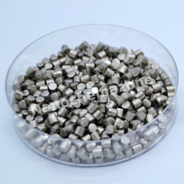
5N (99.999%) Aluminum (Al) Pellets Evaporation Materials

Price range: $145.00 through $1,318.00
Select options This product has multiple variants. The options may be chosen on the product page
Product 5N (99.999%) Aluminum (Al) Pellets Evaporation Materials
CAS No. 7429-90-5
Appearance Silvery, Metallic
Purity ≥99%,  ≥99.9%,  ≥95%(Other purities are also available)
APS N/A
Ingredient Al
Molecular Weight 26.98 g/mol
Melting Point 660°C
Boiling Point N/A
Density 2.7 g/cm³
Product Codes NCZ-100E
 

5N (99.999%) Silicon (P-type Si) Pieces (1-6mm) Evaporation Materials

Price range: $145.00 through $207.00
Select options This product has multiple variants. The options may be chosen on the product page
Product 5N (99.999%) Silicon (P-type Si) Pieces (1-6mm) Evaporation Materials
CAS No. 7440-21-3
Appearance Dark Gray with a Bluish Tinge, Semi-Metallic
Purity ≥99%,  ≥99.9%,  ≥95%(Other purities are also available)
APS 1-6mm (Size Can be customized),  Ask for other available size range.
Ingredient Si
Molecular Weight 28.0855 g/mol
Melting Point 1,410 °C
Boiling Point N/A
Density 2.32 g/cm3
Product Codes NCZ-146E

Zinc (Zn) Sputtering Targets, Purity: 99.95%, Size: 2”, Thickness: 0.125”

$145.00

Product 

Zinc (Zn) Sputtering Targets, Purity: 99.95%, Size: 2'', Thickness: 0.125''

CAS No.

7440‑66‑6

Appearance

Powder

Purity

≥99%,  ≥99.9%,  ≥95%

(Other purities are also available)

APS

Zn (black granules) (Size Can be customized), Ask for other available size ranges.

Ingredient

N/A

Molecular Weight

65.38 g/mol

Melting Point

419.5 °C

Boiling Point

 907 °C

Density

7.14 g/cm³

Product Codes

NCZ-1474K

5N (99.999%) Aluminum (Al) Pellets Evaporation Materials

Price range: $145.00 through $1,318.00
Select options This product has multiple variants. The options may be chosen on the product page
Product 5N (99.999%) Aluminum (Al) Pellets Evaporation Materials
CAS No. 7429-90-5
Appearance Silvery-white metallic solid
Purity ≥99%,  ≥99.9%,  ≥95%(Other purities are also available)
APS 1–5mm (Size Can be customized),  Ask for other available size range.
Ingredient Al
Molecular Weight 26.98 g/mol
Melting Point 660.3 °C
Boiling Point 2,470 °C
Density 2.70 g/cm³
Product Codes NCZ-192I
 

Silicon Dioxide (SiO2) Sputtering Targets, Fused Quartz, Purity: 99.995%, Size: 3”, Thickness: 0.125”

$145.00

Product 

Silicon Dioxide (SiO2) Sputtering Targets, Fused Quartz, Purity: 99.995%, Size: 3'', Thickness: 0.125''

CAS No.

7631-86-9

Appearance

Powder

Purity

≥99%,  ≥99.9%,  ≥95%

(Other purities are also available)

APS

N/A  (Size Can be customized), Ask for other available size ranges.

Ingredient

N/A

Molecular Weight

60.08 g/mol

Melting Point

~1710°C

Boiling Point

 ~2,950 °C

Density

~2.20 g/cm³

Product Codes

NCZ-1716K

Silver Indium (Ag-In) Alloy Nanopowder/Nanoparticles, Purity: 99.9%, Size: 40-100 nm

Price range: $145.28 through $2,088.46
Select options This product has multiple variants. The options may be chosen on the product page
Silver Indium (Ag-In) Alloy Nanopowder/Nanoparticles Purity: 99.9%, Size: 40-100 nm Technical Properties: Alloy Ratio (Ag-In) depends on customer needs Average Particle

Niobium Oxide (Nb2O5) Sputtering Targets, Purity: 99.5%, Size: 1”, Thickness: 0.250”

$146.00

Applications of Sputtering Targets;

Film deposition is accomplished using sputtering targets. A technique for sputtering thin films is called "deposition made by sputter targets," which entails eroding material from a "target" source onto a "substrate" like a silicon wafer. Etching of the target is done using semiconductor sputtering targets. When selectivity is not an issue and a high degree of etching anisotropy is required, sputter etching is the method of choice. By removing the target material through etching, sputter targets are also utilized for investigation. In secondary ion spectroscopy (SIMS), one example is when the target material is sputtered at a steady pace. Mass spectrometry is used to quantify the concentration and identity of spewed atoms as the target is sputtered.

The target material's composition may be ascertained and even very low concentrations of contaminants can be found with the aid of the sputtering target.

There is also an application area for sputtering targets in space. One type of space weathering that alters the chemical and physical characteristics of airless worlds like the Moon and asteroids is sputtering.

Niobium Aluminum Carbide (Nb4AlC3) MAX Phase Micron-Powder

Price range: $146.00 through $546.00
Select options This product has multiple variants. The options may be chosen on the product page
Product Niobium Aluminum Carbide (Nb4AlC3) MAX Phase Micron-Powder
CAS No. 1015077-01-6
Appearance Gray-black
Purity ≥99%,  ≥99.9%,  ≥95%(Other purities are also available)
APS  10–40µm (Size Can be customized),  Ask for other available size range.
Ingredient Nb4AlC3
Molecular Weight 434.63 g/mol
Melting Point N/A
Boiling Point N/A
Density 7.06 g/cm³
Product Codes NCZ-480I
 

Iron (Fe) Sputtering Targets, Purity: 99.99%, Size: 2”, Thickness: 0.125”

$146.00

Product 

Iron (Fe) Sputtering Targets, Purity: 99.99%, Size: 2'', Thickness: 0.125''

CAS No.

 7439-89-6

Appearance

Powder

Purity

≥99%,  ≥99.9%,  ≥95%

(Other purities are also available)

APS

 N/A (Size Can be customized), Ask for other available size ranges.

Ingredient

N/A

Molecular Weight

 55.85 g/mol

Melting Point

 1538 °C

Boiling Point

 2862 °C

Density

 7.87 g/cm³

Product Codes

NCZ-2187K

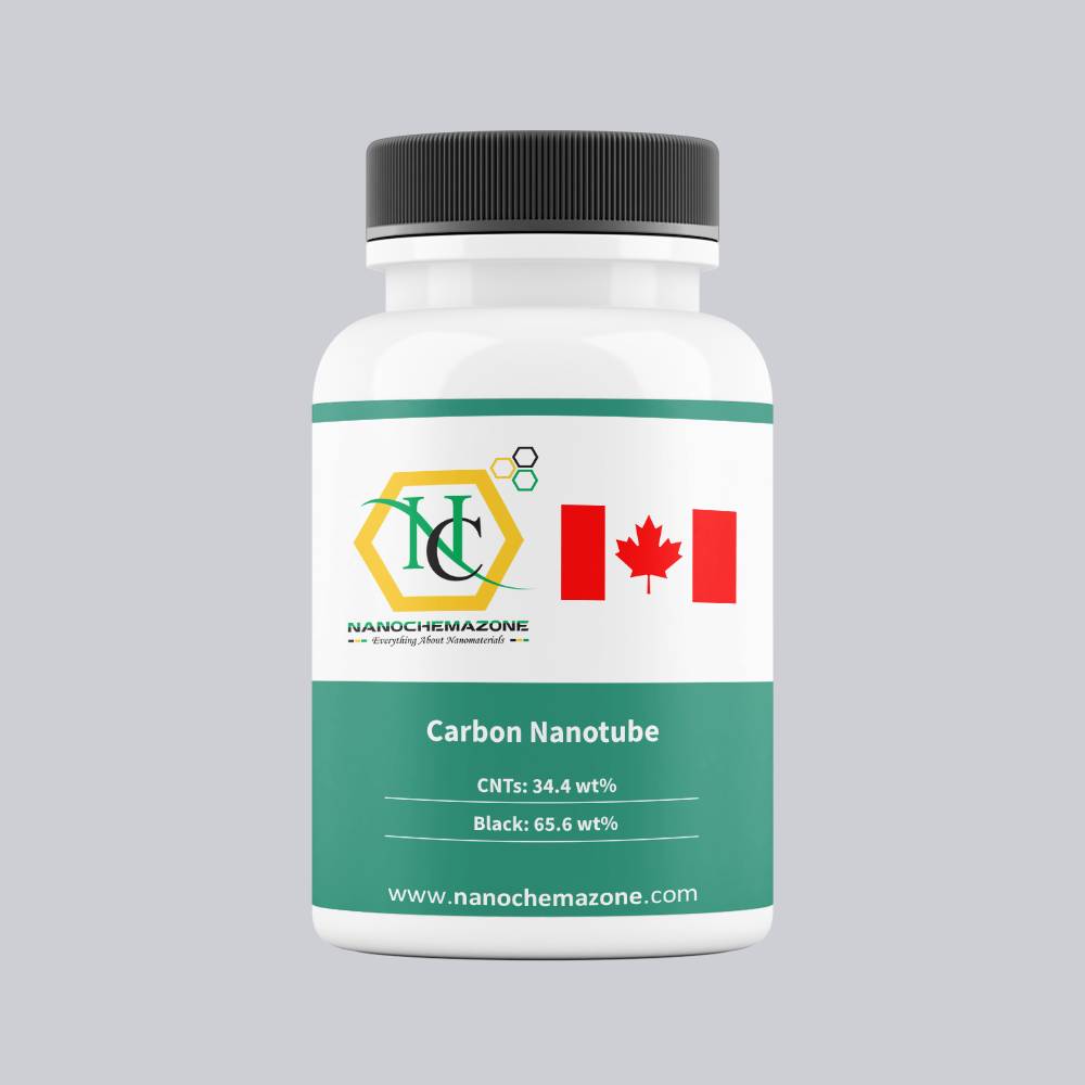
Carbon Nanotube-Carbon Black Prepared by Electrostatic Adsorption, CNTs: 34.4 wt%, Carbon Black: 65.6 wt%

Price range: $147.00 through $626.00
Select options This product has multiple variants. The options may be chosen on the product page
5 grams/134 € 25 grams/253 € 100 grams/568 €                                    
Please contact us for quotes on larger quantities !!!

Carbon Nanotube-Black Carbon Prepared by Electrostatic Adsorption

CNTs: 34.4 wt%, Carbon Black: 65.6 wt%

Technical Properties:

Carbon Nanotubes > 95 wt%
Purity >50
Outside Diameter (nm) 5.0-15.0
Inside Diameter (nm) 5.0-20.0
Length (μm) CVD
Color black
Super Conductive Black Carbon Nanoparticles 
Average Particle Size (nm) 50-100
Shape spherical
CNTs 33.3 wt%, Carbon Black 66.7 wt%
Specific Surface Area (m2/g) 560
Volume Resistivity (Ω.cm) <1
Volume Resistivity Content Relationship
CNTs Content wt%  0.00  25.00  33.30  60.00
Volume Resistivity (Ω·cm)  0.2150  0.1544  0.1332  0.1198

Applications:

Super conductive black carbon nanoparticles surface is usually negatively charged. Carbon nanotubes are treated with cationic surfactant (Cetyl trimethyl ammonium bromide). Carbon nanotubes and black carbon self assemble to form a uniform stable complex. The complex shows high strength and conductivity which makes it suitable for processing into conductive plastics, conductive sheets, and films.  

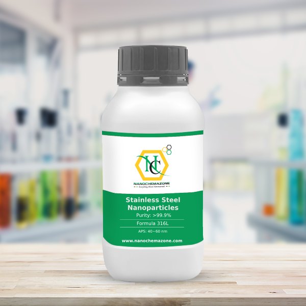
Stainless Steel Nanoparticles/ Nanopowder (40~60 nm)

Price range: $147.00 through $385.00
Select options This product has multiple variants. The options may be chosen on the product page
$147/25g
$385/100g

Product 

Stainless Steel Nanoparticles/ Nanopowder (40~60 nm)

CAS No.

65997-19-5

Appearance

Powder

Purity

≥99%,  ≥99.9%,  ≥95%

(Other purities are also available)

APS

(40~60 nm) (Size Can be customized), Ask for other available size ranges.

Ingredient

Iron (Fe) – ~65–70%, Chromium (Cr) – ~18–20%, Nickel (Ni) – ~8–10.5%, Manganese (Mn) – ≤2%, Silicon (Si) – ≤1%, Carbon (C) – ≤0.08%, Phosphorus (P) – ≤0.045%, Sulfur (S) – ≤0.03%

Molecular Weight

57.1 g/mol

Melting Point

1375–1400°C

Boiling Point

~2600–2900°C

Density

7.99 g/cm3

Product Codes

NCZ-1044K

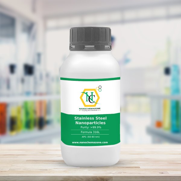
Stainless Steel Nanoparticles/ Nanopowder (60-80 nm)

Price range: $147.00 through $385.00
Select options This product has multiple variants. The options may be chosen on the product page
$147/25g
$385/100g

Product 

Stainless Steel Nanoparticles/ Nanopowder (60-80 nm)

CAS No.

65997-19-5

Appearance

Powder

Purity

≥99%,  ≥99.9%,  ≥95%

(Other purities are also available)

APS

(60-80 nm) (Size Can be customized), Ask for other available size ranges.

Ingredient

Iron (Fe) – ~65–70%, Chromium (Cr) – ~18–20%, Nickel (Ni) – ~8–10.5%, Manganese (Mn) – ≤2%, Silicon (Si) – ≤1%, Carbon (C) – ≤0.08%, Phosphorus (P) – ≤0.045%, Sulfur (S) – ≤0.03%

Molecular Weight

57.1 g/mol

Melting Point

1375–1400°C

Boiling Point

~2600–2900°C

Density

7.99 g/cm3

Product Codes

NCZ-1045K

Aluminum Sputtering Target

Price range: $147.00 through $741.00
Select options This product has multiple variants. The options may be chosen on the product page
Product Aluminum Sputtering Target
CAS No. 7429-90-5
Appearance Solid, metallic, silvery-white to gray
Purity ≥99%,  ≥99.9%,  ≥95% (Other purities are also available)
APS <100 µm (Size Can be customized),  Ask for other available size range.
Ingredient Al
Molecular Weight 26.98 g/mol
Melting Point 660.3 °C
Boiling Point 2,470 °C
Density 2.70 g/cm³
Product Codes NCZ-102H

Aluminum Silicon (AlSi) Sputtering Targets, Purity: 99.999%, Size: 2”, Thickness: 0.125”

$147.00

Product 

Aluminum Silicon (AlSi) Sputtering Targets, Purity: 99.999%, Size: 2'', Thickness: 0.125''

CAS No.

Aluminum: 7429-90-5 Silicon: 7440-21-3

Appearance

Powder

Purity

≥99%,  ≥99.9%,  ≥95%

(Other purities are also available)

APS

N/A (Size Can be customized), Ask for other available size ranges.

Ingredient

N/A

Molecular Weight

 Al: 26.98 g/mol Si: 28.09 g/mol

Melting Point

 ~577–660 °C (depends on Si content)

Boiling Point

~2519 °C (approx.)

Density

~2.6–2.7 g/cm³

Product Codes

NCZ-2517K

Copper Nickel Alloy Nanopowder, Cu55Ni45, APS: 50nm, Purity: 99.9%

Price range: $148.00 through $2,207.00
Select options This product has multiple variants. The options may be chosen on the product page
Copper Nickel Alloy Nanopowder, Cu55Ni45, APS: 50nm, Purity: 99.9% Performance characteristics Nano-copper-nickel alloy powder is prepared by gas phase CVD method, the alloy ratio can be adjusted appropriately, the purity is high, the particle size is small, the distribution is uniform, the surface area is large, easy to disperse, the industrial production is large, and it has good mechanical properties at room temperature and high temperature strength. It has high corrosion resistance, good wear resistance, easy processing, and non-magnetic. It is a good structural material for manufacturing traveling wave tubes and other electron tubes, and can also be used as a structural material for aero engines. Product parameter
APS 50 nm
Purity 99.9 %
BET Surface Area 28.84 m2/g
Theoritical density 8.800 g/cm3
Bulk density 0.949 g/cm3
Melting Point 900 °C
Boiling Point 1500 °C
Shape Spherical
Color Black Powder
Manufacturing Method CVD

Styrene-Butadiene Rubber (SBR) Binder for Li-ion Battery Anode Materials

Price range: $148.00 through $247.00
Select options This product has multiple variants. The options may be chosen on the product page
500 ml/148 € 1000 ml/247 € Please contact us for quotes on larger quantities !!! Styrene-Butadiene Rubber (SBR) Binder for Li-ion Battery Anode

Titanium Foam for Battery and Supercapacitor Research, Purity: 99+%, Size: 100 mm x100 mm x 2.8mm

Price range: $148.00 through $613.00
Select options This product has multiple variants. The options may be chosen on the product page
APPLICATIONS
  • Titanium foam is used as a substrate for battery and supercapacitor applications.
  • It is used as a substrate for in-situ growth of hierarchical electrode material which is beneficial from its porous structure.
  • Also used in the pharmaceutical industry, water treatment industry, food industry, biological engineering, chemical industry, petrochemical industry, metallurgical industry, and gas purification field.

Molybdenum (Mo) Sputtering Targets, Purity: 99.95%, Size: 2”, Thickness: 0.125”

$148.00

Applications of Sputtering Targets;

Film deposition is accomplished using sputtering targets. A technique for sputtering thin films is called "deposition made by sputter targets," which entails eroding material from a "target" source onto a "substrate" like a silicon wafer. Etching of the target is done using semiconductor sputtering targets. When selectivity is not an issue and a high degree of etching anisotropy is required, sputter etching is the method of choice. By removing the target material through etching, sputter targets are also utilized for investigation. In secondary ion spectroscopy (SIMS), one example is when the target material is sputtered at a steady pace. Mass spectrometry is used to quantify the concentration and identity of spewed atoms as the target is sputtered.

By helping of the sputtering target, the composition of the target material may be evaluated and even extremely tiny amounts of contaminants are recognized.

There is also an application area for sputtering targets in space. One type of space weathering that alters the chemical and physical characteristics of airless worlds like the Moon and asteroids is sputtering.

Tungsten Titanium (TiW) Sputtering Targets, Purity: 99.995%, Size: 1”, Thickness: 0.250”

$148.00

Applications of Sputtering Targets;

Film deposition is accomplished using sputtering targets. A technique for sputtering thin films is called "deposition made by sputter targets," which entails eroding material from a "target" source onto a "substrate" like a silicon wafer. Etching of the target is done using semiconductor sputtering targets. When selectivity is not an issue and a high degree of etching anisotropy is required, sputter etching is the method of choice. By removing the target material through etching, sputter targets are also utilized for investigation. In secondary ion spectroscopy (SIMS), one example is when the target material is sputtered at a steady pace. Mass spectrometry is used to quantify the concentration and identity of spewed atoms as the target is sputtered.

The target material's composition may be ascertained and even very low concentrations of contaminants can be found with the aid of the sputtering target.

There is also an application area for sputtering targets in space. One type of space weathering that alters the chemical and physical characteristics of airless worlds like the Moon and asteroids is sputtering.

Nickel Vanadium Sputtering Target NiV

Price range: $148.00 through $421.00
Select options This product has multiple variants. The options may be chosen on the product page
Product Nickel Vanadium Sputtering Target NiV
CAS No. 685830-44-8
Appearance Metallic, silver white sputtering target
Purity ≥99%,  ≥99.9%,  ≥95%(Other purities are also available)
APS 5–20µm (Size Can be customized),  Ask for other available size range.
Ingredient NiV
Molecular Weight 109.63 g/mol
Melting Point 1875 °C
Boiling Point 3407 °C
Density N/A
Product Codes NCZ-133H
 

5N (99.999%) Perovskite Grade Lead (II) Bromide (PbBr2), 5g

$148.00
Product 5N (99.999%) Perovskite Grade Lead (II) Bromide (PbBr2), 5g
CAS No. 10031-22-8
Appearance White 
Purity ≥99%,  ≥99.9%,  ≥95%(Other purities are also available)
APS 100nm-10µm (Size Can be customized), Ask for other available size range.
Ingredient PbBr2
Molecular Weight 367.01 g/mol
Melting Point 371 °C
Boiling Point 892 °C
Density 6.66 g/cm³
Product Codes NCZ-101I
 

Gallium Arsenide (GaAs) Wafers, Size: 2”, Thickness: 350±25 μm, Single Side Polished, EPI-ready

Price range: $149.00 through $2,875.00
Select options This product has multiple variants. The options may be chosen on the product page
1 piece/135  5 pieces/635  25 pieces/2590  Please contact us for quotes on larger quantities !!!

Gallium Arsenide (GaAs) Wafer

Size: 2”, Thickness: 350±25 μm, Single Side Polished

Technical Properties:

Quality  GaAs
Materials  GaAs
Size (inch)  2”
Thickness (μm)  350± 25
Polished  Single Side
Dopant  Silicon ( N type )
Orientation  (100)15 deg off toward <111>A±0.5
Resistivity   (1.2—9.9) E-3
Mobility  1000-3000
EPD  ≤3000
Growth method  VGF
OF Length  17±1
IF Length   7±1

Fields of Application for Gallium Arsenide (GaAs)

Gallium arsenide (GaAs) is a compound of the elements gallium and arsenic. Gallium arsenide (GaAs) is a semiconductor compound. Gallium arsenide (GaAs)  has a high electron velocity and high saturated electron mobility. This makes gallium arsenide (GaAs) components are useful in fast electronic switching applications and at ultra-high radio frequencies. In 1907, the British discovered infrared emmission from gallium arsenide. This was called electroluminescence. Also, gallium arsenide (GaAs) was used as a solar cells in space for the Venera 3 mission in 1965, which is the first known operational use of gallium arsenide (GaAs). Vertical gradient freeze is the most common method to produce GaAs wafers. Mainly used for circuits, electronics and solar cell applications. Carbon, silicon, tellurium and zinc are some of the dopants that are used to modify the characteristics and electrical properties of gallium arsenide wafers. Wafer flatness and surface purity are ensured by highest quality standards. Boron concentration of gallium arsenide wafers highly depend on the production method. Gallium arsenide wafers with adequate electrical resistancy prevent high current induction in the circuit. Mobility of GaAs wafers can be tailored with different doping levels.
  • Gallium arsenide (GaAs) is used in laser diodes.
  • Gallium arsenide (GaAs) is used in solar cells.
  • Gallium arsenide (GaAs) is used in optical windows.
  • Gallium arsenide (GaAs) is used in monolithic microwave integrated circuits.
  • Gallium arsenide (GaAs) is used in microwave frequency integrated circuits.
  • Gallium arsenide (GaAs) is used in infrared light-emitting diodes.
  • Gallium arsenide (GaAs) is useful in barometers.
  • Gallium arsenide (GaAs) is useful in pharmaceuticals and nuclear medicine tests.
  • Gallium arsenide (GaAs) is useful in high temperature thermometers.

Carbon Nanotube-Carbon Black Prepared by Electrostatic Adsorption, CNTs: 34.4 wt%, Carbon Black: 65.6 wt%

Price range: $149.00 through $624.00
Select options This product has multiple variants. The options may be chosen on the product page

Applications:

The surface of superconductive black carbon nanoparticles is usually negatively charged. A cationic surfactant (Cetyl trimethyl ammonium bromide) is used to treat carbon nanotubes. Carbon nanotubes and black carbon self-assemble to form a stable complex that is uniform. Because of its high strength and conductivity, the complex is suitable for processing into conductive plastics, conductive sheets, and conductive films.

Carbon Nanotube-Carbon Black Prepared by Electrostatic Adsorption, CNTs: 34.4 wt%, Carbon Black: 65.6 wt%

Price range: $149.00 through $624.00
Select options This product has multiple variants. The options may be chosen on the product page
Carbon Nanotube-Black Carbon Prepared by Electrostatic Adsorption CNTs: 34.4 wt%, Carbon Black: 65.6 wt% Technical Properties: Carbon Nanotubes > 95

Yttrium (Y) Sputtering Targets, Purity: 99.9%, Size: 1”, Thickness: 0.125”

$149.00

Applications of Sputtering Targets;

  • Sputtering targets is used for film deposition. The deposition made by sputter targets is a method of depositing thin films by sputtering that involves eroding material from a "target" source onto a "substrate" such as  a silicon wafer.
  • Semiconductor sputtering targets is used to etch the target. Sputter etching is chosen in cases where a high degree of etching anisotropy is needed and selectivity is not a concern.
  • Sputter targets is also used for analysis by etching away the target material.
One of the example occurs in secondary ion spectroscopy (SIMS), where the target sample is sputtered at a constant rate. As the target is sputtered, the concentration and identity of sputtered atoms are measured using mass spectrometry. By helping of the sputtering target, the composition of the target material can be determined and even extremely low concentrations of impurities are detected. Sputtering target has also application area in space. Sputtering is one of the forms of space weathering, a process that changes the physical and chemical properties of airless bodies, such as asteroids and the Moon.

Copper (Cu) Sputtering Targets, Purity: 99.999%, Size: 2”, Thickness: 0.250”

$149.00

Applications of Sputtering Targets;

Film deposition is accomplished using sputtering targets. A technique for sputtering thin films is called "deposition made by sputter targets," which entails eroding material from a "target" source onto a "substrate" like a silicon wafer. Etching of the target is done using semiconductor sputtering targets. When selectivity is not an issue and a high degree of etching anisotropy is required, sputter etching is the method of choice. By removing the target material through etching, sputter targets are also utilized for investigation. In secondary ion spectroscopy (SIMS), one example is when the target material is sputtered at a steady pace. Mass spectrometry is used to quantify the concentration and identity of spewed atoms as the target is sputtered.

The target material's composition may be ascertained and even very low concentrations of contaminants can be found with the aid of the sputtering target.

There is also an application area for sputtering targets in space. One type of space weathering that alters the chemical and physical characteristics of airless worlds like the Moon and asteroids is sputtering.

Nickel Sputtering Target Ni

Price range: $149.00 through $706.00
Select options This product has multiple variants. The options may be chosen on the product page
Product Nickel Sputtering Target Ni
CAS No. 7440-02-0
Appearance Silvery-white lustrous metals
Purity ≥99%,  ≥99.9%,  ≥95%(Other purities are also available)
APS N/A
Ingredient Ni
Molecular Weight 58.69 g/mol
Melting Point 1453.0 °C
Boiling Point 2732.0 °C 
Density N/A
Product Codes NCZ-132H

4N (99.99%) Zinc (Zn) Pellets Evaporation Materials

Price range: $149.00 through $989.00
Select options This product has multiple variants. The options may be chosen on the product page
Product 4N (99.99%) Zinc (Zn) Pellets Evaporation Materials
CAS No. 7440-66-6
Appearance Bluish Pale Gray, Metallic
Purity ≥99%,  ≥99.9%,  ≥95%(Other purities are also available)
APS N/A
Ingredient Zn
Molecular Weight 65.38 g/mol
Melting Point N/A
Boiling Point N/A
Density 7.14 g/cm³
Product Codes NCZ-177I

Magnesium (Mg) Sputtering Targets, Purity: 99.98%, Size: 1”, Thickness: 0.125”

$149.00

Product 

Magnesium (Mg) Sputtering Targets, Purity: 99.98%, Size: 1'', Thickness: 0.125''

CAS No.

7439-95-4

Appearance

Powder

Purity

≥99%,  ≥99.9%,  ≥95%

(Other purities are also available)

APS

 N/A (Size Can be customized), Ask for other available size ranges.

Ingredient

N/A

Molecular Weight

 24.305 g/mol

Melting Point

 650 °C

Boiling Point

 1,090 °C

Density

1.738 g/cm³

Product Codes

NCZ-2006K

Erbium Oxide (Er2O3) Sputtering Targets, Purity: 99.99%, Size: 1”, Thickness: 0.125”

$150.00
Select options This product has multiple variants. The options may be chosen on the product page

Applications of Sputtering Targets;

  • Sputtering targets is used for film deposition. The deposition made by sputter targets is a method of depositing thin films by sputtering that involves eroding material from a "target" source onto a "substrate" such as  a silicon wafer.
  • Semiconductor sputtering targets is used to etch the target. Sputter etching is chosen in cases where a high degree of etching anisotropy is needed and selectivity is not a concern.
  • Sputter targets is also used for analysis by etching away the target material.
One of the example occurs in secondary ion spectroscopy (SIMS), where the target sample is sputtered at a constant rate. As the target is sputtered, the concentration and identity of sputtered atoms are measured using mass spectrometry. By helping of the sputtering target, the composition of the target material can be determined and even extremely low concentrations of impurities are detected. Sputtering target has also application area in space. Sputtering is one of the forms of space weathering, a process that changes the physical and chemical properties of airless bodies, such as asteroids and the Moon. Erbium oxide with a chemical formula of Er2Ois an oxide of erbium metal. The applications of erbium oxide are varied due to their electrical, optical and photoluminescence properties. Nanoscale materials doped with Er+3 are of much interest because they have special particle-size-dependent optical and electrical properties. Erbium oxide doped nanoparticle materials can be dispersed in glass or plastic for display purposes, such as display monitors. The spectroscopy of Er+3 electronic transitions in host crystals lattices of nanoparticles combined with ultrasonically formed geometries in aqueous solution of carbon nanotubes is of great interest for synthesis of photoluminescence nanoparticles in ‘green’ chemistry. Erbium oxide is among the most important rare earth metals used in biomedicine. Erbium oxides are also used as gate dielectrics in semiconductor devices since it has a high dielectric constant (10-14) and a large band gap. Erbium is sometimes used as a coloring for glasses and erbium oxide can also be used as a burnable neutron poison for nuclear fuel. Erbium oxide films obtained by sputtering can be used for their photoluminescence effect.