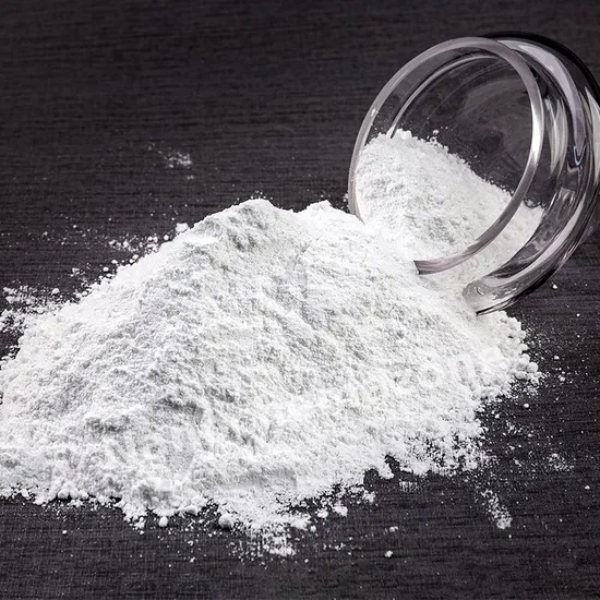
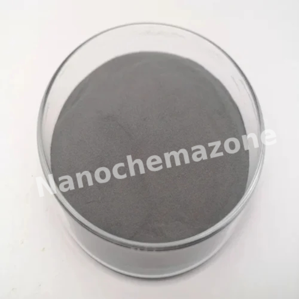
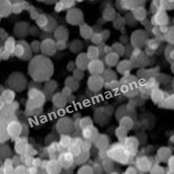
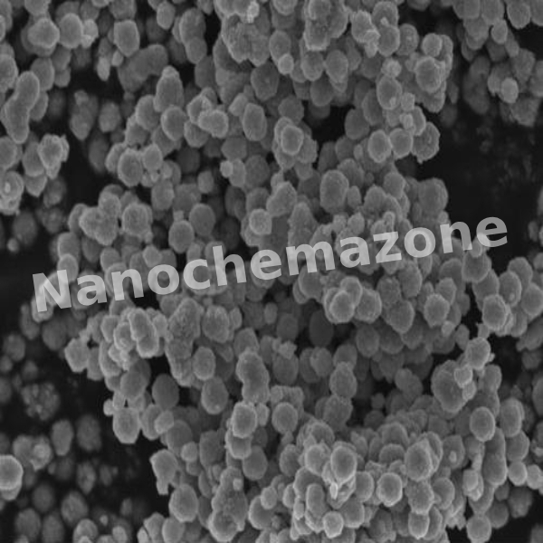
40nm Monoclinic Zirconium Dioxide ZrO2 Nanoparticles, >99.9% High Purity

Price range: $132.00 through $1,859.00
Select options This product has multiple variants. The options may be chosen on the product page
Product 40nm Monoclinic Zirconium Dioxide ZrO2 Nanoparticles, >99.9% High Purity
CAS No. 1314-23-4
Appearance White or off-white
Purity ≥99%,  ≥99.9%,  ≥95%(Other purities are also available)
APS 40nm (Size Can be customized),  Ask for other available size range.
Ingredient ZrO₂
Molecular Weight 123.22 g/mol
Melting Point 2,715 °C
Boiling Point 4,300 °C
Density 5.68 g/cm³
Product Codes NCZ-164I

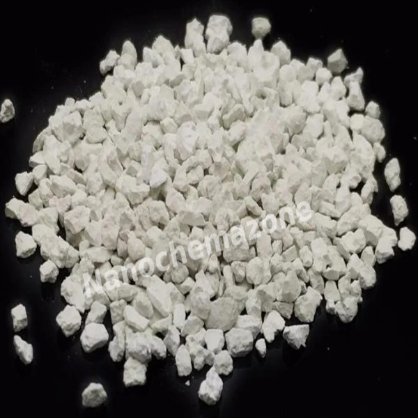
4N (99.99%) Aluminum Fluoride (AlF3) Pieces (1-10mm) Evaporation Materials, 250g

Price range: $132.00 through $1,859.00
Select options This product has multiple variants. The options may be chosen on the product page
Product 4N (99.99%) Aluminum Fluoride (AlF3) Pieces (1-10mm) Evaporation Materials, 250g
CAS No. 7784-18-1
Appearance White solid
Purity ≥99%,  ≥99.9%,  ≥95%(Other purities are also available)
APS 1-10mm (Size Can be customized),  Ask for other available size range.
Ingredient AlF3
Molecular Weight 123.22 g/mol
Melting Point N/A
Boiling Point N/A
Density 5.68 g/cm³
Product Codes NCZ-165I
 

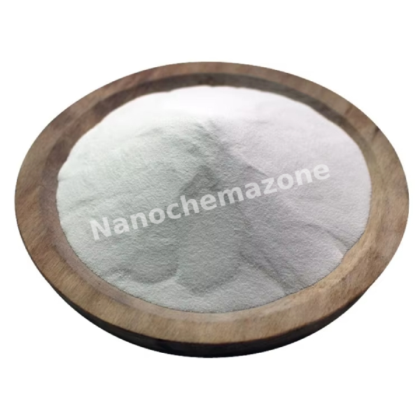
50nm Monoclinic Zirconium Dioxide ZrO2 Nanoparticles, >99.9% High Purity

Price range: $132.00 through $1,859.00
Select options This product has multiple variants. The options may be chosen on the product page
Product 50nm Monoclinic Zirconium Dioxide ZrO2 Nanoparticles, >99.9% High Purity
CAS No. 1314-23-4
Appearance White
Purity ≥99%,  ≥99.9%,  ≥95%(Other purities are also available)
APS 50nm (Size Can be customized),  Ask for other available size range.
Ingredient ZrO2
Molecular Weight 123.22 g/mol
Melting Point 2,715 °C
Boiling Point N/A
Density 5.68 g/cm³
Product Codes NCZ-189I

80nm Monoclinic Zirconium Dioxide ZrO2 Nanoparticles, >99.9% High Purity

Price range: $132.00 through $1,859.00
Select options This product has multiple variants. The options may be chosen on the product page
Product 80nm Monoclinic Zirconium Dioxide ZrO2 Nanoparticles, >99.9% High Purity
CAS No. 1314-23-4
Appearance Fine white
Purity ≥99%,  ≥99.9%,  ≥95%(Other purities are also available)
APS 80nm (Size Can be customized),  Ask for other available size range.
Ingredient ZrO2
Molecular Weight 123.22 g/mol
Melting Point N/A
Boiling Point N/A
Density 5.7–5.9 g/cm³
Product Codes NCZ-204I

Aluminum Fluoride (AlF3) Powder, 99%, 1kg

$132.00
Select options This product has multiple variants. The options may be chosen on the product page
Product Aluminum Fluoride (AlF3) Powder, 99%, 1kg
CAS No. 7784-18-1
Appearance White to off-white crystalline
Purity ≥99%,  ≥99.9%,  ≥95%(Other purities are also available)
APS 10–50µm (Size Can be customized),  Ask for other available size range.
Ingredient AlF3
Molecular Weight 83.98 g/mol
Melting Point 1,290 °C
Boiling Point N/A
Density 3.10 g/cm³
Product Codes NCZ-281I

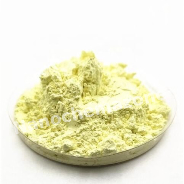
Bismuth (III) Oxide (Bi2O3) Powder, 99.999% (5N) (Metal Basis)

$132.00
Select options This product has multiple variants. The options may be chosen on the product page
Product Bismuth (III) Oxide (Bi2O3) Powder, 99.999% (5N) (Metal Basis)
CAS No. 1304-76-3
Appearance Bright yellow crystalline
Purity ≥99%,  ≥99.9%,  ≥95%(Other purities are also available)
APS 1-5µm (Size Can be customized),  Ask for other available size range.
Ingredient Bi2O3
Molecular Weight 465.96 g/mol
Melting Point N/A
Boiling Point N/A
Density 8.9 g/cm³
Product Codes NCZ-299I

Boron, B, 99.9% Powder, 100g

$132.00
Select options This product has multiple variants. The options may be chosen on the product page
Product Boron, B, 99.9% Powder, 100g
CAS No. 7440-42-8
Appearance Brownish black fine
Purity ≥99%,  ≥99.9%,  ≥95%(Other purities are also available)
APS 1-10µm (Size Can be customized),  Ask for other available size range.
Ingredient B
Molecular Weight 10.81 g/mol
Melting Point N/A
Boiling Point N/A
Density 2.34 g/cm³
Product Codes NCZ-300I
 

Aluminum (Al) Sputtering Targets, Purity: 99.999%, Size: 1”, Thickness: 0.125”

$132.00

Product 

Aluminum (Al) Sputtering Targets, Purity: 99.999%, Size: 1'', Thickness: 0.125''

CAS No.

 7429-90-5

Appearance

Powder

Purity

≥99%,  ≥99.9%,  ≥95%

(Other purities are also available)

APS

N/A (Size Can be customized), Ask for other available size ranges.

Ingredient

N/A

Molecular Weight

 26.98 g/mol

Melting Point

 660.3 °C

Boiling Point

 2519 °C

Density

 2.70 g/cm³

Product Codes

NCZ-2583K

Silicon Dioxide (SiO2) Sputtering Targets, Fused Quartz, Purity: 99.995%, Size: 3”, Thickness: 0.250”

$133.00

Applications of Sputtering Targets;

Film deposition is accomplished using sputtering targets. A technique for sputtering thin films is called "deposition made by sputter targets," which entails eroding material from a "target" source onto a "substrate" like a silicon wafer. Etching of the target is done using semiconductor sputtering targets. When selectivity is not an issue and a high degree of etching anisotropy is required, sputter etching is the method of choice. By removing the target material through etching, sputter targets are also utilized for investigation. In secondary ion spectroscopy (SIMS), one example is when the target material is sputtered at a steady pace. Mass spectrometry is used to quantify the concentration and identity of spewed atoms as the target is sputtered.

The target material's composition may be ascertained and even very low concentrations of contaminants can be found with the aid of the sputtering target.

There is also an application area for sputtering targets in space. One type of space weathering that alters the chemical and physical characteristics of airless worlds like the Moon and asteroids is sputtering.

Iron Nanoparticles/ Nanopowder ( Fe, 99.7%, 40~60nm)

Price range: $133.00 through $2,479.00
Select options This product has multiple variants. The options may be chosen on the product page
$133/25g
$370/100g
$1375/500g
$2479/kg

Product 

Iron Nanoparticles/ Nanopowder ( Fe, 99.7%, 40~60nm)

CAS No.

7439-89-6

Appearance

Powder

Purity

≥99%,  ≥99.9%,  ≥95%

(Other purities are also available)

APS

300 nm (Size Can be customized), Ask for other available size ranges.

Ingredient

AlN

Molecular Weight

63.55 g/mol

Melting Point

1084.62 °C

Boiling Point

2562 °C

Density

8.96 g/cm³

Product Codes

NCZ-1041K

Cerium Oxide Nanoparticles / Nanopowder doped with Gadolinium

Price range: $133.00 through $337.00
Select options This product has multiple variants. The options may be chosen on the product page
$133/25g
$337/100g

Product 

Cerium Oxide Nanoparticles / Nanopowder doped with Gadolinium

CAS No.

N/A

Appearance

Powder

Purity

≥99%,  ≥99.9%,  ≥95%

(Other purities are also available)

APS

<100 nm(Size Can be customized), Ask for other available size ranges.

Ingredient

N/A

Molecular Weight

172.11 g/mol

Melting Point

 ~2,400 °C

Boiling Point

~3,500 °C

Density

~7.13 g/cm³

Product Codes

NCZ-1121K

Cerium Oxide doped with Gadolinium Nanoparticles (10mol%Gd2O3+90mol%CeO2, 99.9%, <100 nm)

Price range: $133.00 through $337.00
Select options This product has multiple variants. The options may be chosen on the product page
$133/25g $337/100g
Product Cerium Oxide doped with Gadolinium Nanoparticles (10mol%Gd2O3+90mol%CeO2, 99.9%, <100 nm)
CAS No. 1306-38-3
Appearance White or pale yellow powder
Purity ≥99%,  ≥99.9%,  ≥95%(Other purities are also available)
APS 100 nm (Size Can be customized),  Ask for other available size range.
Ingredient CeO2
Molecular Weight 177.38 g/mol
Melting Point 2400°C
Boiling Point N/A
Density 7.2g/cm³
Product Codes NCZ-105R

Vanadium (V) Sputtering Target

Price range: $133.00 through $547.00
Select options This product has multiple variants. The options may be chosen on the product page

Product 

Vanadium (V) Sputtering Target

CAS No.

7440-62-2

Appearance

Powder

Purity

≥99%,  ≥99.9%,  ≥95%

(Other purities are also available)

APS

 NA (Size Can be customized), Ask for other available size ranges.

Ingredient

N/A

Molecular Weight

50.9415 g/mol

Melting Point

1,910 °C

Boiling Point

3,407 °C

Density

 6.11 g/cm³

Product Codes

NCZ-1308K

Copper (Cu) Sputtering Targets, Purity: 99.999%, Size: 2”, Thickness: 0.125”

$134.00

Product 

Copper (Cu) Sputtering Targets, Purity: 99.999%, Size: 2'', Thickness: 0.125''

CAS No.

7440-50-8

Appearance

Powder

Purity

≥99%,  ≥99.9%,  ≥95%

(Other purities are also available)

APS

 N/A (Size Can be customized), Ask for other available size ranges.

Ingredient

N/A

Molecular Weight

63.55 g/mol

Melting Point

1,084 °C

Boiling Point

 2,562 °C

Density

8.96 g/cm³

Product Codes

NCZ-2269K

Scandium (Sc) Micron Powder, Purity: 99.9 %, Particle Size: 200 mesh

Price range: $135.00 through $3,687.00
Select options This product has multiple variants. The options may be chosen on the product page

Applications:

Scandium is one of the transition metals. Scandium is oxidized in air giving yellow or pinkish color. Scandium is found in over 800 mineral species. It can be found in concentrated amounts in the minerals euxenite, gadolinite and thortveitite.Scandium is mainly applied in aluminum scandium alloys. Scandium's light weight makes Scandium  suitable for minor aerospace industry components. 

Bismuth (III) Sulfide (Bi2S3) Nanopowder/Nanoparticles, Purity: 99.9+%, Size: 500 nm

$136.00
Select options This product has multiple variants. The options may be chosen on the product page
25 grams/120 €
Please contact us for quotes on larger quantities!

Bismuth (III) Sulfide (Bi2S3) Nanopowder/Nanoparticles

Purity: 99.9+%, Size: 500 nm

Praseodymium (Pr) Sputtering Targets, Purity: 99.9%, Size: 2”, Thickness: 0.250”

$136.00

Applications of Sputtering Targets;

  • Sputtering targets is used for film deposition. The deposition made by sputter targets is a method of depositing thin films by sputtering that involves eroding material from a "target" source onto a "substrate" such as  a silicon wafer.
  • Semiconductor sputtering targets is used to etch the target. Sputter etching is chosen in cases where a high degree of etching anisotropy is needed and selectivity is not a concern.
  • Sputter targets is also used for analysis by etching away the target material.
One of the example occurs in secondary ion spectroscopy (SIMS), where the target sample is sputtered at a constant rate. As the target is sputtered, the concentration and identity of sputtered atoms are measured using mass spectrometry. By helping of the sputtering target, the composition of the target material can be determined and even extremely low concentrations of impurities are detected. Sputtering target has also application area in space. Sputtering is one of the forms of space weathering, a process that changes the physical and chemical properties of airless bodies, such as asteroids and the Moon.

Iron (Fe) Sputtering Targets, Purity: 99.95%, Size: 3”, Thickness: 0.125”

$136.00

Applications of Sputtering Targets;

Film deposition is accomplished using sputtering targets. A technique for sputtering thin films is called "deposition made by sputter targets," which entails eroding material from a "target" source onto a "substrate" like a silicon wafer. Etching of the target is done using semiconductor sputtering targets. When selectivity is not an issue and a high degree of etching anisotropy is required, sputter etching is the method of choice. By removing the target material through etching, sputter targets are also utilized for investigation. In secondary ion spectroscopy (SIMS), one example is when the target material is sputtered at a steady pace. Mass spectrometry is used to quantify the concentration and identity of spewed atoms as the target is sputtered.

Nickel (Ni) Sputtering Targets, Purity: 99.99%, Size: 1”, Thickness: 0.125”

$136.00

Applications of Sputtering Targets;

Film deposition is accomplished using sputtering targets. A technique for sputtering thin films is called "deposition made by sputter targets," which entails eroding material from a "target" source onto a "substrate" like a silicon wafer. Etching of the target is done using semiconductor sputtering targets. When selectivity is not an issue and a high degree of etching anisotropy is required, sputter etching is the method of choice. By removing the target material through etching, sputter targets are also utilized for investigation. In secondary ion spectroscopy (SIMS), one example is when the target material is sputtered at a steady pace. Mass spectrometry is used to quantify the concentration and identity of spewed atoms as the target is sputtered.

By helping of the sputtering target, the composition of the target material may be evaluated and even extremely tiny amounts of contaminants are recognized.

There is also an application area for sputtering targets in space. One type of space weathering that alters the chemical and physical characteristics of airless worlds like the Moon and asteroids is sputtering.

Praseodymium (Pr) Sputtering Targets, Purity: 99.9%, Size: 2”, Thickness: 0.250”

$136.00

Applications of Sputtering Targets;

Film deposition is accomplished using sputtering targets. A technique for sputtering thin films is called "deposition made by sputter targets," which entails eroding material from a "target" source onto a "substrate" like a silicon wafer. Etching of the target is done using semiconductor sputtering targets. When selectivity is not an issue and a high degree of etching anisotropy is required, sputter etching is the method of choice. By removing the target material through etching, sputter targets are also utilized for investigation. In secondary ion spectroscopy (SIMS), one example is when the target material is sputtered at a steady pace. Mass spectrometry is used to quantify the concentration and identity of spewed atoms as the target is sputtered.

The target material's composition may be ascertained and even very low concentrations of contaminants can be found with the aid of the sputtering target.

There is also an application area for sputtering targets in space. One type of space weathering that alters the chemical and physical characteristics of airless worlds like the Moon and asteroids is sputtering.

Zirconium Carbide Nanoparticles/ Nanopowder ( ZrC, 97+%, 60nm)

Price range: $136.00 through $467.00
Select options This product has multiple variants. The options may be chosen on the product page
$136/25g
$467/100g

Product 

Zirconium Carbide Nanoparticles/ Nanopowder ( ZrC, 97+%, 60nm)

CAS No.

12070-14-3

Appearance

Powder

Purity

≥99%,  ≥99.9%,  ≥95%

(Other purities are also available)

APS

60nm (Size Can be customized), Ask for other available size ranges.

Ingredient

N/A

Molecular Weight

103.23 g/mol

Melting Point

~3,532 °C

Boiling Point

~5,100 °C

Density

 ~6.73 g/cm³

Product Codes

NCZ-1228K

Single Walled Nanotubes (SWNTs 95%)

Price range: $136.00 through $467.00
Select options This product has multiple variants. The options may be chosen on the product page
$205/1g
$725/5g

Product 

Single Walled Nanotubes (SWNTs 95%)

CAS No.

7727-54-0

Appearance

Powder

Purity

≥99%,  ≥99.9%,  ≥95%

(Other purities are also available)

APS

 1-2 nm (Size Can be customized), Ask for other available size ranges.

Ingredient

N/A

Molecular Weight

 228.20 g/mol

Melting Point

 120 °C

Boiling Point

N/A

Density

1.98 g/cm³

Product Codes

NCZ-1237K

High Purity Short MWNTs 98+%, <8nm

Price range: $136.00 through $467.00
Select options This product has multiple variants. The options may be chosen on the product page
$120/5g
$320/25g
$615/100g

Product 

High Purity Short MWNTs 98+%, <8nm

CAS No.

7727-54-0

Appearance

Powder

Purity

≥99%,  ≥99.9%,  ≥95%

(Other purities are also available)

APS

<8nm (Size Can be customized), Ask for other available size ranges.

Ingredient

N/A

Molecular Weight

228.20 g/mol

Melting Point

 120 °C

Boiling Point

N/A

Density

1.98 g/cm³

Product Codes

NCZ-1241K

Double Walled Carbon Nanotubes ( DWNTs, 60%, 2~4nm)

Price range: $136.00 through $467.00
Select options This product has multiple variants. The options may be chosen on the product page
$90/1g
$313/5g

Product 

Double Walled Carbon Nanotubes ( DWNTs, 60%, 2~4nm)

CAS No.

7727-54-0

Appearance

Powder

Purity

≥99%,  ≥99.9%,  ≥95%

(Other purities are also available)

APS

2~4nm (Size Can be customized), Ask for other available size ranges.

Ingredient

N/A

Molecular Weight

228.20 g/mol

Melting Point

 120 °C

Boiling Point

N/A

Density

1.98 g/cm³

Product Codes

NCZ-1246K

99.995% 4N5 Indium Foil (50x50x0.5 mm) for Heat Sink and Solid State Battery

$136.00
Select options This product has multiple variants. The options may be chosen on the product page
Product 99.995% 4N5 Indium Foil (50x50x0.5 mm) for Heat Sink and Solid State Battery
CAS No. 7440-74-6
Appearance Silvery-white, soft metallic sheet
Purity ≥99%,  ≥99.9%,  ≥95%(Other purities are also available)
APS 10–100µm (Size Can be customized),  Ask for other available size range.
Ingredient In
Molecular Weight 138.205 g/mol
Melting Point 156.6 °C
Boiling Point N/A
Density 7.31 g/cm³
Product Codes NCZ-255I

Graphene Water Dispersion, Purity: 99.5%, Black Liquid, Graphene: 1,0 wt%

Price range: $137.00 through $2,603.00
Select options This product has multiple variants. The options may be chosen on the product page
30 ml/125 € 60 ml/224 €                          120 ml/395 €                        500 ml/1280 €                   1000 ml/2360 € Please contact us for quotes on larger quantities !!!

Graphene Water Dispersion

Purity: 99.5%, Black Liquid, Graphene: 1,0 wt%

Graphene water dispersion raises environmentally safe handing of graphene for coating, composite, and other material applications. Graphene water dispersion is obtained by bath sonication of natural graphite flakes in water mixtures. Graphene water dispersion has outperformed commercial nano graphite at much lower loadings. Nanografi supplies Graphene Water Dispersion with high quantity and more types for different applications.

Technical Properties:

Graphene Purity (%) 99,5
Graphene Thickness (nm) 0,6-1,2 (single layer)
Diameter (µm) 2,0-12,0
Appearance Black Liquid
Concentration  (wt%) 1,0 (can be easily diluted)
Specific Surface Area (m2/g) 600-1200
Elemental Analysis C O
99,6 <0,4
 

Polyhydroxylated Fullerene (Fullerenols)/ C60, (-OH) Functionalized, Dispersed in Water, 250 ppm Dry powder

Price range: $137.00 through $2,488.00
Select options This product has multiple variants. The options may be chosen on the product page

Applications:

1. Pharmaceutical: Diagnostic reagents, super drugs, cosmetics, nuclear magnetic resonance (NMR) with the developer. DNA affinity, anti-HIV drugs, anti-cancer drugs, chemotherapy drugs, cosmetics additives and scientific research. 2. Energy: Solar battery, fuel cell, secondary battery. 3. Industry: Wear resistant material, flame retardant materials, lubricants, polymer additives, high-performance membrane, catalyst, artificial diamond, hard alloy, electric viscous fluid, ink filters, high-performance coatings, fire retardant coatings, manufacturing bioactive materials , memory materials, embedded molecular and other characteristics, composite materials etc. 4. Information industry: Semiconductor record medium, magnetic materials, printing ink, toner, ink, paper special purposes. 5. Electronic parts: Superconducting semiconductor, diodes, transistors, inductor.  , 6. Optical materials, electronic camera, fluorescence display tube, nonlinear optical materials. 7. Environment: Gas adsorption, gas storage.

Platinum (Pt) Nanopowder/Nanoparticles Dispersion, Purity: 99.99%, Size: 10 nm, 1100 ppm

Price range: $137.00 through $2,685.00
Select options This product has multiple variants. The options may be chosen on the product page
Platinum (Pt) Nanopowder/Nanoparticles Dispersion Purity: 99.99%, Size: 10 nm, 1100 ppm Technical Properties: Pt Nanoparticle Purity (%) 99,99 Pt Concentration (wt%/ppm) 0,1/1100

Tantalum (Ta) Sputtering Target

Price range: $137.00 through $904.00
Select options This product has multiple variants. The options may be chosen on the product page

Product 

Tantalum (Ta) Sputtering Target

CAS No.

7440-25-7

Appearance

Powder

Purity

≥99%,  ≥99.9%,  ≥95%

(Other purities are also available)

APS

 NA (Size Can be customized), Ask for other available size ranges.

Ingredient

N/A

Molecular Weight

 180.95 g/mol

Melting Point

3,017 °C

Boiling Point

5,458 °C

Density

16.69 g/cm³

Product Codes

NCZ-1305K

Aluminum Oxide (Al2O3) Sputtering Targets, Purity: 99.5%, Size: 2”, Thickness: 0.250”

$137.00

Product 

Aluminum Oxide (Al2O3) Sputtering Targets, Purity: 99.5%, Size: 2'', Thickness: 0.250''

CAS No.

 1344-28-1

Appearance

Powder

Purity

≥99%,  ≥99.9%,  ≥95%

(Other purities are also available)

APS

N/A (Size Can be customized), Ask for other available size ranges.

Ingredient

N/A

Molecular Weight

101.96 g/mol

Melting Point

~2,072 °C

Boiling Point

~2,977 °C

Density

~3.97–3.98 g/cm³

Product Codes

NCZ-2546K

L-Glutamic acid (342655)

$137.00
Select options This product has multiple variants. The options may be chosen on the product page
L-Glutamic acid (342655)

 
Product Codes- NCZ-2794K

Graphene Oxide Water Dispersion, Purity: 99.5%, Black Liquid, GO: 2,0 wt%

Price range: $138.00 through $864.00
Select options This product has multiple variants. The options may be chosen on the product page
25 ml / 126€ 100 ml / 390€ 500 ml / 582€ 1000 ml / 784€                Please contact us for quotes on larger quantities !!!

Graphene Oxide Water Dispersion

Purity: 99.5%, Black Liquid, GO: 2,0 wt%

Graphene Oxide Water Dispersion is black, odorless and very stable liquid which is suitable for the preparation of reduced graphene and graphene film. Graphene Oxide (GO) water dispersion has a wide range of applications such as transparent conductive films/coatings, solar energy, bio-sensing material, super capacitors and many more. Nanografi supplies graphene oxide water dispersion with high quantity and more types for different applications.

Technical Properties:

GO Purity (%) 99,5
GO Thickness (nm) 0,5-1,3 (single layer)
GO Diameter (µm) 2,0-6,0
Appearance Black
Concentration  (wt%) 2,0 (can be easily diluted)
Elemental Analysis C O S
68,75 31,02 0,17

Applications:

Graphene Oxide (GO) is the oxidized form of graphene nanoplatelets. It can be reduced with various chemical or physical treatments. In many of the chemical exfoliation experiments graphene is synthesized by reducing graphene oxide which comes from chemically treated graphite powder. Graphene oxide is also an attractive material for electronics industry because of its semiconducting properties. Graphene oxide is generally hydrophilic and can be dispersed in water (as it is in this dispersion).

Erbium Oxide (Er2O3) Sputtering Targets, Purity: 99.99%, Size: 2”, Thickness:0.125”

$138.00
Select options This product has multiple variants. The options may be chosen on the product page

Applications of Sputtering Targets;

  • Sputtering targets is used for film deposition. The deposition made by sputter targets is a method of depositing thin films by sputtering that involves eroding material from a "target" source onto a "substrate" such as  a silicon wafer.
  • Semiconductor sputtering targets is used to etch the target. Sputter etching is chosen in cases where a high degree of etching anisotropy is needed and selectivity is not a concern.
  • Sputter targets is also used for analysis by etching away the target material.
One of the example occurs in secondary ion spectroscopy (SIMS), where the target sample is sputtered at a constant rate. As the target is sputtered, the concentration and identity of sputtered atoms are measured using mass spectrometry. By helping of the sputtering target, the composition of the target material can be determined and even extremely low concentrations of impurities are detected. Sputtering target has also application area in space. Sputtering is one of the forms of space weathering, a process that changes the physical and chemical properties of airless bodies, such as asteroids and the Moon. Erbium oxide with a chemical formula of Er2Ois an oxide of erbium metal. The applications of erbium oxide are varied due to their electrical, optical and photoluminescence properties. Nanoscale materials doped with Er+3 are of much interest because they have special particle-size-dependent optical and electrical properties. Erbium oxide doped nanoparticle materials can be dispersed in glass or plastic for display purposes, such as display monitors. The spectroscopy of Er+3 electronic transitions in host crystals lattices of nanoparticles combined with ultrasonically formed geometries in aqueous solution of carbon nanotubes is of great interest for synthesis of photoluminescence nanoparticles in ‘green’ chemistry. Erbium oxide is among the most important rare earth metals used in biomedicine. Erbium oxides are also used as gate dielectrics in semiconductor devices since it has a high dielectric constant (10-14) and a large band gap. Erbium is sometimes used as a coloring for glasses and erbium oxide can also be used as a burnable neutron poison for nuclear fuel. Erbium oxide films obtained by sputtering can be used for their photoluminescence effect.

Aluminum (Al) Sputtering Targets, Purity: 99.99%, Size: 3”, Thickness: 0.250”

$138.00

Applications of Sputtering Targets;

  • Sputtering targets is used for film deposition. The deposition made by sputter targets is a method of depositing thin films by sputtering that involves eroding material from a "target" source onto a "substrate" such as  a silicon wafer.
  • Semiconductor sputtering targets is used to etch the target. Sputter etching is chosen in cases where a high degree of etching anisotropy is needed and selectivity is not a concern.
  • Sputter targets is also used for analysis by etching away the target material.
One of the example occurs in secondary ion spectroscopy (SIMS), where the target sample is sputtered at a constant rate. As the target is sputtered, the concentration and identity of sputtered atoms are measured using mass spectrometry. By helping of the sputtering target, the composition of the target material can be determined and even extremely low concentrations of impurities are detected. Sputtering target has also application area in space. Sputtering is one of the forms of space weathering, a process that changes the physical and chemical properties of airless bodies, such as asteroids and the Moon. Aluminum which has the chemical symbol of Al, is a silvery white, soft, ductile metal that is the third most abundant element. Aluminum is notable due to for its light weight, strength, durability and for its ability to resist corrosion. Aluminum forms an extremely thin but very strong layer of oxide film. Aluminum has also high thermal and electrical conductivity. Aluminum sputtering targets have a particularly fine-grained microstructure. This property of Aluminum sputtering targets ensures that you benefit from uniform erosion and a low susceptibility to particle formation throughout the sputtering process.

Erbium Oxide (Er2O3) Sputtering Targets, Purity: 99.99%, Size: 2”, Thickness:0.125”

$138.00

Applications of Sputtering Targets;

Film deposition is accomplished using sputtering targets. A technique for sputtering thin films is called "deposition made by sputter targets," which entails eroding material from a "target" source onto a "substrate" like a silicon wafer. Etching of the target is done using semiconductor sputtering targets. When selectivity is not an issue and a high degree of etching anisotropy is required, sputter etching is the method of choice. By removing the target material through etching, sputter targets are also utilized for investigation. In secondary ion spectroscopy (SIMS), one example is when the target material is sputtered at a steady pace. Mass spectrometry is used to quantify the concentration and identity of spewed atoms as the target is sputtered.

The target material's composition may be ascertained and even very low concentrations of contaminants can be found with the aid of the sputtering target.

There is also an application area for sputtering targets in space. One type of space weathering that alters the chemical and physical characteristics of airless worlds like the Moon and asteroids is sputtering.

Germanium (Ge) Sputtering Targets, Purity: 99.999%, Size: 1”, Thickness: 0.250”

$138.00

Applications of Sputtering Targets;

Film deposition is accomplished using sputtering targets. A technique for sputtering thin films is called "deposition made by sputter targets," which entails eroding material from a "target" source onto a "substrate" like a silicon wafer. Etching of the target is done using semiconductor sputtering targets. When selectivity is not an issue and a high degree of etching anisotropy is required, sputter etching is the method of choice. By removing the target material through etching, sputter targets are also utilized for investigation. In secondary ion spectroscopy (SIMS), one example is when the target material is sputtered at a steady pace. Mass spectrometry is used to quantify the concentration and identity of spewed atoms as the target is sputtered.

The target material's composition may be ascertained and even very low concentrations of contaminants can be found with the aid of the sputtering target.

There is also an application area for sputtering targets in space. One type of space weathering that alters the chemical and physical characteristics of airless worlds like the Moon and asteroids is sputtering.

Iron (Fe) Sputtering Targets, Purity: 99.9%, Size: 2”, Thickness: 0.250”

$138.00

Applications of Sputtering Targets;

Film deposition is accomplished using sputtering targets. A technique for sputtering thin films is called "deposition made by sputter targets," which entails eroding material from a "target" source onto a "substrate" like a silicon wafer. Etching of the target is done using semiconductor sputtering targets. When selectivity is not an issue and a high degree of etching anisotropy is required, sputter etching is the method of choice. By removing the target material through etching, sputter targets are also utilized for investigation. In secondary ion spectroscopy (SIMS), one example is when the target material is sputtered at a steady pace. Mass spectrometry is used to quantify the concentration and identity of spewed atoms as the target is sputtered.

The target material's composition may be ascertained and even very low concentrations of contaminants can be found with the aid of the sputtering target.

There is also an application area for sputtering targets in space. One type of space weathering that alters the chemical and physical characteristics of airless worlds like the Moon and asteroids is sputtering.

Nickel (Ni) Sputtering Targets, Purity: 99.9%, Size: 3”, Thickness: 0.250”

$138.00

Applications of Sputtering Targets;

Film deposition is accomplished using sputtering targets. A technique for sputtering thin films is called "deposition made by sputter targets," which entails eroding material from a "target" source onto a "substrate" like a silicon wafer. Etching of the target is done using semiconductor sputtering targets. When selectivity is not an issue and a high degree of etching anisotropy is required, sputter etching is the method of choice. By removing the target material through etching, sputter targets are also utilized for investigation. In secondary ion spectroscopy (SIMS), one example is when the target material is sputtered at a steady pace. Mass spectrometry is used to quantify the concentration and identity of spewed atoms as the target is sputtered.

By helping of the sputtering target, the composition of the target material may be evaluated and even extremely tiny amounts of contaminants are recognized.

There is also an application area for sputtering targets in space. One type of space weathering that alters the chemical and physical characteristics of airless worlds like the Moon and asteroids is sputtering.

Nickel Chromium (Ni-Cr) Sputtering Targets, Purity: 99.9%, Size: 1”, Thickness: 0.250”

$138.00

Applications of Sputtering Targets;

Film deposition is accomplished using sputtering targets. A technique for sputtering thin films is called "deposition made by sputter targets," which entails eroding material from a "target" source onto a "substrate" like a silicon wafer. Etching of the target is done using semiconductor sputtering targets. When selectivity is not an issue and a high degree of etching anisotropy is required, sputter etching is the method of choice. By removing the target material through etching, sputter targets are also utilized for investigation. In secondary ion spectroscopy (SIMS), one example is when the target material is sputtered at a steady pace. Mass spectrometry is used to quantify the concentration and identity of spewed atoms as the target is sputtered.

The target material's composition may be ascertained and even very low concentrations of contaminants can be found with the aid of the sputtering target.

There is also an application area for sputtering targets in space. One type of space weathering that alters the chemical and physical characteristics of airless worlds like the Moon and asteroids is sputtering.

Nickel Iron (Ni-Fe) Sputtering Targets, Purity: 99.95%, Size: 1”, Thickness: 0.125”

$138.00

Applications of Sputtering Targets;

Film deposition is accomplished using sputtering targets. A technique for sputtering thin films is called "deposition made by sputter targets," which entails eroding material from a "target" source onto a "substrate" like a silicon wafer. Etching of the target is done using semiconductor sputtering targets. When selectivity is not an issue and a high degree of etching anisotropy is required, sputter etching is the method of choice. By removing the target material through etching, sputter targets are also utilized for investigation. In secondary ion spectroscopy (SIMS), one example is when the target material is sputtered at a steady pace. Mass spectrometry is used to quantify the concentration and identity of spewed atoms as the target is sputtered.

The target material's composition may be ascertained and even very low concentrations of contaminants can be found with the aid of the sputtering target.

There is also an application area for sputtering targets in space. One type of space weathering that alters the chemical and physical characteristics of airless worlds like the Moon and asteroids is sputtering.

Tin (Sn) Sputtering Targets, Purity: 99.99%, Size: 2”, Thickness: 0.125”

$138.00

Applications of Sputtering Targets;

Film deposition is accomplished using sputtering targets. A technique for sputtering thin films is called "deposition made by sputter targets," which entails eroding material from a "target" source onto a "substrate" like a silicon wafer. Etching of the target is done using semiconductor sputtering targets. When selectivity is not an issue and a high degree of etching anisotropy is required, sputter etching is the method of choice. By removing the target material through etching, sputter targets are also utilized for investigation. In secondary ion spectroscopy (SIMS), one example is when the target material is sputtered at a steady pace. Mass spectrometry is used to quantify the concentration and identity of spewed atoms as the target is sputtered.

The target material's composition may be ascertained and even very low concentrations of contaminants can be found with the aid of the sputtering target.

There is also an application area for sputtering targets in space. One type of space weathering that alters the chemical and physical characteristics of airless worlds like the Moon and asteroids is sputtering.

Cobalt (Co) Sputtering Targets, Purity: 99.95%, Size: 2”, Thickness: 0.125”

$138.00

Product 

Cobalt (Co) Sputtering Targets, Purity: 99.95%, Size: 2'', Thickness: 0.125''

CAS No.

7440‑48‑4

Appearance

Powder

Purity

≥99%,  ≥99.9%,  ≥95%

(Other purities are also available)

APS

 N/A (Size Can be customized), Ask for other available size ranges.

Ingredient

N/A

Molecular Weight

58.93 g/mol (cobalt atomic weight)

Melting Point

~1,495 °C

Boiling Point

~2,870–2,927 °C

Density

~8.9 g/cm³

Product Codes

NCZ-2293K

Aluminum (Al) Sputtering Targets, Purity: 99.999%, Size: 2”, Thickness: 0.250”

$138.00

Product 

Aluminum (Al) Sputtering Targets, Purity: 99.999%, Size: 2'', Thickness: 0.250''

CAS No.

 7429-90-5

Appearance

Powder

Purity

≥99%,  ≥99.9%,  ≥95%

(Other purities are also available)

APS

N/A (Size Can be customized), Ask for other available size ranges.

Ingredient

N/A

Molecular Weight

 26.98 g/mol

Melting Point

 660.3 °C

Boiling Point

 2519 °C

Density

 2.70 g/cm³

Product Codes

NCZ-2578K

Gallium Arsenide (GaAs) Wafers, Size: 2”, Thickness: 350±25 μm, Double Side Polished, EPI-ready, Dopant: Zinc (P Type)

Price range: $139.00 through $2,081.00
Select options This product has multiple variants. The options may be chosen on the product page
1 piece/126€ 5 pieces/480€ 25 pieces/1875€ Please contact us for quotes on larger quantities ! Gallium Arsenide (GaAs) Wafer Size: 2”, Double Side Polished, Thickness: 350± 25 μm, EPI-ready, Dopant: Zinc (P Type) Technical Properties:
Quality  GaAs
Materials  GaAs
Size (inch)  2”
Thickness (μm)  350± 25
Polished  Double Side
Dopant  Zinc (P Type)
Orientation  (100) = 0 deg off toward <111A>
Resistivity  ( 1.2-9.9) E-3
Mobility  1000-3000
EPD  ≤3000
Growth method  VGF
OF Length  17±1
IF Length  7±1
Applications: Gallium arsenide (GaAs) is a compound of the elements gallium and arsenic. Vertical gradient freeze is the most common method to produce GaAs wafers. Mainly used for circuits, electronics and solar cell applications. Carbon, silicon, tellurium and zinc are some of the dopants that are used to modify the characteristics and electrical properties of gallium arsenide wafers. Wafer flatness and surface purity are ensured by highest quality standards. Boron concentration of gallium arsenide wafers highly depend on the production method. Gallium arsenide wafers with adequate electrical resistancy prevent high current induction in the circuit. Mobility of GaAs wafers can be tailored with different doping levels. Gallium arsenide (GaAs) is a semiconductor compound. Gallium arsenide (GaAs)  has a high electron velocity and high saturated electron mobility. This makes gallium arsenide (GaAs) components are useful in fast electronic switching applications and at ultra-high radio frequencies. In 1907, the British discovered infrared emmission from gallium arsenide. This was called electroluminescence. Also, gallium arsenide (GaAs) was used as a solar cells in space for the Venera 3 mission in 1965, which is the first known operational use of gallium arsenide (GaAs).
  • Gallium arsenide (GaAs) is used in laser diodes.
  • Gallium arsenide (GaAs) is used in solar cells.
  • Gallium arsenide (GaAs) is used in optical windows.
  • Gallium arsenide (GaAs) is used in monolithic microwave integrated circuits.
  • Gallium arsenide (GaAs) is used in microwave frequency integrated circuits.
  • Gallium arsenide (GaAs) is used in infrared light-emitting diodes.
  • Gallium arsenide (GaAs) is useful in barometers.
  • Gallium arsenide (GaAs) is useful in pharmaceuticals and nuclear medicine tests.
  • Gallium arsenide (GaAs) is useful in high temperature thermometers.

Graphene Oxide Water Dispersion, Purity: 99.5%, Black Liquid, GO: 2,0 wt%

Price range: $139.00 through $862.00
Select options This product has multiple variants. The options may be chosen on the product page

Applications:

Graphene Oxide (GO) is the oxidized form of graphene nanoplatelets. It can be reduced with various chemical or physical treatments. In many of the chemical exfoliation experiments graphene is synthesized by reducing graphene oxide which comes from chemically treated graphite powder. Graphene oxide is also an attractive material for electronics industry because of its semiconducting properties. Graphene oxide is generally hydrophilic and can be dispersed in water (as it is in this dispersion).

Graphene Oxide Water Dispersion, Purity: 99.5%, Black Liquid, GO: 2,0 wt%

Price range: $139.00 through $862.00
Select options This product has multiple variants. The options may be chosen on the product page
Graphene Oxide Water Dispersion Purity: 99.5%, Black Liquid, GO: 2,0 wt% Graphene Oxide Water Dispersion is black, odorless and very stable

Magnesium (Mg) Sputtering Targets, Purity: 99.98%, Size: 1”, Thickness: 0.250”

$139.00

Applications of Sputtering Targets;

Film deposition is accomplished using sputtering targets. A technique for sputtering thin films is called "deposition made by sputter targets," which entails eroding material from a "target" source onto a "substrate" like a silicon wafer. Etching of the target is done using semiconductor sputtering targets. When selectivity is not an issue and a high degree of etching anisotropy is required, sputter etching is the method of choice. By removing the target material through etching, sputter targets are also utilized for investigation. In secondary ion spectroscopy (SIMS), one example is when the target material is sputtered at a steady pace. Mass spectrometry is used to quantify the concentration and identity of spewed atoms as the target is sputtered.

By helping of the sputtering target, the composition of the target material may be evaluated and even extremely tiny amounts of contaminants are recognized.

There is also an application area for sputtering targets in space. One type of space weathering that alters the chemical and physical characteristics of airless worlds like the Moon and asteroids is sputtering.

Indium (In) Sputtering Target

Price range: $139.00 through $787.00
Select options This product has multiple variants. The options may be chosen on the product page

Product 

Indium (In) Sputtering Target

CAS No.

7440-74-6

Appearance

Powder

Purity

≥99%,  ≥99.9%,  ≥95%

(Other purities are also available)

APS

 NA (Size Can be customized), Ask for other available size ranges.

Ingredient

N/A

Molecular Weight

114.82 g/mol

Melting Point

156.6 °C

Boiling Point

 2,072 °C

Density

7.31 g/cm³

Product Codes

NCZ-1293K

88-90% 25-50 nm Titanium Dioxide TiO2 Nanoparticles, 500g

$139.00
Product 88-90% 25-50 nm Titanium Dioxide TiO2 Nanoparticles, 500g
CAS No. 13463-67-7
Appearance Fine white
Purity ≥99%,  ≥99.9%,  ≥95%(Other purities are also available)
APS 25-50nm (Size Can be customized),  Ask for other available size range.
Ingredient TiO2
Molecular Weight 79.87 g/mol
Melting Point N/A
Boiling Point N/A
Density 4.23 g/cm³
Product Codes NCZ-206I
 

High Conductivity Carbon Nanotube Film, 5-15um Thickness

Price range: $139.00 through $495.00
Select options This product has multiple variants. The options may be chosen on the product page
Product High Conductivity Carbon Nanotube Film, 5-15um Thickness
CAS No. 308068-56-6
Appearance Black
Purity ≥99%,  ≥99.9%,  ≥95%(Other purities are also available)
APS 5-15um (Size Can be customized),  Ask for other available size range.
Ingredient C
Molecular Weight N/A
Melting Point N/A
Boiling Point N/A
Density 1.59 g/cm³
Product Codes NCZ-382I
 

Iron (Fe) Sputtering Targets, Purity: 99.95%, Size: 2”, Thickness: 0.125”

$139.00

Product 

Iron (Fe) Sputtering Targets, Purity: 99.95%, Size: 2'', Thickness: 0.125''

CAS No.

 7439-89-6

Appearance

Powder

Purity

≥99%,  ≥99.9%,  ≥95%

(Other purities are also available)

APS

 N/A (Size Can be customized), Ask for other available size ranges.

Ingredient

N/A

Molecular Weight

 55.85 g/mol

Melting Point

 1538 °C

Boiling Point

 2862 °C

Density

 7.87 g/cm³

Product Codes

NCZ-2188K

Scandium (Sc) Micron Powder, Purity: 99.5 %, Size: 325 mesh

Price range: $141.00 through $3,874.00
Select options This product has multiple variants. The options may be chosen on the product page

Applications:

Scandium is one of the transition metals. It is oxidized in air giving yellow or pinkish color. Scandium is found in over 800 mineral species. It can be found in concentrated amounts in the minerals euxenite, gadolinite and thortveitite. Scandium is mainly applied in aluminum scandium alloys. Its light weight makes it suitable for minor aerospace industry components. 

Iron (Fe) Sputtering Targets, Purity: 99.9%, Size: 4”, Thickness: 0.125”

$141.00

Applications of Sputtering Targets;

Film deposition is accomplished using sputtering targets. A technique for sputtering thin films is called "deposition made by sputter targets," which entails eroding material from a "target" source onto a "substrate" like a silicon wafer. Etching of the target is done using semiconductor sputtering targets. When selectivity is not an issue and a high degree of etching anisotropy is required, sputter etching is the method of choice. By removing the target material through etching, sputter targets are also utilized for investigation. In secondary ion spectroscopy (SIMS), one example is when the target material is sputtered at a steady pace. Mass spectrometry is used to quantify the concentration and identity of spewed atoms as the target is sputtered.

The target material's composition may be ascertained and even very low concentrations of contaminants can be found with the aid of the sputtering target.

There is also an application area for sputtering targets in space. One type of space weathering that alters the chemical and physical characteristics of airless worlds like the Moon and asteroids is sputtering.

Nickel (Ni) Sputtering Targets, Purity: 99.99%, Size: 2”, Thickness: 0.125”

$141.00

Applications of Sputtering Targets;

Film deposition is accomplished using sputtering targets. A technique for sputtering thin films is called "deposition made by sputter targets," which entails eroding material from a "target" source onto a "substrate" like a silicon wafer. Etching of the target is done using semiconductor sputtering targets. When selectivity is not an issue and a high degree of etching anisotropy is required, sputter etching is the method of choice. By removing the target material through etching, sputter targets are also utilized for investigation. In secondary ion spectroscopy (SIMS), one example is when the target material is sputtered at a steady pace. Mass spectrometry is used to quantify the concentration and identity of spewed atoms as the target is sputtered. Film deposition is accomplished using sputtering targets. A technique for sputtering thin films is called "deposition made by sputter targets," which entails eroding material from a "target" source onto a "substrate" like a silicon wafer. Etching of the target is done using semiconductor sputtering targets. When selectivity is not an issue and a high degree of etching anisotropy is required, sputter etching is the method of choice. By removing the target material through etching, sputter targets are also utilized for investigation. In secondary ion spectroscopy (SIMS), one example is when the target material is sputtered at a steady pace. Mass spectrometry is used to quantify the concentration and identity of spewed atoms as the target is sputtered.

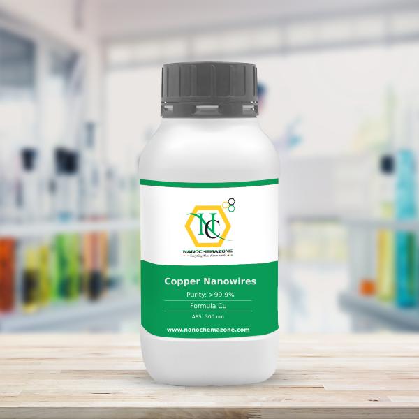
Copper Nanowires/ Cu Nanowires

$141.00
Select options This product has multiple variants. The options may be chosen on the product page
$141/5g

Product 

Copper Nanowires/ Cu Nanowires

CAS No.

7440-50-8

Appearance

Powder

Purity

≥99%,  ≥99.9%,  ≥95%

(Other purities are also available)

APS

150 nm (Size Can be customized), Ask for other available size ranges.

Ingredient

AlN

Molecular Weight

63.55 g/mol

Melting Point

1084.62 °C

Boiling Point

2562 °C

Density

8.96 g/cm³

Product Codes

NCZ-1039K

Molybdenum (Mo) Sputtering Targets, Purity: 99.95%, Size: 1”, Thickness: 0.125”

$141.00

Product 

Molybdenum (Mo) Sputtering Targets, Purity: 99.95%, Size: 1'', Thickness: 0.125''

CAS No.

 7439-98-7

Appearance

Powder

Purity

≥99%,  ≥99.9%,  ≥95%

(Other purities are also available)

APS

 N/A (Size Can be customized), Ask for other available size ranges.

Ingredient

N/A

Molecular Weight

95.95 g/mol

Melting Point

 2623 °C

Boiling Point

 4639 °C

Density

10.28 g/cm³

Product Codes

NCZ-1941K

Aluminum Silicon (AlSi) Sputtering Targets, Purity: 99.999%, Size: 1”, Thickness: 0.125”

$141.00

Product 

Aluminum Silicon (AlSi) Sputtering Targets, Purity: 99.999%, Size: 1'', Thickness: 0.125''

CAS No.

Aluminum: 7429-90-5 Silicon: 7440-21-3

Appearance

Powder

Purity

≥99%,  ≥99.9%,  ≥95%

(Other purities are also available)

APS

N/A (Size Can be customized), Ask for other available size ranges.

Ingredient

N/A

Molecular Weight

 Al: 26.98 g/mol Si: 28.09 g/mol

Melting Point

 ~577–660 °C (depends on Si content)

Boiling Point

~2519 °C (approx.)

Density

~2.6–2.7 g/cm³

Product Codes

NCZ-2519K

Graphene Oxide Water Dispersion, Purity: 99.5%, Black Liquid, GO: 2,0 wt%

Price range: $142.00 through $855.00
Select options This product has multiple variants. The options may be chosen on the product page

Graphene Oxide Water Dispersion

Purity: 99.5%, Black Liquid, GO: 2,0 wt%

Graphene Oxide Water Dispersion is black, odorless and very stable liquid which is suitable for the preparation of reduced graphene and graphene film. Graphene Oxide (GO) water dispersion has a wide range of applications such as transparent conductive films/coatings, solar energy, bio-sensing material, super capacitors and many more. Nanografi supplies graphene oxide water dispersion with high quantity and more types for different applications.

Gallium Arsenide (GaAs) Wafers, Size: 2”, Thickness: 400±25 μm, Double Side Polished, EPI-ready

Price range: $142.00 through $2,192.00
Select options This product has multiple variants. The options may be chosen on the product page
1 piece/128€ 5 pieces/490€ 25 pieces/1975€ Please contact us for quotes on larger quantities ! Gallium Arsenide (GaAs) Wafer Size: 2”, Double Side Polished, Thickness: 400± 25 μm, EPI-ready  Technical Properties:
Quality  GaAs
Materials  GaAs
Size (inch)  2”
Thickness (μm)  400± 25
Polished  Double Side
Dopant  Undoped
Orientation  100
Resistivity   1 E8
Mobility  2000
EPD  ≤5000
Growth method  VGF
OF Length  17±1
IF Length  7±1
Applications: Gallium arsenide (GaAs) is a compound of the elements gallium and arsenic. Vertical gradient freeze is the most common method to produce GaAs wafers. Mainly used for circuits, electronics and solar cell applications. Carbon, silicon, tellurium and zinc are some of the dopants that are used to modify the characteristics and electrical properties of gallium arsenide wafers. Wafer flatness and surface purity are ensured by highest quality standards. Boron concentration of gallium arsenide wafers highly depend on the production method. Gallium arsenide wafers with adequate electrical resistancy prevent high current induction in the circuit. Mobility of GaAs wafers can be tailored with different doping levels. Gallium arsenide (GaAs) is a semiconductor compound. Gallium arsenide (GaAs)  has a high electron velocity and high saturated electron mobility. This makes gallium arsenide (GaAs) components are useful in fast electronic switching applications and at ultra-high radio frequencies. In 1907, the British discovered infrared emmission from gallium arsenide. This was called electroluminescence. Also, gallium arsenide (GaAs) was used as a solar cells in space for the Venera 3 mission in 1965, which is the first known operational use of gallium arsenide (GaAs).
  • Gallium arsenide (GaAs) is used in laser diodes.
  • Gallium arsenide (GaAs) is used in solar cells.
  • Gallium arsenide (GaAs) is used in optical windows.
  • Gallium arsenide (GaAs) is used in monolithic microwave integrated circuits.
  • Gallium arsenide (GaAs) is used in microwave frequency integrated circuits.
  • Gallium arsenide (GaAs) is used in infrared light-emitting diodes.
  • Gallium arsenide (GaAs) is useful in barometers.
  • Gallium arsenide (GaAs) is useful in pharmaceuticals and nuclear medicine tests.
  • Gallium arsenide (GaAs) is useful in high temperature thermometers.

Nickel (Ni) Sputtering Targets, Purity: 99.9%, Size: 3”, Thickness: 0.125”

$142.00

Product 

Nickel (Ni) Sputtering Targets, Purity: 99.9%, Size: 3'', Thickness: 0.125''

CAS No.

7440-02-0

Appearance

Powder

Purity

≥99%,  ≥99.9%,  ≥95%

(Other purities are also available)

APS

 N/A (Size Can be customized), Ask for other available size ranges.

Ingredient

N/A

Molecular Weight

 58.69 g/mol

Melting Point

~1,453 °C

Boiling Point

~2,913 °C

Density

 8.90 g/cm³

Product Codes

NCZ-1886K