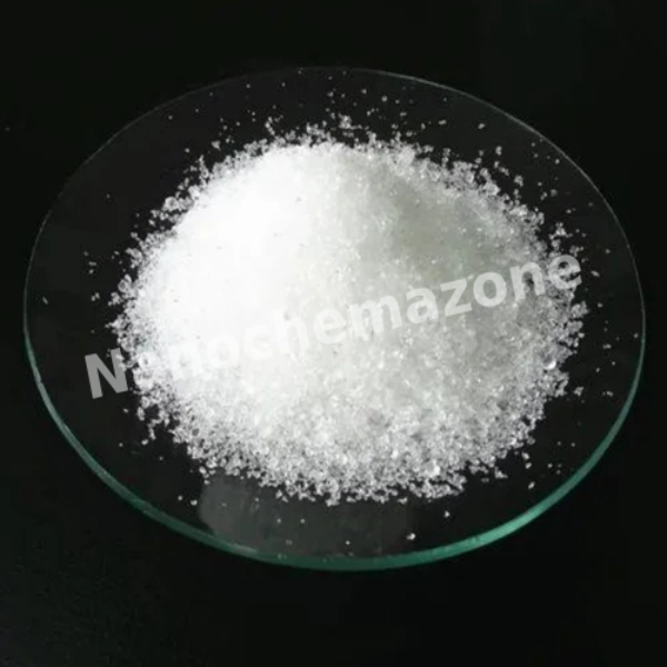
Sodium Hypophosphite Monohydrate, 99%

$95.00
Select options This product has multiple variants. The options may be chosen on the product page
Product Sodium Hypophosphite Monohydrate, 99%
CAS No. 10039-56-2
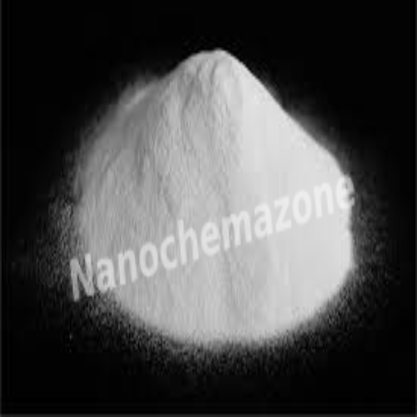
Appearance White crystalline
Purity ≥99%,  ≥99.9%,  ≥95%(Other purities are also available)
APS 1–10µm (Size Can be customized),  Ask for other available size range.
Ingredient NaH₂PO₂·H₂O
Molecular Weight 137.99 g/mol
Melting Point 150 °C
Boiling Point N/A
Density 1.96 g/cm³
Product Codes NCZ-529I

Thulium Nitrate Pentahydrate (Tm(NO3)3 · 5H2O) 99.95% 3N5

Price range: $95.00 through $315.00
Select options This product has multiple variants. The options may be chosen on the product page
Product Thulium Nitrate Pentahydrate (Tm(NO3)3 · 5H2O) 99.95% 3N5
CAS No. 10101-98-1
Appearance Colorless to pale pink crystalline
Purity ≥99%,  ≥99.9%,  ≥95%(Other purities are also available)
APS 50µm (Size Can be customized),  Ask for other available size range.
Ingredient Tm(NO3)3·5H2O
Molecular Weight 406.94 g/mol
Melting Point N/A
Boiling Point N/A
Density 2.7 g/cm³
Product Codes NCZ-557I

Graphene Ethanol Dispersion, Purity: 99.5%, Graphene: 2 wt%

Price range: $96.00 through $1,335.00
Select options This product has multiple variants. The options may be chosen on the product page
Graphene Ethanol Dispersion, Purity: 99.5%,  Graphene: 2 wt%
Graphene Purity (%) 99,5
Graphene Thickness (nm) 0,6-1,2
Diameter (µm) 2,0-12,0
Appearance Black Liquid
Concentration (wt%) 2 (mg/ml)
Specific Surface Area (m2/g) 600-1200
Elemental Analysis (%) C            O 99,6    <0,4
Surfactant                                                                                                           YES

Tin Oxide (SnO2) Nanopowder/Nanoparticles, High Purity: 99.9999%, Size: 18 nm

Price range: $96.00 through $535.00
Select options This product has multiple variants. The options may be chosen on the product page
5 grams/85 € 25 grams/173 € 100 grams/473 €
Please contact us for quotes on larger quantities !!!

Tin Oxide (SnO2) Nanopowder/Nanoparticles

High Purity: 99.9999%, Size: 18 nm

Technical Properties:

Purity (%) 99.9999
Morphology spherical
Average Particle Size (nm) 18.0
Specific Surface Area (m2/g) 45-85
Bulk Density (g/cm3) <0.5
True Density (g/cm3) 7,1
Elemental Analysis (%) Al Fe Cu Pb In
0.0002 0.001 0.002 0.0032 0.0008

Applications:

Tin oxide nanoparticles have application in electronic devices. It is used in liquid crystal displays, optoelectronic devices, solar cells, gas sensors, and resistors. It is also used in anti-static coatings, and energy conserving coatings. It has applications in catalysis. It is used in transparent heating elements

Aluminum 7075 Alloy Powder, Purity: 99.5+%, Size: <325 mesh

Price range: $96.00 through $277.00
Select options This product has multiple variants. The options may be chosen on the product page
100 grams/85 €                      
500 grams/156 €                    
1000 grams/245 € Please contact us for quotes on larger quantities !!!

Aluminum 7075 Alloy Powder

Scandium (Sc) Micron Powder Purity: 99.9 %, Particle Size: 200 mesh

Price range: $96.00 through $2,660.00
Select options This product has multiple variants. The options may be chosen on the product page
1 gram/86 € 5 grams/290 € 25 grams/864 € 100 grams/2360 €      

Niobium (Nb) Micron Powder Purity: 99.95 %, Size: 3 µm

Price range: $96.00 through $755.00
Select options This product has multiple variants. The options may be chosen on the product page
25 grams/86 € 100 grams/150 € 500 grams/573 € 1000 grams/870 €  

Aluminum (Al) Sputtering Targets, Purity: 99.99%, Size: 2”, Thickness: 0.125”

$96.00

Applications of Sputtering Targets;

  • Sputtering targets is used for film deposition. The deposition made by sputter targets is a method of depositing thin films by sputtering that involves eroding material from a "target" source onto a "substrate" such as  a silicon wafer.
  • Semiconductor sputtering targets is used to etch the target. Sputter etching is chosen in cases where a high degree of etching anisotropy is needed and selectivity is not a concern.
  • Sputter targets is also used for analysis by etching away the target material.
One of the example occurs in secondary ion spectroscopy (SIMS), where the target sample is sputtered at a constant rate. As the target is sputtered, the concentration and identity of sputtered atoms are measured using mass spectrometry. By helping of the sputtering target, the composition of the target material can be determined and even extremely low concentrations of impurities are detected. Sputtering target has also application area in space. Sputtering is one of the forms of space weathering, a process that changes the physical and chemical properties of airless bodies, such as asteroids and the Moon. Aluminum which has the chemical symbol of Al, is a silvery white, soft, ductile metal that is the third most abundant element. Aluminum is notable due to for its light weight, strength, durability and for its ability to resist corrosion. Aluminum forms an extremely thin but very strong layer of oxide film. Aluminum has also high thermal and electrical conductivity. Aluminum sputtering targets have a particularly fine-grained microstructure. This property of Aluminum sputtering targets ensures that you benefit from uniform erosion and a low susceptibility to particle formation throughout the sputtering process.

Zinc (Zn) Sputtering Targets, Purity: 99.99%, Size: 1”, Thickness: 0.250”

$96.00

Product 

Zinc (Zn) Sputtering Targets, Purity: 99.99%, Size: 1'', Thickness: 0.250''

CAS No.

7440‑66‑6

Appearance

Powder

Purity

≥99%,  ≥99.9%,  ≥95%

(Other purities are also available)

APS

Zn (black granules) (Size Can be customized), Ask for other available size ranges.

Ingredient

N/A

Molecular Weight

65.38 g/mol

Melting Point

419.5 °C

Boiling Point

 907 °C

Density

7.14 g/cm³

Product Codes

NCZ-1477K

Nickel Chromium (Ni-Cr) Alloy Nanopowder/Nanoparticles, Purity: 99.95%, Size: < 90 nm

Price range: $97.00 through $3,309.00
Select options This product has multiple variants. The options may be chosen on the product page

Nickel Chromium (Ni-Cr) Alloy Nanopowder/Nanoparticles

Purity: 99.95%, Size: < 90 nm

Technical Properties:

Alloy Ratio (Ni-Cr) 80-20
Average Particle Size (nm) < 90 nm

Properties, Storage and Cautions:

Ni-Cr alloy nanoparticles are highly reactive, therefore it should be handled with care and rapid moves, vibrations should be avoided. The powder should be kept away from sunlight, any kind of heating, moisture and impacts. Coagulation of the particles is a serious problem, so, the powder should be sealed under vacuum and should be kept in cool and dry conditions. Air contact should be avoided.

Nickel Chromium (Ni-Cr) Alloy Nanopowder/Nanoparticles, Purity: 99.95%, Size: < 90 nm

Price range: $97.00 through $3,309.00
Select options This product has multiple variants. The options may be chosen on the product page

Nickel Chromium (Ni-Cr) Alloy Nanopowder/Nanoparticles

Purity: 99.95%, Size: < 90 nm

Technical Properties:

Alloy Ratio (Ni-Cr) 80-20
Average Particle Size (nm) < 90 nm

Properties, Storage and Cautions:

Ni-Cr alloy nanoparticles are highly reactive, therefore it should be handled with care and rapid moves, vibrations should be avoided. The powder should be kept away from sunlight, any kind of heating, moisture and impacts. Coagulation of the particles is a serious problem, so, the powder should be sealed under vacuum and should be kept in cool and dry conditions. Air contact should be avoided.

Applications:

Ni-Cr alloy is generally used in electrical heaters, explosives, ignition systems, internal support for clay sculptures etc…

Nickel Chromium (Ni-Cr) Alloy Nanopowder/Nanoparticles, Purity: 99.95%, Size: < 90 nm

Price range: $97.00 through $3,309.00
Select options This product has multiple variants. The options may be chosen on the product page

Nickel Chromium (Ni-Cr) Alloy Nanopowder/Nanoparticles

Purity: 99.95%, Size: < 90 nm

Technical Properties:

Alloy Ratio (Ni-Cr) 80-20
Average Particle Size (nm) < 90 nm

Properties, Storage and Cautions:

Ni-Cr alloy nanoparticles are highly reactive, therefore it should be handled with care and rapid moves, vibrations should be avoided. The powder should be kept away from sunlight, any kind of heating, moisture and impacts. Coagulation of the particles is a serious problem, so, the powder should be sealed under vacuum and should be kept in cool and dry conditions. Air contact should be avoided.

Nickel Chromium (Ni-Cr) Alloy Nanopowder/Nanoparticles, Purity: 99.95%, Size: < 90 nm

Price range: $97.00 through $3,318.00
Select options This product has multiple variants. The options may be chosen on the product page
1 gram/86 € 5 grams/325 € 25 grams/980 € 100 grams/2924 €                     
Please contact us for quotes on larger quantities !!!

Nickel Chromium (Ni-Cr) Alloy Nanopowder/Nanoparticles

Purity: 99.95%, Size: < 90 nm

Technical Properties:

Alloy Ratio (Ni-Cr) 80-20
Average Particle Size (nm) < 90 nm

Properties, Storage and Cautions:

Ni-Cr alloy nanoparticles are highly reactive, therefore it should be handled with care and rapid moves, vibrations should be avoided. The powder should be kept away from sunlight, any kind of heating, moisture and impacts. Coagulation of the particles is a serious problem, so, the powder should be sealed under vacuum and should be kept in cool and dry conditions. Air contact should be avoided.

Applications:

Ni-Cr alloy is generally used in electrical heaters, explosives, ignition systems, internal support for clay sculptures etc…

Graphitized Carbon Nanofiber, Purity: 99.95%, Size: 200-600 nm

Price range: $97.00 through $448.00
Select options This product has multiple variants. The options may be chosen on the product page

Applications:

The chemical vapor deposition (CVD) process yields extremely pure carbon nanofibers (>99,9%). Following a 24-hour annealing process at approximately 3000 degrees Celsius (graphitization), this high level of purity, electrical and characteristics of thermal conductivity. Because of its conductivity, carbon nanofiber (CNF), a material similar to carbon nanotubes, is appealing as well as mechanical qualities. It is widely employed and researched in energy conversion, chemical catalysis, sensors, electrodes, lithography, EMI shielding, super capacitors, hydrogen storage, rechargeable batteries, and displays, biomedical research, composite and polymer reinforcement projects, etc.

Prime FZ-Si Wafer, Size: 4”, Orientation: (100), Phosphor Doped, Resistivity: 5000 – 500000 (ohm.cm), 2-Side Polished, Thickness: 300 ± 10 μm

Price range: $97.00 through $1,638.00
Select options This product has multiple variants. The options may be chosen on the product page
Prime FZ-Si Wafer Size: 4”, Orientation: (100), Phosphor Doped, 2-Side Polished, Thickness: 300 ± 10 μm Technical Properties: Quality Prime

Prime FZ-Si Wafer, Size: 4”, Orientation: (100), Phosphor Doped, Resistivity: 3000 – 100000 (ohm.cm), 2-Side Polished, Thickness: 200 ± 10 μm

Price range: $97.00 through $1,638.00
Select options This product has multiple variants. The options may be chosen on the product page
Prime FZ-Si Wafer Size: 4”, Orientation: (100), Phosphor Doped, 2-Side Polished, Thickness: 200 ± 10 μm Technical Properties: Quality Prime

Aluminum (Al) Sputtering Targets, Purity: 99.99%, Size: 1”, Thickness: 0.250”

$97.00

 Applications of Sputtering Targets;

  • Sputtering targets is used for film deposition. The deposition made by sputter targets is a method of depositing thin films by sputtering that involves eroding material from a "target" source onto a "substrate" such as  a silicon wafer.
  • Semiconductor sputtering targets is used to etch the target. Sputter etching is chosen in cases where a high degree of etching anisotropy is needed and selectivity is not a concern.
  • Sputter targets is also used for analysis by etching away the target material.
One of the example occurs in secondary ion spectroscopy (SIMS), where the target sample is sputtered at a constant rate. As the target is sputtered, the concentration and identity of sputtered atoms are measured using mass spectrometry. By helping of the sputtering target, the composition of the target material can be determined and even extremely low concentrations of impurities are detected. Sputtering target has also application area in space. Sputtering is one of the forms of space weathering, a process that changes the physical and chemical properties of airless bodies, such as asteroids and the Moon. Aluminum which has the chemical symbol of Al, is a silvery white, soft, ductile metal that is the third most abundant element. Aluminum is notable due to for its light weight, strength, durability and for its ability to resist corrosion. Aluminum forms an extremely thin but very strong layer of oxide film. Aluminum has also high thermal and electrical conductivity. Aluminum sputtering targets have a particularly fine-grained microstructure. This property of Aluminum sputtering targets ensures that you benefit from uniform erosion and a low susceptibility to particle formation throughout the sputtering process.

Tin (Sn) Sputtering Targets, Purity: 99.99%, Size: 1”, Thickness: 0.125”

$97.00

Applications of Sputtering Targets;

Film deposition is accomplished using sputtering targets. A technique for sputtering thin films is called "deposition made by sputter targets," which entails eroding material from a "target" source onto a "substrate" like a silicon wafer. Etching of the target is done using semiconductor sputtering targets. When selectivity is not an issue and a high degree of etching anisotropy is required, sputter etching is the method of choice. By removing the target material through etching, sputter targets are also utilized for investigation. In secondary ion spectroscopy (SIMS), one example is when the target material is sputtered at a steady pace. Mass spectrometry is used to quantify the concentration and identity of spewed atoms as the target is sputtered.

The target material's composition may be ascertained and even very low concentrations of contaminants can be found with the aid of the sputtering target.

There is also an application area for sputtering targets in space. One type of space weathering that alters the chemical and physical characteristics of airless worlds like the Moon and asteroids is sputtering.

Tin (Sn) Sputtering Targets, Purity: 99.99%, Size: 1”, Thickness: 0.125”

$97.00

Applications of Sputtering Targets;

Film deposition is accomplished using sputtering targets. A technique for sputtering thin films is called "deposition made by sputter targets," which entails eroding material from a "target" source onto a "substrate" like a silicon wafer. Etching of the target is done using semiconductor sputtering targets. When selectivity is not an issue and a high degree of etching anisotropy is required, sputter etching is the method of choice. By removing the target material through etching, sputter targets are also utilized for investigation. In secondary ion spectroscopy (SIMS), one example is when the target material is sputtered at a steady pace. Mass spectrometry is used to quantify the concentration and identity of spewed atoms as the target is sputtered.

The target material's composition may be ascertained and even very low concentrations of contaminants can be found with the aid of the sputtering target.

There is also an application area for sputtering targets in space. One type of space weathering that alters the chemical and physical characteristics of airless worlds like the Moon and asteroids is sputtering.

Cerium Oxide Nanopowder/ Nanoparticles (CeO2, 100~1000nm)

Price range: $97.00 through $271.00
Select options This product has multiple variants. The options may be chosen on the product page
$97/100g
$185/500g
$271/kg

Product 

Cerium Oxide Nanopowder/ Nanoparticles (CeO2, 100~1000nm)

CAS No.

1306-38-3

Appearance

Powder

Purity

≥99%,  ≥99.9%,  ≥95%

(Other purities are also available)

APS

100~1000nm (Size Can be customized), Ask for other available size ranges.

Ingredient

N/A

Molecular Weight

172.11 g/mol

Melting Point

 ~2,400 °C

Boiling Point

~3,500 °C

Density

~7.13 g/cm³

Product Codes

NCZ-1118K

Cerium Oxide Nanopowder/ Nanoparticles (CeO2, 100~1000nm, 99.9%)

Price range: $97.00 through $185.00
Select options This product has multiple variants. The options may be chosen on the product page
$97/100g $185/500g $271/kg
Product Cerium Oxide Nanopowder/ Nanoparticles (CeO2, 100~1000nm, 99.9%)
CAS No. 1306-38-3
Appearance Pale yellow to white powder
Purity ≥99%,  ≥99.9%,  ≥95%(Other purities are also available)
APS 100 - 1000 nm (Size Can be customized),  Ask for other available size range.
Ingredient CeO2
Molecular Weight 172.11g/mol
Melting Point 2400°C
Boiling Point 3500°C
Density N/A
Product Codes NCZ-101R
 

High Purity Short MWNTs 95+%, 8~15nm

Price range: $97.00 through $673.00
Select options This product has multiple variants. The options may be chosen on the product page
$97/5g
$297/25g
$673/100g

Product 

High Purity Short MWNTs 95+%, 8~15nm

CAS No.

 7727-54-0

Appearance

Powder

Purity

≥99%,  ≥99.9%,  ≥95%

(Other purities are also available)

APS

8~15nm (Size Can be customized), Ask for other available size ranges.

Ingredient

N/A

Molecular Weight

228.20 g/mol

Melting Point

 120 °C

Boiling Point

N/A

Density

 1.98 g/cm³

Product Codes

NCZ-1242K

4N (99.99%) Silicon Dioxide (SiO2) Pieces Evaporation Materials

Price range: $97.00 through $183.00
Select options This product has multiple variants. The options may be chosen on the product page
Product 4N (99.99%) Silicon Dioxide (SiO2) Pieces Evaporation Materials
CAS No. 14808-60-7
Appearance White, Crystalline Solid 
Purity ≥99%,  ≥99.9%,  ≥95%(Other purities are also available)
APS 1–10mm (Size Can be customized),  Ask for other available size range.
Ingredient SiO2
Molecular Weight 60.084 g/mol
Melting Point 1,713°C
Boiling Point 2,230°C
Density 2.196 g/cm³
Product Codes NCZ-109E
 

4N (99.99%) Tungsten Oxide (WO3) Pieces (3-12mm) Evaporation Materials

Price range: $97.00 through $865.00
Select options This product has multiple variants. The options may be chosen on the product page
Product 4N (99.99%) Tungsten Oxide (WO3) Pieces (3-12mm) Evaporation Materials
CAS No. 1314-35-8
Appearance Lemon Yellow, Solid 
Purity ≥99%,  ≥99.9%,  ≥95%(Other purities are also available)
APS 3-12mm (Size Can be customized),  Ask for other available size range.
Ingredient WO3
Molecular Weight 231.85 g/mol
Melting Point 1,473 °C
Boiling Point N/A
Density 7.16 g/cm³
Product Codes NCZ-138E
 

4N (99.99%) Silicon Monoxide (SiO) Pieces (1-3mm) Evaporation Materials

Price range: $97.00 through $594.00
Select options This product has multiple variants. The options may be chosen on the product page
Product 4N (99.99%) Silicon Monoxide (SiO) Pieces (1-3mm) Evaporation Materials
CAS No. 10097-28-6
Appearance Brown/Black Glassy
Purity ≥99%,  ≥99.9%,  ≥95%(Other purities are also available)
APS 1-3mm (Size Can be customized),  Ask for other available size range.
Ingredient SiO
Molecular Weight 44.08 g/mol
Melting Point N/A
Boiling Point N/A
Density 2.13 g/cm3
Product Codes NCZ-156E
 

3N5 (99.95%) Manganese (Mn) Pieces (3-12mm) Evaporation Materials

Price range: $97.00 through $528.00
Select options This product has multiple variants. The options may be chosen on the product page
Product 3N5 (99.95%) Manganese (Mn) Pieces (3-12mm) Evaporation Materials
CAS No. 7439-96-5
Appearance Silvery Metallic
Purity ≥99%,  ≥99.9%,  ≥95%(Other purities are also available)
APS 3-12mm (Size Can be customized),  Ask for other available size range.
Ingredient Mn
Molecular Weight 54.94 g/mol
Melting Point 1,244 °C
Boiling Point N/A
Density 77.2 g/cm3
Product Codes NCZ-159E

4N (99.99%) Silicon Monoxide (SiO) Pieces (1-3mm) Evaporation Materials

Price range: $97.00 through $594.00
Select options This product has multiple variants. The options may be chosen on the product page
Product 4N (99.99%) Silicon Monoxide (SiO) Pieces (1-3mm) Evaporation Materials
CAS No. 10097-28-6
Appearance Black to brownish
Purity ≥99%,  ≥99.9%,  ≥95%(Other purities are also available)
APS 1-3mm (Size Can be customized),  Ask for other available size range.
Ingredient SiO
Molecular Weight 44.08 g/mol
Melting Point 1,910 °C
Boiling Point N/A
Density 2.13 g/cm³
Product Codes NCZ-171I

4N (99.99%) Tungsten Oxide (WO3) Pieces (3-12mm) Evaporation Materials

Price range: $97.00 through $865.00
Select options This product has multiple variants. The options may be chosen on the product page
Product 4N (99.99%) Tungsten Oxide (WO3) Pieces (3-12mm) Evaporation Materials
CAS No. 1314-35-8
Appearance Lemon Yellow, Solid
Purity ≥99%,  ≥99.9%,  ≥95%(Other purities are also available)
APS 3-12mm (Size Can be customized),  Ask for other available size range.
Ingredient WO3
Molecular Weight 231.85 g/mol
Melting Point N/A
Boiling Point N/A
Density 7.16 g/cm³
Product Codes NCZ-175I

Iron (Fe) Sputtering Targets, Purity: 99.95%, Size: 1”, Thickness: 0.250”

$97.00

Product 

Iron (Fe) Sputtering Targets, Purity: 99.95%, Size: 1'', Thickness: 0.250''

CAS No.

 7439-89-6

Appearance

Powder

Purity

≥99%,  ≥99.9%,  ≥95%

(Other purities are also available)

APS

 N/A (Size Can be customized), Ask for other available size ranges.

Ingredient

N/A

Molecular Weight

 55.85 g/mol

Melting Point

 1538 °C

Boiling Point

 2862 °C

Density

 7.87 g/cm³

Product Codes

NCZ-2190K

Yttrium (III) Oxide (Y2O3) 99.999% 5N Powder (5-8 um)

Price range: $97.00 through $425.00
Select options This product has multiple variants. The options may be chosen on the product page
Product Yttrium (III) Oxide (Y2O3) 99.999% 5N Powder (5-8 um)
CAS No. 1314-36-9
Appearance White
Purity ≥99%,  ≥99.9%,  ≥95%(Other purities are also available)
APS 5-8um (Size Can be customized),  Ask for other available size range.
Ingredient Y₂O₃
Molecular Weight 225.81 g/mol
Melting Point N/A
Boiling Point N/A
Density 5.01 g/cm³
Product Codes NCZ-602I

PPL Inside Chamber for Hydrothermal Synthesis Autoclave Reactors

Price range: $97.50 through $293.75
Select options This product has multiple variants. The options may be chosen on the product page
50ml   97,5€ 100ml  106,25€ 500ml  293,75€ Product Information Product Name PPL Inside Chamber for Hydrothermal Synthesis Autoclave Reactors Size

Fullerene-C60, Purity: 99.9%

Price range: $98.00 through $442.00
Select options This product has multiple variants. The options may be chosen on the product page
1 gram/88 € 5 grams/395 €                           
Please contact us for quotes on larger quantities !!!

Fullerene-C60

Purity: 99.9% 

Technical Properties:

Fullerene Compound Formula C60
Fullerene  Molecular Weight 720.64
Fullerene  Size Diameter: 0.8 nm, Length: 1.2 nm
Fullerene  Purity 99.9%
Fullerene  Melting Point >280 °C
Fullerene  True Density 1.71 g/cm3
Fullerene  Electrical Resistivity 1034 ohms m-1
Fullerene  Appearance Shinning Black
Fullerene  CAS 99685-96-8 

Applications:

1. Pharmaceutical: Diagnostic reagents, super drugs, cosmetics, nuclear magnetic resonance (NMR) with the developer. DNA affinity 2. Energy: Solar battery, fuel cell, secondary battery. 3. Industry: Wear resistant material, flame retardant materials, lubricants, polymer additives, high-performance membrane, catalyst, artificial diamond, hard alloy, electric viscous fluid, ink filters, high-performance coatings, fire retardant coatings, manufacturing bioactive materials , memory materials, embedded molecular and other characteristics, composite materials etc. 4. Information industry: Semiconductor record medium, magnetic materials, printing ink, toner, ink, paper special purposes. 5. Electronic parts: Superconducting semiconductor, diodes, transistors, inductor.  , 6. Optical materials, electronic camera, fluorescence display tube, nonlinear optical materials. 7. Environment: Gas adsorption, gas storage.  

Carbon Nanotubes Doped with 52 wt% Iron Oxide (Fe3O4) Nanopowder/Nanoparticles

Price range: $98.00 through $544.00
Select options This product has multiple variants. The options may be chosen on the product page

Carbon nanotubes doped with metal oxide nanopowders improve electrical and mechanical properties significantly. Hardness, tensile strength, specific strength, and elastic modulus are examples of such enhancements. As a result of these advancements, these materials are now widely used for a variety of purposes.

applications. Among these applications are drug delivery, biosensors, 3-CNT composites, 4-catalysis, 5-nanoprobes, and 6-hydrogen storage. 8 gas-discharge tubes, 7 lithium batteries nine flat panel displays 10-supercapacitors, 11-transistors, twelve solar cells, 13-photoluminescence, 14-templates  

Graphene Sheet, Size: 29 cm x 39 cm, Thickness: 35 µm, Highly Conductive

Price range: $98.00 through $1,150.00
Select options This product has multiple variants. The options may be chosen on the product page

Applications:

  • Consumer electronics: smartphones, tablets, PCs, TVs
  • LED lighting
  • Energy storage
  • Automotive
  • Industrial
  • Medical
  • Military and aerospace

Copper (Cu) Sputtering Targets, Purity: 99.99%, Size: 3”, Thickness: 0.250”

$98.00

Applications of Sputtering Targets;

Film deposition is accomplished using sputtering targets. A technique for sputtering thin films is called "deposition made by sputter targets," which entails eroding material from a "target" source onto a "substrate" like a silicon wafer. Etching of the target is done using semiconductor sputtering targets. When selectivity is not an issue and a high degree of etching anisotropy is required, sputter etching is the method of choice. By removing the target material through etching, sputter targets are also utilized for investigation. In secondary ion spectroscopy (SIMS), one example is when the target material is sputtered at a steady pace. Mass spectrometry is used to quantify the concentration and identity of spewed atoms as the target is sputtered.

The target material's composition may be ascertained and even very low concentrations of contaminants can be found with the aid of the sputtering target.

There is also an application area for sputtering targets in space. One type of space weathering that alters the chemical and physical characteristics of airless worlds like the Moon and asteroids is sputtering.

Iron (Fe) Sputtering Targets, Purity: 99.9%, Size: 3”, Thickness: 0.125”

$98.00

Applications of Sputtering Targets;

Film deposition is accomplished using sputtering targets. A technique for sputtering thin films is called "deposition made by sputter targets," which entails eroding material from a "target" source onto a "substrate" like a silicon wafer. Etching of the target is done using semiconductor sputtering targets. When selectivity is not an issue and a high degree of etching anisotropy is required, sputter etching is the method of choice. By removing the target material through etching, sputter targets are also utilized for investigation. In secondary ion spectroscopy (SIMS), one example is when the target material is sputtered at a steady pace. Mass spectrometry is used to quantify the concentration and identity of spewed atoms as the target is sputtered.

The target material's composition may be ascertained and even very low concentrations of contaminants can be found with the aid of the sputtering target.

There is also an application area for sputtering targets in space. One type of space weathering that alters the chemical and physical characteristics of airless worlds like the Moon and asteroids is sputtering.

Zinc (Zn) Sputtering Targets, Purity: 99.99%, Size: 2”, Thickness: 0.125”

$98.00

Applications of Sputtering Targets;

Film deposition is accomplished using sputtering targets. A technique for sputtering thin films is called "deposition made by sputter targets," which entails eroding material from a "target" source onto a "substrate" like a silicon wafer. Etching of the target is done using semiconductor sputtering targets. When selectivity is not an issue and a high degree of etching anisotropy is required, sputter etching is the method of choice. By removing the target material through etching, sputter targets are also utilized for investigation. In secondary ion spectroscopy (SIMS), one example is when the target material is sputtered at a steady pace. Mass spectrometry is used to quantify the concentration and identity of spewed atoms as the target is sputtered.

The target material's composition may be ascertained and even very low concentrations of contaminants can be found with the aid of the sputtering target.

There is also an application area for sputtering targets in space. One type of space weathering that alters the chemical and physical characteristics of airless worlds like the Moon and asteroids is sputtering.

Molybdenum (Mo) Sputtering Target

Price range: $98.00 through $414.00
Select options This product has multiple variants. The options may be chosen on the product page

Product 

Molybdenum (Mo) Sputtering Target

CAS No.

7439-96-5

Appearance

Powder

Purity

≥99%,  ≥99.9%,  ≥95%

(Other purities are also available)

APS

 NA (Size Can be customized), Ask for other available size ranges.

Ingredient

N/A

Molecular Weight

54.938 g/mol

Melting Point

1,246 °C

Boiling Point

2,061 °C

Density

1.738 g/cm³

Product Codes

NCZ-1298K

Hafnium Carbide (HfC) Nanopowder/Nanoparticles, Purity: 99.99%, Size: 790 nm, Cubic

Price range: $99.00 through $690.00
Select options This product has multiple variants. The options may be chosen on the product page
1 gram/88 € 5 grams/248 € 
25 grams/609 €                       
Please contact us for quotes on larger quantities !!! 

Hafnium Carbide (HfC) Nanopowder/Nanoparticles

Purity: 99.99%, Size: 790 nm, Cubic

Applications:

Hafnium carbide powder is very hard material. It is used in hard coatings. It is also used as rocket nozzle throat material and in metal ceramic materials.

Graphite Sheet Thermal Interface Material, EYG Series, 1600 W/m.K, Thickness: 25 µm, Lenght: 230 mm, Width: 180 mm

Price range: $99.00 through $432.00
Select options This product has multiple variants. The options may be chosen on the product page
1 piece / 99 € 5 pieces / 432 € Please contact us for quotes on larger quantities !   Graphite

Fullerene-C60, Purity: 99.5%

Price range: $99.00 through $450.00
Select options This product has multiple variants. The options may be chosen on the product page

Applications:

1. Pharmaceutical: Diagnostic reagents, super drugs, cosmetics, nuclear magnetic resonance (NMR) with the developer. DNA affinity 2. Energy: Solar battery, fuel cell, secondary battery. 3. Industry: Wear resistant material, flame retardant materials, lubricants, polymer additives, high-performance membrane, catalyst, artificial diamond, hard alloy, electric viscous fluid, ink filters, high-performance coatings, fire retardant coatings, manufacturing bioactive materials , memory materials, embedded molecular and other characteristics, composite materials etc. 4. Information industry: Semiconductor record medium, magnetic materials, printing ink, toner, ink, paper special purposes. 5. Electronic parts: Superconducting semiconductor, diodes, transistors, inductor.  , 6. Optical materials, electronic camera, fluorescence display tube, nonlinear optical materials. 7. Environment: Gas adsorption, gas storage.

Polyhydroxylated Fullerene (Fullerenols)/ C60, (-OH) Functionalized, Dispersed in Water, 80 ppm Dry powder

Price range: $99.00 through $2,050.00
Select options This product has multiple variants. The options may be chosen on the product page

Applications:

1. Pharmaceutical: Diagnostic reagents, super drugs, cosmetics, nuclear magnetic resonance (NMR) with the developer. DNA affinity, anti-HIV drugs, anti-cancer drugs, chemotherapy drugs, cosmetics additives and scientific research. 2. Energy: Solar battery, fuel cell, secondary battery. 3. Industry: Wear resistant material, flame retardant materials, lubricants, polymer additives, high-performance membrane, catalyst, artificial diamond, hard alloy, electric viscous fluid, ink filters, high-performance coatings, fire retardant coatings, manufacturing bioactive materials , memory materials, embedded molecular and other characteristics, composite materials etc. 4. Information industry: Semiconductor record medium, magnetic materials, printing ink, toner, ink, paper special purposes. 5. Electronic parts: Superconducting semiconductor, diodes, transistors, inductor.  , 6. Optical materials, electronic camera, fluorescence display tube, nonlinear optical materials. 7. Environment: Gas adsorption, gas storage.

Tungsten Titanium (TiW) Sputtering Targets, Purity: 99.99%, Size: 1”, Thickness: 0.250”

$99.00

Applications of Sputtering Targets;

Film deposition is accomplished using sputtering targets. A technique for sputtering thin films is called "deposition made by sputter targets," which entails eroding material from a "target" source onto a "substrate" like a silicon wafer. Etching of the target is done using semiconductor sputtering targets. When selectivity is not an issue and a high degree of etching anisotropy is required, sputter etching is the method of choice. By removing the target material through etching, sputter targets are also utilized for investigation. In secondary ion spectroscopy (SIMS), one example is when the target material is sputtered at a steady pace. Mass spectrometry is used to quantify the concentration and identity of spewed atoms as the target is sputtered.

The target material's composition may be ascertained and even very low concentrations of contaminants can be found with the aid of the sputtering target.

There is also an application area for sputtering targets in space. One type of space weathering that alters the chemical and physical characteristics of airless worlds like the Moon and asteroids is sputtering.

3N (99.9%) Zinc Oxide (ZnO) Pieces (1-3mm) Evaporation Materials

Price range: $99.00 through $405.00
Select options This product has multiple variants. The options may be chosen on the product page
Product 3N (99.9%) Zinc Oxide (ZnO) Pieces (1-3mm) Evaporation Materials
CAS No. 1314-13-2
Appearance White, Crystalline Solid powder
Purity ≥99%,  ≥99.9%,  ≥95%(Other purities are also available)
APS 1-3mm (Size Can be customized),  Ask for other available size range.
Ingredient ZnO
Molecular Weight 81.38 g/mol
Melting Point 1,975°C
Boiling Point N/A
Density 5.61 g/cm³
Product Codes NCZ-117E

Zirconium Sputtering Target Zr

Price range: $99.00 through $1,089.00
Select options This product has multiple variants. The options may be chosen on the product page
Product Zirconium Sputtering Target Zr
CAS No. 7440-67-7
Appearance Silvery-white, lustrous metal. 
Purity ≥99%,  ≥99.9%,  ≥95%(Other purities are also available)
APS N/A
Ingredient Zr
Molecular Weight 91.224 g/mol
Melting Point N/A
Boiling Point N/A
Density 6.52 g/cm³
Product Codes NCZ-150H

Aqueous Dispersion of PEDT/PSS Conductive Polymer (Clevios P VP CH 8000), OLED Grade (Hole-injection Material)

Price range: $99.00 through $281.00
Select options This product has multiple variants. The options may be chosen on the product page
Product Aqueous Dispersion of PEDT/PSS Conductive Polymer (Clevios P VP CH 8000), OLED Grade (Hole-injection Material)
CAS No. 155090-83-8
Appearance Dark blue to blue-black
Purity ≥99%,  ≥99.9%,  ≥95%(Other purities are also available)
APS N/A
Ingredient (C8H7SO3Na)m​
Molecular Weight N/A
Melting Point N/A
Boiling Point N/A
Density 1.0–1.1 g/cm³
Product Codes NCZ-292I

Magnesium (Mg) Sputtering Targets, Purity: 99.95%, Size: 1”, Thickness: 0.125”

$99.00

Product 

Magnesium (Mg) Sputtering Targets, Purity: 99.95%, Size: 1'', Thickness: 0.125''

CAS No.

7439-95-4

Appearance

Powder

Purity

≥99%,  ≥99.9%,  ≥95%

(Other purities are also available)

APS

 N/A (Size Can be customized), Ask for other available size ranges.

Ingredient

N/A

Molecular Weight

 24.305 g/mol

Melting Point

 650 °C

Boiling Point

 1,090 °C

Density

1.738 g/cm³

Product Codes

NCZ-2007K

Copper (Cu) Sputtering Targets, Purity: 99.999%, Size: 1”, Thickness: 0.250”

$99.00

Product 

Copper (Cu) Sputtering Targets, Purity: 99.999%, Size: 1'', Thickness: 0.250''

CAS No.

7440-50-8

Appearance

Powder

Purity

≥99%,  ≥99.9%,  ≥95%

(Other purities are also available)

APS

 N/A (Size Can be customized), Ask for other available size ranges.

Ingredient

N/A

Molecular Weight

63.55 g/mol

Melting Point

1,084 °C

Boiling Point

 2,562 °C

Density

8.96 g/cm³

Product Codes

NCZ-2271K

Quartz Wafer, (ST-Cut), Size: 4”, 1-Side Polished, Thickness: 625 ± 25 μm

Price range: $100.00 through $1,758.00
Select options This product has multiple variants. The options may be chosen on the product page
Quartz Wafer (ST-Cut), Size: 4”, 1-Side Polished, Thickness: 625 ± 25 μm Technical Properties: Quality Prime Materials Quartz Size (inch) 4”

Quartz Wafer, (AT-Cut), Size: 4”, 2-Side Polished, Thickness: 500 ± 25 μm

Price range: $100.00 through $1,758.00
Select options This product has multiple variants. The options may be chosen on the product page
Quartz Wafer (AT-Cut), Size: 4”, 2-Side Polished, Thickness: 500 ± 25 μm Technical Properties: Quality Prime Materials Quartz Size (inch)

Quartz Wafer, (X-Cut), Size: 4”, 2-Side Polished, Thickness: 300 ± 25 μm

Price range: $100.00 through $1,758.00
Select options This product has multiple variants. The options may be chosen on the product page
Quartz Wafer (X-Cut), Size: 4”, 2-Side Polished, Thickness: 300 ± 25 μm Technical Properties: Quality Prime Materials Quartz Size (inch) 4” Orientation

Carbon (C) (Graphite) Sputtering Targets, Purity: 99.999%, Size: 1”, Thickness: 0.250”

$100.00

Applications of Sputtering Targets;

Film deposition is accomplished using sputtering targets. A technique for sputtering thin films is called "deposition made by sputter targets," which entails eroding material from a "target" source onto a "substrate" like a silicon wafer. Etching of the target is done using semiconductor sputtering targets. When selectivity is not an issue and a high degree of etching anisotropy is required, sputter etching is the method of choice. By removing the target material through etching, sputter targets are also utilized for investigation. In secondary ion spectroscopy (SIMS), one example is when the target material is sputtered at a steady pace. Mass spectrometry is used to quantify the concentration and identity of spewed atoms as the target is sputtered.

The target material's composition may be ascertained and even very low concentrations of contaminants can be found with the aid of the sputtering target.

There is also an application area for sputtering targets in space. One type of space weathering that alters the chemical and physical characteristics of airless worlds like the Moon and asteroids is sputtering.

Niobium (Nb) Sputtering Targets, Purity: 99.95% pure Ex Ta, Size: 4”, Thickness: 0.250”

$100.00

Applications of Sputtering Targets;

Film deposition is accomplished using sputtering targets. A technique for sputtering thin films is called "deposition made by sputter targets," which entails eroding material from a "target" source onto a "substrate" like a silicon wafer. Etching of the target is done using semiconductor sputtering targets. When selectivity is not an issue and a high degree of etching anisotropy is required, sputter etching is the method of choice. By removing the target material through etching, sputter targets are also utilized for investigation. In secondary ion spectroscopy (SIMS), one example is when the target material is sputtered at a steady pace. Mass spectrometry is used to quantify the concentration and identity of spewed atoms as the target is sputtered.

The target material's composition may be ascertained and even very low concentrations of contaminants can be found with the aid of the sputtering target.

There is also an application area for sputtering targets in space. One type of space weathering that alters the chemical and physical characteristics of airless worlds like the Moon and asteroids is sputtering.

Nickel (Ni) Sputtering Targets, Purity: 99.9%, Size: 2”, Thickness: 0.125”

$100.00

Product 

Nickel (Ni) Sputtering Targets, Purity: 99.9%, Size: 2'', Thickness: 0.125''

CAS No.

7440-02-0

Appearance

Powder

Purity

≥99%,  ≥99.9%,  ≥95%

(Other purities are also available)

APS

 N/A (Size Can be customized), Ask for other available size ranges.

Ingredient

N/A

Molecular Weight

 58.69 g/mol

Melting Point

~1,453 °C

Boiling Point

~2,913 °C

Density

 8.90 g/cm³

Product Codes

NCZ-1892K

Aluminum Silicon Copper (AlSiCu) Sputtering Targets, Purity: 99.999%, Size: 4”, Thickness: 0.250”

$100.00

Product 

Aluminum Silicon Copper (AlSiCu) Sputtering Targets, Purity: 99.999%, Size: 4'', Thickness: 0.250''

CAS No.

Aluminum: 7429-90-5 Silicon: 7440-21-3 Copper: 7440-50-8

Appearance

Powder

Purity

≥99%,  ≥99.9%,  ≥95%

(Other purities are also available)

APS

N/A (Size Can be customized), Ask for other available size ranges.

Ingredient

N/A

Molecular Weight

Weighted average depending on composition (example below)

Melting Point

 Approx. 570–660 °C

Boiling Point

 Approx. 2500–2650 °C

Density

~2.7 to 2.9 g/cm³

Product Codes

NCZ-2520K

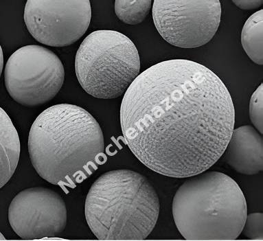
Spherical Alumina(45μm) (145559)

$100.00
Select options This product has multiple variants. The options may be chosen on the product page
Spherical Alumina(45μm) (145559)
Typical Physical Data
Items Unit Typical value Test Method
Particle Size Distribution D10 μm 22.47 Layer analyzer
D50 μm 48.9
D90 μm 90.6
Specific Surface Area m2/g 0.2 BET method
Specific Gravity g/cm3 3.7 pycnometer method
Electrical Conductivity μS/cm 24.3 Conductivity Meter
pH - 6.8 pH Meter
Circularity % 94.0 Particle Image Analyzer
 
Typical Chemical data
Test Items Unit Typical value Test Method
Chemical Analysis Al2O3 % 99.6 ICP
Na2O ppm 95.0 ICP
SiO2 ppm 83.0 ICP
Fe2O3 ppm 109.0 ICP
Ionic  Impurities Na+ ppm 45.0 Atomic Absorption Spectrometer
Cl- ppm 1.9 Auto Electric Potential Titrator
Fe++ ppm 12.3 IC
    Product Codes- NCZ-2679K

Spherical Alumina(70μm) (170559)

$100.00
Select options This product has multiple variants. The options may be chosen on the product page
Spherical Alumina(70μm) (170559)
Typical Physical Data
Items Unit Typical value Test Method
Particle Size Distribution D10 μm 47.3 Layer analyzer
D50 μm 77.7
D90 μm 125.6
Specific Surface Area m2/g 0.2 BET method
Specific Gravity g/cm3 3.8 pycnometer method
Electrical Conductivity μS/cm 17.0 Conductivity Meter
pH - 7.0 pH Meter
Circularity % 93.0 Particle Image Analyzer
 
Typical Chemical data
Test Items Unit Typical value Test Method
Chemical Analysis Al2O3 % 99.6 ICP
Na2O ppm 101.0 ICP
SiO2 ppm 82.0 ICP
Fe2O3 ppm 103.0 ICP
Ionic  Impurities Na+ ppm 45.7 Atomic Absorption Spectrometer
Cl- ppm 1.2 Auto Electric Potential Titrator
Fe++ ppm 19.2 IC
  Product Codes- NCZ-2680K

Single Walled Carbon Nanotubes, Purity: > 92%, OD: 1-2 nm

Price range: $101.00 through $4,957.00
Select options This product has multiple variants. The options may be chosen on the product page

Applications:

Single Walled Carbon Nanotubes have a variety of potential applications in different fields. These applications include medicine, mechanics, electric-electronics, chemicals, energy and others. It can be applied in, 1-drug delivery, 2-biosensors, 3-CNT composites, 4-catalysis, 5-nanoprobes, 6-hydrogen storage, 7-lithium batteries, 8-gas-discharge tubes, 9-flat panel displays, 10-supercapacitors, 11-transistors, 12-solar cells, 13-photoluminescence, 14-templates

(-COOH) Functionalized Short Single Walled Carbon Nanotubes, Purity: > 65%

Price range: $101.00 through $1,086.00
Select options This product has multiple variants. The options may be chosen on the product page

Applications:

Single Walled Carbon Nanotubes have a variety of potential applications in different fields. These applications include medicine, mechanics, electric-electronics, chemicals, energy and others. It can be applied in, 1-drug delivery, 2-biosensors, 3-CNT composites, 4-catalysis, 5-nanoprobes, 6-hydrogen storage, 7-lithium batteries, 8-gas-discharge tubes, 9-flat panel displays, 10-supercapacitors, 11-transistors, 12-solar cells, 13-photoluminescence, 14-templates  

Scandium (Sc) Micron Powder Purity: 99.5 %, Size: 325 mesh

Price range: $101.00 through $2,794.00
Select options This product has multiple variants. The options may be chosen on the product page
1 gram/90 € 5 grams/294 € 25 grams/885 € 100 grams/2479 €