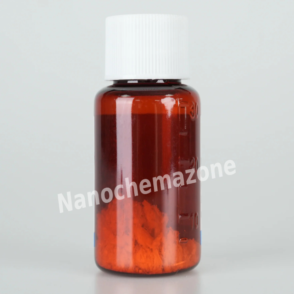
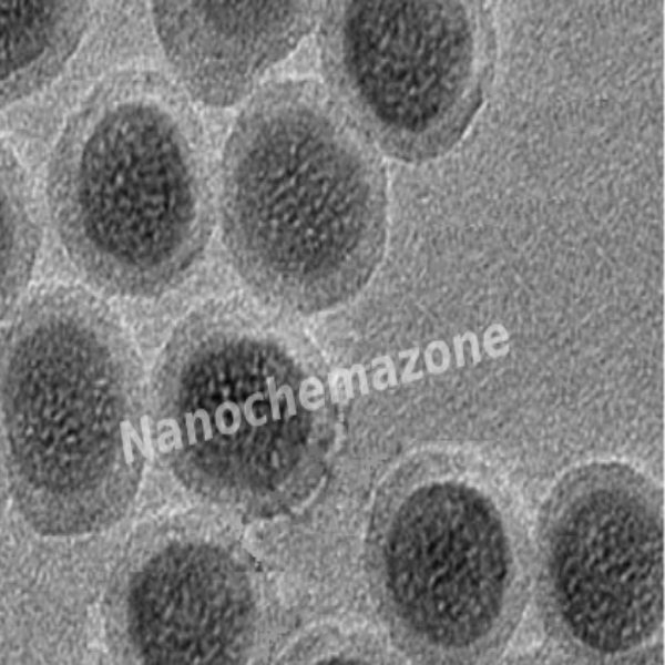
Copper (Cu) Nanopowder/Nanoparticles
Purity: 99.85%, Size: 22 nm, Partially Passivated
Technical Properties:
| Cu Purity (%) |
≥99,8 |
(partially passivated by coating nanoparticles with 0,8 wt% Oxygen for only safe shipping) |
| Bulk Density (g/cm3) |
0,2-0,4 |
|
|
| True Density (g/cm3) |
8,9 |
|
|
| Color |
dark brown |
|
|
| Shape |
spherical |
|
|
| Crystal Structure |
cubic |
|
|
| Average Particle Size (nm) |
22 |
|
|
| Specific Surface Area (m2/g) |
35,0-55,0 |
|
|
| Elemental Analysis |
Cu |
Si |
Others |
|
≥99.8 |
0.1 |
≤0.01 |
Properties, Storage and Cautions:
Copper nanoparticles are highly reactive and flammable, therefore it should be handled with care and rapid moves, vibrations should be avoided.
Nanopowder should be kept away from sunlight, any kind of heating, moisture and impacts. Coagulation of the particles is a serious problem, so,
nanopowder should be sealed under vacuum and should be kept in cool and dry conditions. Air contact should be avoided.
Applications:
Copper nanoparticles are known for their high electrical conductivity. It is mainly used in electronics industry. It can be used in conducting coatings,
inks and pastes, raw material for electronic parts, catalysis for reactions such as methanol production, microelectronic devices, additive for lubricants,
for wear resistant coatings, sintering additives etc.