30 ml/65 €
60 ml/120 €
120 ml/185 €
500 ml/660 €
1000 ml/1140 €
Please contact us for quotes on larger quantities !!!
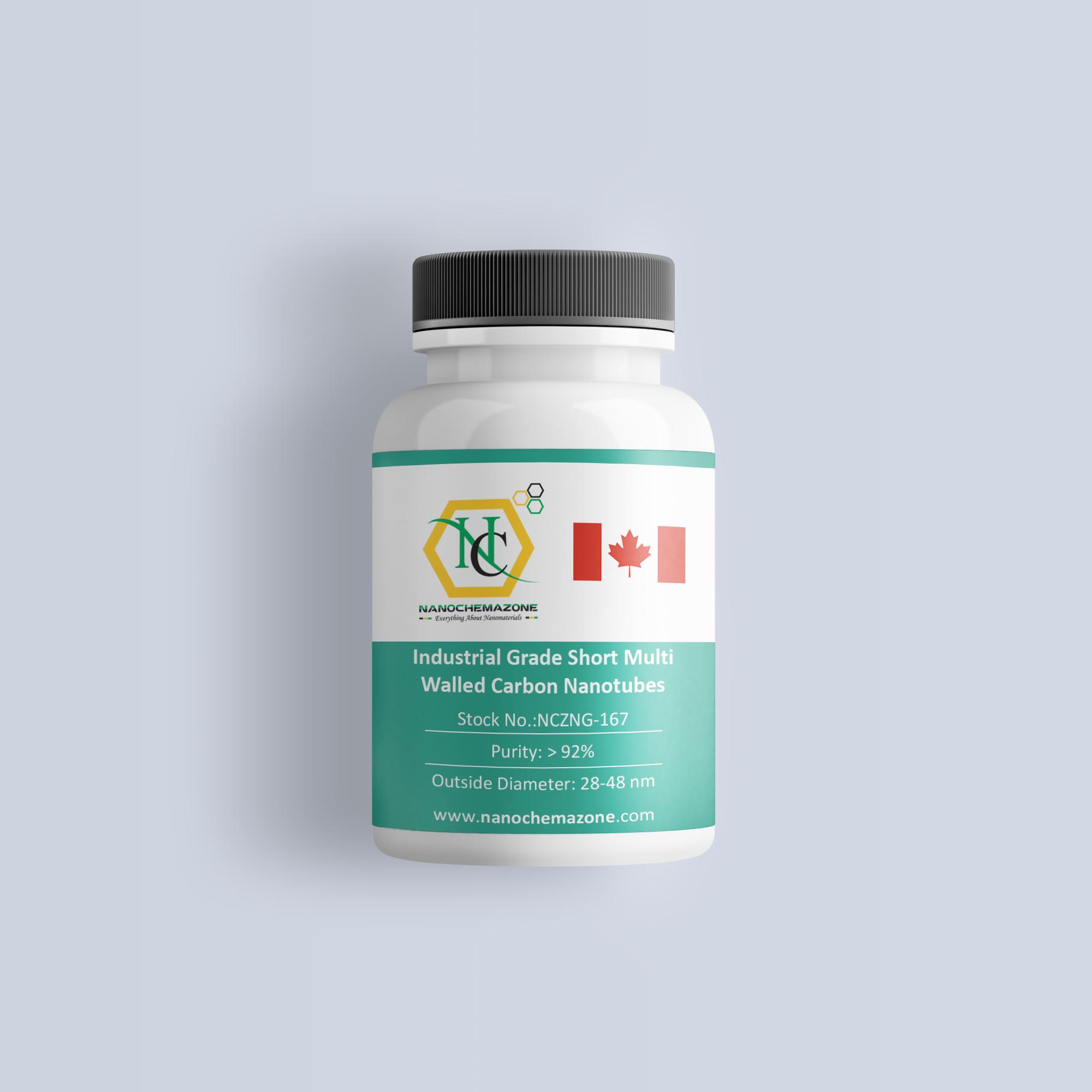
Multi Walled Carbon Nanotubes Water Dispersion
4 wt%, Purity: > 96+ %, OD: 18-28 nm, Length: 8-35 µm
Multi Walled Carbon NanoTubes Water Dispersion is obtained by dispersing MWCNT in deionized water without
the addition of any surfactant. MWCNT water dispersions appear to have great industrial and medical potential.
Dispersion of MWCNT in water is widely used inmass production because of its excellent mechanical and electrical
properties. Our company sells multi walled carbon nanotubes water dispersion with various options.
Technical Properties:
| Purity |
>96+ % |
| Color |
black |
| Average Outside Diameter (nm) |
18-28 |
| Average Inside Diameter (nm) |
5.0-10.0 |
| Length (µm) |
8-35 |
| Tap Density (g/cm3) |
0.30 |
| True Density (g/cm3) |
2.4 |
| Specific Surface Area (m2/g) |
120 |
| Ash |
<1.5 wt% |
| Electrical Conductivity (S/cm) |
>98 |
| Manufacturing Method |
CVD |
Applications:
MWCNTs have a variety of potential applications in different fields. These applications include medicine, mechanical,
electric, chemical, energy and others. It can be applied in drug delivery, biosensors, CNT composites, catalysis,
nanoprobes, hydrogen storage, lithium batteries, gas-discharge tubes, flat panel display, supercapacitor,
transistors, solar cells, photoluminescence, template.