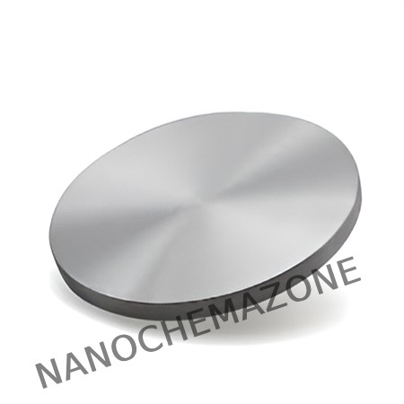
Barium Titanate (BaTiO3) Sputtering Targets, elastomer, Purity: 99.99%, Size: 2”, Thickness: 0.125”

$876.00

Product 

Barium Titanate (BaTiO3) Sputtering Targets, elastomer, Purity: 99.99%, Size: 2'', Thickness: 0.125''

CAS No.

 12047‑27‑7

Appearance

Powder

Purity

≥99%,  ≥99.9%,  ≥95%

(Other purities are also available)

APS

1 – 5 µm (Size Can be customized), Ask for other available size ranges.

Ingredient

N/A

Molecular Weight

~233.19 g/mol

Melting Point

~1625 °C

Boiling Point

N/A

Density

 ~6.02 g/cm³

Product Codes

NCZ-2451K

Praseodymium Calcium Manganate (Pr0.7Ca0.3MnO3) Sputtering Targets, Purity: 99.9%, Size: 1”, Thickness: 0.250”

$878.00

Product 

Praseodymium Calcium Manganate (Pr0.7Ca0.3MnO3) Sputtering Targets, Purity: 99.9%, Size: 1'', Thickness: 0.250''

CAS No.

N/A

Appearance

Powder

Purity

≥99%,  ≥99.9%,  ≥95%

(Other purities are also available)

APS

1–5 μm (Size Can be customized), Ask for other available size ranges.

Ingredient

N/A

Molecular Weight

237.66 g/mol

Melting Point

N/A

Boiling Point

N/A

Density

~6.4–6.8 g/cm³

Product Codes

NCZ-1782K

Lanthanum Titanate (LaTiO3) Sputtering Targets, Purity: 99.9%, Size: 5”, Thickness: 0.125”

$880.00

Applications of Sputtering Targets;

  • Sputtering targets is used for film deposition. The deposition made by sputter targets is a method of depositing thin films by sputtering that involves eroding material from a "target" source onto a "substrate" such as  a silicon wafer.
  • Semiconductor sputtering targets is used to etch the target. Sputter etching is chosen in cases where a high degree of etching anisotropy is needed and selectivity is not a concern.
  • Sputter targets is also used for analysis by etching away the target material.
One of the example occurs in secondary ion spectroscopy (SIMS), where the target sample is sputtered at a constant rate. As the target is sputtered, the concentration and identity of sputtered atoms are measured using mass spectrometry. By helping of the sputtering target, the composition of the target material can be determined and even extremely low concentrations of impurities are detected. Sputtering target has also application area in space. Sputtering is one of the forms of space weathering, a process that changes the physical and chemical properties of airless bodies, such as asteroids and the Moon.

Tin Oxide (SnO2) Sputtering Targets, elastomer, Purity: 99.99%, Size:2”, Thickness: 0.125”

$881.00

Product 

Tin Oxide (SnO2) Sputtering Targets, elastomer, Purity: 99.99%, Size:2'', Thickness: 0.125''

CAS No.

18282-10-5

Appearance

Powder

Purity

≥99%,  ≥99.9%,  ≥95%

(Other purities are also available)

APS

N/A  (Size Can be customized), Ask for other available size ranges.

Ingredient

N/A

Molecular Weight

150.71 g/mol

Melting Point

~1630 °C

Boiling Point

~1800–1900 °C

Density

~6.95 g/cm³

Product Codes

NCZ-1624K

Barium Strontium Titanate (BaO4SrTi) Sputtering Targets, elastomer, Purity: 99.99%, Size: 2”, Thickness: 0.125”

$882.00

Product 

Barium Strontium Titanate (BaO4SrTi) Sputtering Targets, elastomer, Purity: 99.99%, Size: 2'', Thickness: 0.125''

CAS No.

 12060-08-1

Appearance

Powder

Purity

≥99%,  ≥99.9%,  ≥95%

(Other purities are also available)

APS

~1–5 µm (Size Can be customized), Ask for other available size ranges.

Ingredient

N/A

Molecular Weight

~233–300 g/mol (composition dependent)

Melting Point

 ~1625 °C (approximate)

Boiling Point

N/A

Density

~5.5–6.0 g/cm³ (depending on Ba:Sr ratio)

Product Codes

NCZ-2475K

Aluminum Nitride (AlN) Sputtering Targets, elastomer, Purity: 99.8%, Size: 3”, Thickness: 0.125”

$883.00

Applications of Sputtering Targets;

  • Sputtering targets is used for film deposition. The deposition made by sputter targets is a method of depositing thin films by sputtering that involves eroding material from a "target" source onto a "substrate" such as  a silicon wafer.
  • Semiconductor sputtering targets is used to etch the target. Sputter etching is chosen in cases where a high degree of etching anisotropy is needed and selectivity is not a concern.
  • Sputter targets is also used for analysis by etching away the target material.
One of the example occurs in secondary ion spectroscopy (SIMS), where the target sample is sputtered at a constant rate. As the target is sputtered, the concentration and identity of sputtered atoms are measured using mass spectrometry. By helping of the sputtering target, the composition of the target material can be determined and even extremely low concentrations of impurities are detected. Sputtering target has also application area in space. Sputtering is one of the forms of space weathering, a process that changes the physical and chemical properties of airless bodies, such as asteroids and the Moon. Aluminum nitride is a chemical compound with the formula of AlN.Aluminum nitride has excellent combination of physical, chemical, and mechanical properties. High-quality films of aluminum nitride have been used in various devices and sensors including the optical and optoelectronic devices. As far as the optical and optoelectronic applications are concerned, wide band gap (~6.2 eV) along with high-refractive index (~2.0) and low-absorption coefficient (<10−3) makes AlN a very attractive material for these applications. In addition to this, thermal and chemical stability of AlN films make it suitable for applications in difficult environment. Today, AlN films/coatings have been grown by several methods which include pulsed laser deposition, reactive molecular beam epitaxy, vacuum arc/cathodic arc deposition, DC/RF reactive sputtering, ion beam sputtering, metal-organic chemical vapor deposition (MOCVD), and miscellaneous other techniques. Due to simplicity, reproducibility, ease of scaling up, and lower cost, magnetron sputtering is one of the common methods for growing AlN films for various applications. Properties of AlN films depend upon the crystal structure, crystal orientation, microstructure, and chemical composition, which in turn depend upon the deposition conditions such as sputtering power, pulse frequency, duty cycle, growth temperature, nitrogen/argon flow ratio, and sputtering gas pressure. AlN sputtering targets give good result with the method of reactive DC magnetron sputtering system.

Aluminum Nitride (AlN) Sputtering Targets, elastomer, Purity: 99.8%, Size: 3”, Thickness: 0.125”

$883.00

Applications of Sputtering Targets;

For film deposition, sputtering targets are employed. Using a "target" source to erode material onto a "substrate" like a silicon wafer, sputter targets are a technique for depositing thin layers. Targets are etched using semiconductor sputtering targets. When etching anisotropy is required to a great degree and selectivity is not an issue, sputter etching is the method of choice. By etching away the target material, sputter targets are also utilized for investigation. In one instance, the target sample is sputtered at a steady pace in secondary ion spectroscopy (SIMS). Using mass spectrometry, the concentration and identity of the spewed atoms are determined when the target is sputtered. With assistance from the sputtering target, the It is possible to identify the target material and even detect incredibly tiny impurity amounts. There is also an application area for sputtering targets in space. One type of space weathering that alters the chemical and physical characteristics of airless worlds like the Moon and asteroids is sputtering. The chemical compound aluminum nitride has the formula AlN. The combination of mechanical, chemical, and physical properties of aluminum nitride is exceptional. Superior aluminum nitride films have found application in a wide range of sensors and devices, including optoelectronic and optical ones. Regarding optical and optoelectronic applications, AlN is a very desirable material due to its broad band gap (~6.2 eV), high refractive index (~2.0), and low absorption coefficient (<10−3).

Lanthanum Calcium Manganate (La0.7Ca0.3MnO3) Sputtering Targets, Purity: 99.9%, Size: 7”, Thickness: 0.250”

$883.00

Product 

Lanthanum Calcium Manganate (La0.7Ca0.3MnO3) Sputtering Targets, Purity: 99.9%, Size: 7'', Thickness: 0.250''

CAS No.

123273‑09‑6

Appearance

Powder

Purity

≥99%,  ≥99.9%,  ≥95%

(Other purities are also available)

APS

 N/A (Size Can be customized), Ask for other available size ranges.

Ingredient

N/A

Molecular Weight

 ~313.9 g/mol

Melting Point

 ~1,550 °C (approximate; ceramic decomposition likely above)

Boiling Point

N/A

Density

 ~5.3 g/cm³ @ room temp

Product Codes

NCZ-2145K

Aluminum Nitride (AlN) Sputtering Targets, elastomer, Purity: 99.8%, Size: 2”, Thickness: 0.125”

$884.00

Applications of Sputtering Targets;

  • Sputtering targets is used for film deposition. The deposition made by sputter targets is a method of depositing thin films by sputtering that involves eroding material from a "target" source onto a "substrate" such as  a silicon wafer.
  • Semiconductor sputtering targets is used to etch the target. Sputter etching is chosen in cases where a high degree of etching anisotropy is needed and selectivity is not a concern.
  • Sputter targets is also used for analysis by etching away the target material.
One of the example occurs in secondary ion spectroscopy (SIMS), where the target sample is sputtered at a constant rate. As the target is sputtered, the concentration and identity of sputtered atoms are measured using mass spectrometry. By helping of the sputtering target, the composition of the target material can be determined and even extremely low concentrations of impurities are detected. Sputtering target has also application area in space. Sputtering is one of the forms of space weathering, a process that changes the physical and chemical properties of airless bodies, such as asteroids and the Moon. Aluminum nitride is a chemical compound with the formula of AlN.Aluminum nitride has excellent combination of physical, chemical, and mechanical properties. High-quality films of aluminum nitride have been used in various devices and sensors including the optical and optoelectronic devices. As far as the optical and optoelectronic applications are concerned, wide band gap (~6.2 eV) along with high-refractive index (~2.0) and low-absorption coefficient (<10−3) makes AlN a very attractive material for these applications. In addition to this, thermal and chemical stability of AlN films make it suitable for applications in difficult environment. Today, AlN films/coatings have been grown by several methods which include pulsed laser deposition, reactive molecular beam epitaxy, vacuum arc/cathodic arc deposition, DC/RF reactive sputtering, ion beam sputtering, metal-organic chemical vapor deposition (MOCVD), and miscellaneous other techniques. Due to simplicity, reproducibility, ease of scaling up, and lower cost, magnetron sputtering is one of the common methods for growing AlN films for various applications. Properties of AlN films depend upon the crystal structure, crystal orientation, microstructure, and chemical composition, which in turn depend upon the deposition conditions such as sputtering power, pulse frequency, duty cycle, growth temperature, nitrogen/argon flow ratio, and sputtering gas pressure. AlN sputtering targets give good result with the method of reactive DC magnetron sputtering system.

Aluminum Nitride (AlN) Sputtering Targets, elastomer, Purity: 99.8%, Size: 2”, Thickness: 0.125”

$884.00

Applications of Sputtering Targets;

Film deposition is accomplished using sputtering targets. A technique for sputtering thin films is called "deposition made by sputter targets," which entails eroding material from a "target" source onto a "substrate" like a silicon wafer. Etching of the target is done using semiconductor sputtering targets. When selectivity is not an issue and a high degree of etching anisotropy is required, sputter etching is the method of choice. By removing the target material through etching, sputter targets are also utilized for investigation. In secondary ion spectroscopy (SIMS), one example is when the target material is sputtered at a steady pace. Mass spectrometry is used to quantify the concentration and identity of spewed atoms as the target is sputtered. With the sputtering target's assistance, the

It is possible to identify the target material and even detect incredibly tiny impurity amounts.

There is also an application area for sputtering targets in space. One type of space weathering is sputtering, a process that alters the physical and chemical characteristics of bodies without air, such the Moon and asteroids.

Aluminum nitride is a chemical compound with the formula AlN. It possesses a superior blend of mechanical, chemical, and physical properties. attributes. Superior aluminum nitride films have found application in a wide range of sensors and devices, including optoelectronic and optical ones. As Regarding optical and optoelectronic applications, a large band gap (~6.2 eV), a high refractive index (~2.0), and minimal absorption AlN is an extremely appealing material for these applications due to its coefficient (<10−3).

Strontium Titanate (SrTiO3) Sputtering Targets, elastomer, Purity: 99.9%, Size: 1”, Thickness: 0.125”

$884.00

Applications of Sputtering Targets;

Film deposition is accomplished using sputtering targets. A technique for sputtering thin films is called "deposition made by sputter targets," which entails eroding material from a "target" source onto a "substrate" like a silicon wafer. Etching of the target is done using semiconductor sputtering targets. When selectivity is not an issue and a high degree of etching anisotropy is required, sputter etching is the method of choice. By removing the target material through etching, sputter targets are also utilized for investigation. In secondary ion spectroscopy (SIMS), one example is when the target material is sputtered at a steady pace. Mass spectrometry is used to quantify the concentration and identity of spewed atoms as the target is sputtered.

The target material's composition may be ascertained and even very low concentrations of contaminants can be found with the aid of the sputtering target.

There is also an application area for sputtering targets in space. One type of space weathering that alters the chemical and physical characteristics of airless worlds like the Moon and asteroids is sputtering.

Yttrium (Y) Sputtering Targets, Purity: 99.9%, Size: 4”, Thickness: 0.250”

$884.00

Product 

Yttrium (Y) Sputtering Targets, Purity: 99.9%, Size: 4'', Thickness: 0.250''

CAS No.

7440-65-5

Appearance

Powder

Purity

≥99%,  ≥99.9%,  ≥95%

(Other purities are also available)

APS

~20–50 µm*  (Size Can be customized), Ask for other available size ranges.

Ingredient

N/A

Molecular Weight

88.91 g/mol

Melting Point

1522 °C

Boiling Point

3338 °C

Density

4.47 g/cm³

Product Codes

NCZ-1516K

Calcium Manganate (CaMnO3) Sputtering Targets, Purity: 99.9%, Size: 3”, Thickness: 0.125”

$885.00

Product 

Calcium Manganate (CaMnO3) Sputtering Targets, Purity: 99.9%, Size: 3'', Thickness: 0.125''

CAS No.

12058-85-6

Appearance

Powder

Purity

≥99%,  ≥99.9%,  ≥95%

(Other purities are also available)

APS

 N/A (Size Can be customized), Ask for other available size ranges.

Ingredient

N/A

Molecular Weight

157.87 g/mol

Melting Point

 Approx. 1400 °C (decomposes)

Boiling Point

N/A

Density

 ~4.7 g/cm³

Product Codes

NCZ-2359K

Lanthanum Strontium Manganate (La0.9Sr0.1MnO3) Sputtering Targets, indium, Purity: 99.9%, Size: 3”, Thickness: 0.125”

$886.00

Applications of Sputtering Targets;

  • Sputtering targets is used for film deposition. The deposition made by sputter targets is a method of depositing thin films by sputtering that involves eroding material from a "target" source onto a "substrate" such as  a silicon wafer.
  • Semiconductor sputtering targets is used to etch the target. Sputter etching is chosen in cases where a high degree of etching anisotropy is needed and selectivity is not a concern.
  • Sputter targets is also used for analysis by etching away the target material.
One of the example occurs in secondary ion spectroscopy (SIMS), where the target sample is sputtered at a constant rate. As the target is sputtered, the concentration and identity of sputtered atoms are measured using mass spectrometry. By helping of the sputtering target, the composition of the target material can be determined and even extremely low concentrations of impurities are detected. Sputtering target has also application area in space. Sputtering is one of the forms of space weathering, a process that changes the physical and chemical properties of airless bodies, such as asteroids and the Moon.

Molybdenum Disulfide (MoS2) Sputtering Targets, Purity: 99.9%, Size: 4”, Thickness: 0.125”

$886.00

Product 

Molybdenum Disulfide (MoS2) Sputtering Targets, Purity: 99.9%, Size: 4'', Thickness: 0.125''

CAS No.

 1317-33-5

Appearance

Powder

Purity

≥99%,  ≥99.9%,  ≥95%

(Other purities are also available)

APS

 N/A (Size Can be customized), Ask for other available size ranges.

Ingredient

N/A

Molecular Weight

 160.07 g/mol

Melting Point

 ~1185 °C

Boiling Point

 ~4500 °C

Density

 ~5.06 g/cm³

Product Codes

NCZ-1913K

Aluminum Oxide (Al2O3) Sputtering Targets, Purity: 99.99%, Size: 4”, Thickness: 0.250”

$887.00

Product 

Aluminum Oxide (Al2O3) Sputtering Targets, Purity: 99.99%, Size: 4'', Thickness: 0.250''

CAS No.

 1344-28-1

Appearance

Powder

Purity

≥99%,  ≥99.9%,  ≥95%

(Other purities are also available)

APS

N/A (Size Can be customized), Ask for other available size ranges.

Ingredient

N/A

Molecular Weight

101.96 g/mol

Melting Point

~2,072 °C

Boiling Point

~2,977 °C

Density

~3.97–3.98 g/cm³

Product Codes

NCZ-2535K

Lanthanum Titanate (LaTiO3) Sputtering Targets, Purity: 99.9%, Size: 5”, Thickness: 0.250”

$889.00

Applications of Sputtering Targets;

  • Sputtering targets is used for film deposition. The deposition made by sputter targets is a method of depositing thin films by sputtering that involves eroding material from a "target" source onto a "substrate" such as  a silicon wafer.
  • Semiconductor sputtering targets is used to etch the target. Sputter etching is chosen in cases where a high degree of etching anisotropy is needed and selectivity is not a concern.
  • Sputter targets is also used for analysis by etching away the target material.
One of the example occurs in secondary ion spectroscopy (SIMS), where the target sample is sputtered at a constant rate. As the target is sputtered, the concentration and identity of sputtered atoms are measured using mass spectrometry. By helping of the sputtering target, the composition of the target material can be determined and even extremely low concentrations of impurities are detected. Sputtering target has also application area in space. Sputtering is one of the forms of space weathering, a process that changes the physical and chemical properties of airless bodies, such as asteroids and the Moon.

Lanthanum Calcium Manganate (La0.7Ca0.3MnO3) Sputtering Targets, Purity: 99.9%, Size: 8”, Thickness: 0.250”

$893.00

Product 

Lanthanum Calcium Manganate (La0.7Ca0.3MnO3) Sputtering Targets, Purity: 99.9%, Size: 8'', Thickness: 0.250''

CAS No.

123273‑09‑6

Appearance

Powder

Purity

≥99%,  ≥99.9%,  ≥95%

(Other purities are also available)

APS

 N/A (Size Can be customized), Ask for other available size ranges.

Ingredient

N/A

Molecular Weight

 ~313.9 g/mol

Melting Point

 ~1,550 °C (approximate; ceramic decomposition likely above)

Boiling Point

N/A

Density

 ~5.3 g/cm³ @ room temp

Product Codes

NCZ-2143K

Iron Oxide (Fe3O4) Sputtering Targets, Purity: 99.9%, Size: 4”, Thickness: 0.125”

$894.00

Applications of Sputtering Targets;

Film deposition is accomplished using sputtering targets. A technique for sputtering thin films is called "deposition made by sputter targets," which entails eroding material from a "target" source onto a "substrate" like a silicon wafer. Etching of the target is done using semiconductor sputtering targets. When selectivity is not an issue and a high degree of etching anisotropy is required, sputter etching is the method of choice. By removing the target material through etching, sputter targets are also utilized for investigation. In secondary ion spectroscopy (SIMS), one example is when the target material is sputtered at a steady pace. Mass spectrometry is used to quantify the concentration and identity of spewed atoms as the target is sputtered.

The target material's composition may be ascertained and even very low concentrations of contaminants can be found with the aid of the sputtering target.

There is also an application area for sputtering targets in space. One type of space weathering that alters the chemical and physical characteristics of airless worlds like the Moon and asteroids is sputtering.


Manganese (Mn) Sputtering Targets, Purity: 99.95%, Size: 3”, Thickness: 0.250”

$894.00

Applications of Sputtering Targets;

Film deposition is accomplished using sputtering targets. A technique for sputtering thin films is called "deposition made by sputter targets," which entails eroding material from a "target" source onto a "substrate" like a silicon wafer. Etching of the target is done using semiconductor sputtering targets. When selectivity is not an issue and a high degree of etching anisotropy is required, sputter etching is the method of choice. By removing the target material through etching, sputter targets are also utilized for investigation. In secondary ion spectroscopy (SIMS), one example is when the target material is sputtered at a steady pace. Mass spectrometry is used to quantify the concentration and identity of spewed atoms as the target is sputtered.

By helping of the sputtering target, the composition of the target material may be evaluated and even extremely tiny amounts of contaminants are recognized.

There is also an application area for sputtering targets in space. One type of space weathering that alters the chemical and physical characteristics of airless worlds like the Moon and asteroids is sputtering.

Tin Oxide (SnO2) Sputtering Targets, elastomer, Purity: 99.99%, Size: 3”, Thickness: 0.125”

$895.00

Product 

Tin Oxide (SnO2) Sputtering Targets, elastomer, Purity: 99.99%, Size: 3'', Thickness: 0.125''

CAS No.

18282-10-5

Appearance

Powder

Purity

≥99%,  ≥99.9%,  ≥95%

(Other purities are also available)

APS

N/A  (Size Can be customized), Ask for other available size ranges.

Ingredient

N/A

Molecular Weight

150.71 g/mol

Melting Point

~1630 °C

Boiling Point

~1800–1900 °C

Density

~6.95 g/cm³

Product Codes

NCZ-1623K

Indium Oxide (In2O3) Sputtering Targets, Purity: 99.99%, Size: 4”, Thickness: 0.250”

$895.00

Product 

Indium Oxide (In2O3) Sputtering Targets, Purity: 99.99%, Size: 4'', Thickness: 0.250''

CAS No.

 1312-43-2

Appearance

Powder

Purity

≥99%,  ≥99.9%,  ≥95%

(Other purities are also available)

APS

< 5 µm (Size Can be customized), Ask for other available size ranges.

Ingredient

N/A

Molecular Weight

 277.64 g/mol

Melting Point

 ~1,910 °C

Boiling Point

 3,000 °C(approx., decomposes)

Density

~7.18 g/cm³ (sintered form)

Product Codes

NCZ-2213K

Magnesium Oxide (MgO) Sputtering Targets, Purity: 99.95%, Size: 7”, Thickness: 0.125”

$896.00

Applications of Sputtering Targets;

Film deposition is accomplished using sputtering targets. A technique for sputtering thin films is called "deposition made by sputter targets," which entails eroding material from a "target" source onto a "substrate" like a silicon wafer. Etching of the target is done using semiconductor sputtering targets. When selectivity is not an issue and a high degree of etching anisotropy is required, sputter etching is the method of choice. By removing the target material through etching, sputter targets are also utilized for investigation. In secondary ion spectroscopy (SIMS), one example is when the target material is sputtered at a steady pace. Mass spectrometry is used to quantify the concentration and identity of spewed atoms as the target is sputtered.

The target material's composition may be ascertained and even very low concentrations of contaminants can be found with the aid of the sputtering target.

There is also an application area for sputtering targets in space. One type of space weathering that alters the chemical and physical characteristics of airless worlds like the Moon and asteroids is sputtering.

Lithium Niobate (LiNbO3) Sputtering Targets, Purity: 99.9%, Size: 4”, Thickness: 0.125”

$897.00

Applications of Sputtering Targets;

Film deposition is accomplished using sputtering targets. A technique for sputtering thin films is called "deposition made by sputter targets," which entails eroding material from a "target" source onto a "substrate" like a silicon wafer. Etching of the target is done using semiconductor sputtering targets. When selectivity is not an issue and a high degree of etching anisotropy is required, sputter etching is the method of choice. By removing the target material through etching, sputter targets are also utilized for investigation. In secondary ion spectroscopy (SIMS), one example is when the target material is sputtered at a steady pace. Mass spectrometry is used to quantify the concentration and identity of spewed atoms as the target is sputtered.

By helping of the sputtering target, the composition of the target material may be evaluated and even extremely tiny amounts of contaminants are recognized.

There is also an application area for sputtering targets in space. One type of space weathering that alters the chemical and physical characteristics of airless worlds like the Moon and asteroids is sputtering.

Titanium Carbide (TiC) Sputtering Targets, Purity: 99.5%, Size: 3”, Thickness: 0.250”

$897.00

Product 

Titanium Carbide (TiC) Sputtering Targets, Purity: 99.5%, Size: 3'', Thickness: 0.250''

CAS No.

 12070-08-5

Appearance

Powder

Purity

≥99%,  ≥99.9%,  ≥95%

(Other purities are also available)

APS

N/A  (Size Can be customized), Ask for other available size ranges.

Ingredient

N/A

Molecular Weight

59.89 g/mol

Melting Point

 ~3160 °C

Boiling Point

N/A

Density

4.93 g/cm³

Product Codes

NCZ-1609K

Tungsten Oxide (WO3) Sputtering Targets, Purity: 99.9%, Size: 1”, Thickness: 0.250”

$899.00

Product 

Tungsten Oxide (WO3) Sputtering Targets, Purity: 99.9%, Size: 1'', Thickness: 0.250''

CAS No.

1314-35-8

Appearance

Powder

Purity

≥99%,  ≥99.9%,  ≥95%

(Other purities are also available)

APS

N/A  (Size Can be customized), Ask for other available size ranges.

Ingredient

N/A

Molecular Weight

231.84 g/mol

Melting Point

1,473 °C

Boiling Point

1,700–1,850 °C

Density

7.16 g/cm³

Product Codes

NCZ-1573K

Magnesium Fluoride (MgF2) Sputtering Targets, Purity: 99.9%, Size: 6”, Thickness: 0.250”

$899.00

Product 

Magnesium Fluoride (MgF2) Sputtering Targets, Purity: 99.9%, Size: 6'', Thickness: 0.250''

CAS No.

7783-40-6

Appearance

Powder

Purity

≥99%,  ≥99.9%,  ≥95%

(Other purities are also available)

APS

 N/A (Size Can be customized), Ask for other available size ranges.

Ingredient

N/A

Molecular Weight

 62.30 g/mol

Melting Point

~1263 °C

Boiling Point

~2260 °C

Density

 3.18 g/cm³

Product Codes

NCZ-1978K

Iron Oxide (Fe3O4) Sputtering Targets, Purity: 99.9%, Size: 5”, Thickness: 0.250”

$900.00

Applications of Sputtering Targets;

Film deposition is accomplished using sputtering targets. A technique for sputtering thin films is called "deposition made by sputter targets," which entails eroding material from a "target" source onto a "substrate" like a silicon wafer. Etching of the target is done using semiconductor sputtering targets. When selectivity is not an issue and a high degree of etching anisotropy is required, sputter etching is the method of choice. By removing the target material through etching, sputter targets are also utilized for investigation. In secondary ion spectroscopy (SIMS), one example is when the target material is sputtered at a steady pace. Mass spectrometry is used to quantify the concentration and identity of spewed atoms as the target is sputtered.

The target material's composition may be ascertained and even very low concentrations of contaminants can be found with the aid of the sputtering target.

There is also an application area for sputtering targets in space. One type of space weathering that alters the chemical and physical characteristics of airless worlds like the Moon and asteroids is sputtering.

Yttrium Ferrite (Y3Fe5O12) Sputtering Targets, Purity: 99.9%, Size: 1”, Thickness: 0.125”

$900.00

Product 

Yttrium Ferrite (Y3Fe5O12) Sputtering Targets, Purity: 99.9%, Size: 1'', Thickness: 0.125''

CAS No.

12063-56-8

Appearance

Powder

Purity

≥99%,  ≥99.9%,  ≥95%

(Other purities are also available)

APS

~2–10 µm (Size Can be customized), Ask for other available size ranges.

Ingredient

N/A

Molecular Weight

737.94 g/mol

Melting Point

~1040–1550 °C

Boiling Point

N/A

Density

~5.11 g/cm³

Product Codes

NCZ-1515K

Iron Oxide (Fe3O4) Sputtering Targets, indium, Purity: 99.9%, Size: 2”, Thickness: 0.125”

$900.00

Product 

Iron Oxide (Fe3O4) Sputtering Targets, indium, Purity: 99.9%, Size: 2'', Thickness: 0.125''

CAS No.

1317‑61‑9

Appearance

Powder

Purity

≥99%,  ≥99.9%,  ≥95%

(Other purities are also available)

APS

 N/A (Size Can be customized), Ask for other available size ranges.

Ingredient

N/A

Molecular Weight

 231.6 g/mol

Melting Point

~1,597 °C

Boiling Point

 ~2,623 °C (material may decompose before boiling)

Density

 ~5.17 g/cm³ (sintered target)

Product Codes

NCZ-2162K

Tin Oxide (SnO2) Sputtering Targets, elastomer, Purity: 99.99%, Size: 4”, Thickness: 0.125”

$902.00

Product 

Tin Oxide (SnO2) Sputtering Targets, elastomer, Purity: 99.99%, Size: 4'', Thickness: 0.125''

CAS No.

18282-10-5

Appearance

Powder

Purity

≥99%,  ≥99.9%,  ≥95%

(Other purities are also available)

APS

N/A  (Size Can be customized), Ask for other available size ranges.

Ingredient

N/A

Molecular Weight

150.71 g/mol

Melting Point

~1630 °C

Boiling Point

~1800–1900 °C

Density

~6.95 g/cm³

Product Codes

NCZ-1622K

Tantalum (Ta) Sputtering Targets, Purity: 99.95%, Size: 6”, Thickness: 0.250”

$902.00

Product 

Tantalum (Ta) Sputtering Targets, Purity: 99.95%, Size: 6'', Thickness: 0.250''

CAS No.

 7440-25-7

Appearance

Powder

Purity

≥99%,  ≥99.9%,  ≥95%

(Other purities are also available)

APS

N/A  (Size Can be customized), Ask for other available size ranges.

Ingredient

N/A

Molecular Weight

 180.95 g/mol

Melting Point

3017 °C

Boiling Point

 5458 °C

Density

16.65 g/cm³

Product Codes

NCZ-1659K

Strontium Titanate (SrTiO3) Sputtering Targets, Purity: 99.9%, Size: 7”, Thickness: 0.250”

$902.00

Product 

Strontium Titanate (SrTiO3) Sputtering Targets, Purity: 99.9%, Size: 7'', Thickness: 0.250''

CAS No.

12060-08-1

Appearance

Powder

Purity

≥99%,  ≥99.9%,  ≥95%

(Other purities are also available)

APS

N/A  (Size Can be customized), Ask for other available size ranges.

Ingredient

N/A

Molecular Weight

183.49 g/mol

Melting Point

 ~2080 °C

Boiling Point

N/A

Density

~5.12 g/cm³

Product Codes

NCZ-1671K

Titanium Nitride (TiN) Sputtering Targets, indium, Purity: 99.5%, Size: 2”, Thickness: 0.125”

$905.00

Product 

Titanium Nitride (TiN) Sputtering Targets, indium, Purity: 99.5%, Size: 2'', Thickness: 0.125''

CAS No.

25583-20-4

Appearance

Powder

Purity

≥99%,  ≥99.9%,  ≥95%

(Other purities are also available)

APS

N/A  (Size Can be customized), Ask for other available size ranges.

Ingredient

N/A

Molecular Weight

61.88 g/mol

Melting Point

 ~2950 °C

Boiling Point

~4300 °C

Density

5.22 g/cm³

Product Codes

NCZ-1599K

Zinc Oxide (ZnO) Sputtering Targets, indium, Purity: 99.99%, Size: 2”, Thickness: 0.125”

$906.00

Product 

Zinc Oxide (ZnO) Sputtering Targets, indium, Purity: 99.99%, Size: 2'', Thickness: 0.125''

CAS No.

1314-13-2

Appearance

Powder

Purity

≥99%,  ≥99.9%,  ≥95%

(Other purities are also available)

APS

 (ZnO) (Size Can be customized), Ask for other available size ranges.

Ingredient

N/A

Molecular Weight

81.38 g/mol

Melting Point

1975 °C

Boiling Point

N/A

Density

5.61 g/cm³

Product Codes

NCZ-1496K

Lithium Cobalt Oxide (LiCoO2) Sputtering Targets, indium, Purity: 99.9%, Size: 2”, Thickness: 0.125”

$906.00

Product 

Lithium Cobalt Oxide (LiCoO2) Sputtering Targets, indium, Purity: 99.9%, Size: 2'', Thickness: 0.125''

CAS No.

12190‑79‑3

Appearance

Powder

Purity

≥99%,  ≥99.9%,  ≥95%

(Other purities are also available)

APS

 N/A (Size Can be customized), Ask for other available size ranges.

Ingredient

N/A

Molecular Weight

97.87 g/mol

Melting Point

~1,130 °C

Boiling Point

N/A

Density

~4.95 g/cm³

Product Codes

NCZ-2047K

Iron Oxide (Fe3O4) Sputtering Targets, Purity: 99.9%, Size: 4”, Thickness: 0.250”

$906.00

Product 

Iron Oxide (Fe3O4) Sputtering Targets, Purity: 99.9%, Size: 4'', Thickness: 0.250''

CAS No.

1317‑61‑9

Appearance

Powder

Purity

≥99%,  ≥99.9%,  ≥95%

(Other purities are also available)

APS

 N/A (Size Can be customized), Ask for other available size ranges.

Ingredient

N/A

Molecular Weight

 231.6 g/mol

Melting Point

~1,597 °C

Boiling Point

 ~2,623 °C (material may decompose before boiling)

Density

 ~5.17 g/cm³ (sintered target)

Product Codes

NCZ-2170K

Barium Zirconate (BaZrO3) Sputtering Targets, Purity: 99.99%, Size: 3”, Thickness: 0.125”

$907.00

Applications of Sputtering Targets;

Film deposition is accomplished using sputtering targets. A technique for sputtering thin films is called "deposition made by sputter targets," which entails eroding material from a "target" source onto a "substrate" like a silicon wafer. Etching of the target is done using semiconductor sputtering targets. When selectivity is not an issue and a high degree of etching anisotropy is required, sputter etching is the method of choice. By removing the target material through etching, sputter targets are also utilized for investigation. In secondary ion spectroscopy (SIMS), one example is when the target material is sputtered at a steady pace. Mass spectrometry is used to quantify the concentration and identity of spewed atoms as the target is sputtered. With the sputtering target's assistance, the

It is possible to identify the target material and even detect incredibly tiny impurity amounts.

There is also an application area for sputtering targets in space. One type of space weathering that alters the chemical and physical characteristics of airless worlds like the Moon and asteroids is sputtering.

The chemical compound barium zirconate has the formula BaZrO3. An electroceramic, or family of ceramic materials principally employed for their electrical capabilities, is what barium zirconate is. In semiconductor, chemical vapor deposition (CVD), physical vapor deposition (PVD), and optical applications, barium zirconate sputtering targets can be employed. Barium zirconate sputtering targets can also be employed for ferroelectric applications.

Strontium Titanate (SrTiO3) Sputtering Targets, Purity: 99.9%, Size: 6”, Thickness: 0.125”

$907.00

Product 

Strontium Titanate (SrTiO3) Sputtering Targets, Purity: 99.9%, Size: 6'', Thickness: 0.125''

CAS No.

12060-08-1

Appearance

Powder

Purity

≥99%,  ≥99.9%,  ≥95%

(Other purities are also available)

APS

N/A  (Size Can be customized), Ask for other available size ranges.

Ingredient

N/A

Molecular Weight

183.49 g/mol

Melting Point

 ~2080 °C

Boiling Point

N/A

Density

~5.12 g/cm³

Product Codes

NCZ-1674K

Strontium Titanate (SrTiO3) Sputtering Targets, elastomer, Purity: 99.9%, Size: 2”, Thickness: 0.125”

$909.00

Applications of Sputtering Targets;

Film deposition is accomplished using sputtering targets. A technique for sputtering thin films is called "deposition made by sputter targets," which entails eroding material from a "target" source onto a "substrate" like a silicon wafer. Etching of the target is done using semiconductor sputtering targets. When selectivity is not an issue and a high degree of etching anisotropy is required, sputter etching is the method of choice. By removing the target material through etching, sputter targets are also utilized for investigation. In secondary ion spectroscopy (SIMS), one example is when the target material is sputtered at a steady pace. Mass spectrometry is used to quantify the concentration and identity of spewed atoms as the target is sputtered.

The target material's composition may be ascertained and even very low concentrations of contaminants can be found with the aid of the sputtering target.

There is also an application area for sputtering targets in space. One type of space weathering that alters the chemical and physical characteristics of airless worlds like the Moon and asteroids is sputtering.

Titanium Dioxide (TiO2) Sputtering Targets, indium, Purity: 99.95%, Size: 4”, Thickness: 0.125” , Grey to Black

$909.00

Applications of Sputtering Targets;

Film deposition is accomplished using sputtering targets. A technique for sputtering thin films is called "deposition made by sputter targets," which entails eroding material from a "target" source onto a "substrate" like a silicon wafer. Etching of the target is done using semiconductor sputtering targets. When selectivity is not an issue and a high degree of etching anisotropy is required, sputter etching is the method of choice. By removing the target material through etching, sputter targets are also utilized for investigation. In secondary ion spectroscopy (SIMS), one example is when the target material is sputtered at a steady pace. Mass spectrometry is used to quantify the concentration and identity of spewed atoms as the target is sputtered.

The target material's composition may be ascertained and even very low concentrations of contaminants can be found with the aid of the sputtering target.

There is also an application area for sputtering targets in space. One type of space weathering that alters the chemical and physical characteristics of airless worlds like the Moon and asteroids is sputtering.

Yttrium Ferrite (Y3Fe5O12) Sputtering Targets, Purity: 99.9%, Size: 1”, Thickness: 0.250”

$909.00

Product 

Yttrium Ferrite (Y3Fe5O12) Sputtering Targets, Purity: 99.9%, Size: 1'', Thickness: 0.250''

CAS No.

12068-40-5

Appearance

Powder

Purity

≥99%,  ≥99.9%,  ≥95%

(Other purities are also available)

APS

 N/A (Size Can be customized), Ask for other available size ranges.

Ingredient

N/A

Molecular Weight

706.32 g/mol

Melting Point

~1,790 °C

Boiling Point

N/A

Density

~5.17 – 5.36

Product Codes

NCZ-1514K

Cerium Oxide (CeO2) Sputtering Targets, Purity: 99.99%, Size: 2”, Thickness: 0.250”

$909.00

Product 

Cerium Oxide (CeO2) Sputtering Targets, Purity: 99.99%, Size: 2'', Thickness: 0.250''

CAS No.

 1306-38-3

Appearance

Powder

Purity

≥99%,  ≥99.9%,  ≥95%

(Other purities are also available)

APS

 N/A (Size Can be customized), Ask for other available size ranges.

Ingredient

N/A

Molecular Weight

 172.11 g/mol

Melting Point

2,400–2,600 °C

Boiling Point

Sublimes above 3,000 °C

Density

 7.13 g/cm³

Product Codes

NCZ-2332K

Lanthanum Manganate (LaMnO3) Sputtering Targets, Purity: 99.9%, Size: 5”, Thickness: 0.250”

$910.00

Applications of Sputtering Targets;

Film deposition is accomplished using sputtering targets. A technique for sputtering thin films is called "deposition made by sputter targets," which entails eroding material from a "target" source onto a "substrate" like a silicon wafer. Etching of the target is done using semiconductor sputtering targets. When selectivity is not an issue and a high degree of etching anisotropy is required, sputter etching is the method of choice. By removing the target material through etching, sputter targets are also utilized for investigation. In secondary ion spectroscopy (SIMS), one example is when the target material is sputtered at a steady pace. Mass spectrometry is used to quantify the concentration and identity of spewed atoms as the target is sputtered.

The target material's composition may be ascertained and even very low concentrations of contaminants can be found with the aid of the sputtering target.

There is also an application area for sputtering targets in space. One type of space weathering that alters the chemical and physical characteristics of airless worlds like the Moon and asteroids is sputtering.

Manganese (Mn) Sputtering Targets, Purity: 99.95%, Size: 3”, Thickness: 0.125”

$910.00

Product 

Manganese (Mn) Sputtering Targets, Purity: 99.95%, Size: 3'', Thickness: 0.125''

CAS No.

 7439-96-5

Appearance

Powder

Purity

≥99%,  ≥99.9%,  ≥95%

(Other purities are also available)

APS

 N/A (Size Can be customized), Ask for other available size ranges.

Ingredient

N/A

Molecular Weight

54.93804 g/mol

Melting Point

 1,246 °C

Boiling Point

 2,061 °C

Density

 7.21 g/cm³

Product Codes

NCZ-1950K

Lithium Phosphate (Li3PO4) Sputtering Targets, elastomer, Purity: 99.95%, Size: 1”, Thickness: 0.125”

$913.00

Product 

Lithium Phosphate (Li3PO4) Sputtering Targets, elastomer, Purity: 99.95%, Size: 1'', Thickness: 0.125''

CAS No.

10377-52-3

Appearance

Powder

Purity

≥99%,  ≥99.9%,  ≥95%

(Other purities are also available)

APS

 N/A (Size Can be customized), Ask for other available size ranges.

Ingredient

N/A

Molecular Weight

 115.79 g/mol

Melting Point

 ~837 °C

Boiling Point

N/A

Density

 ~2.53 g/cm³

Product Codes

NCZ-2019K

Lithium Cobalt Oxide (LiCoO2) Sputtering Targets, Purity: 99.9%, Size: 3”, Thickness: 0.250”

$914.00

Product 

Lithium Cobalt Oxide (LiCoO2) Sputtering Targets, Purity: 99.9%, Size: 3'', Thickness: 0.250''

CAS No.

12190‑79‑3

Appearance

Powder

Purity

≥99%,  ≥99.9%,  ≥95%

(Other purities are also available)

APS

 N/A (Size Can be customized), Ask for other available size ranges.

Ingredient

N/A

Molecular Weight

97.87 g/mol

Melting Point

 ~1,100–1,130 °C (decomposes rather than boils)

Boiling Point

N/A

Density

~4.80–4.95 g/cm³

Product Codes

NCZ-2050K

Germanium (Ge) Sputtering Targets, indium, Purity: 99.999%, Size: 3”, Thickness: 0.125”

$914.00

Product 

Germanium (Ge) Sputtering Targets, indium, Purity: 99.999%, Size: 3'', Thickness: 0.125''

CAS No.

7440-56-4

Appearance

Powder

Purity

≥99%,  ≥99.9%,  ≥95%

(Other purities are also available)

APS

 N/A (Size Can be customized), Ask for other available size ranges.

Ingredient

N/A

Molecular Weight

 72.63 g/mol

Melting Point

 938.3 °C

Boiling Point

2,833 °C

Density

 5.32 g/cm³

Product Codes

NCZ-2235K

Aluminum Nitride (AlN) Sputtering Targets, Purity: 99.8%, Size: 2”, Thickness: 0.250”

$914.00

Product 

Aluminum Nitride (AlN) Sputtering Targets, Purity: 99.8%, Size: 2'', Thickness: 0.250''

CAS No.

 24304-00-5

Appearance

Powder

Purity

≥99%,  ≥99.9%,  ≥95%

(Other purities are also available)

APS

N/A (Size Can be customized), Ask for other available size ranges.

Ingredient

N/A

Molecular Weight

40.99 g/mol

Melting Point

 ~2200 °C

Boiling Point

 N/A

Density

 ~3.26 g/cm³

Product Codes

NCZ-2558K

Vanadium Oxide (V2O5) Sputtering Targets, elastomer, Purity: 99.9%, Size: 4”, Thickness: 0.125”

$919.00

Applications of Sputtering Targets;

Film deposition is accomplished using sputtering targets. A technique for sputtering thin films is called "deposition made by sputter targets," which entails eroding material from a "target" source onto a "substrate" like a silicon wafer. Etching of the target is done using semiconductor sputtering targets. When selectivity is not an issue and a high degree of etching anisotropy is required, sputter etching is the method of choice. By removing the target material through etching, sputter targets are also utilized for investigation. In secondary ion spectroscopy (SIMS), one example is when the target material is sputtered at a steady pace. Mass spectrometry is used to quantify the concentration and identity of spewed atoms as the target is sputtered.

The target material's composition may be ascertained and even very low concentrations of contaminants can be found with the aid of the sputtering target.

There is also an application area for sputtering targets in space. One type of space weathering that alters the chemical and physical characteristics of airless worlds like the Moon and asteroids is sputtering.

Iron Oxide (Fe3O4) Sputtering Targets, Purity: 99.9%, Size: 6”, Thickness: 0.125”

$921.00

Applications of Sputtering Targets;

Film deposition is accomplished using sputtering targets. A technique for sputtering thin films is called "deposition made by sputter targets," which entails eroding material from a "target" source onto a "substrate" like a silicon wafer. Etching of the target is done using semiconductor sputtering targets. When selectivity is not an issue and a high degree of etching anisotropy is required, sputter etching is the method of choice. By removing the target material through etching, sputter targets are also utilized for investigation. In secondary ion spectroscopy (SIMS), one example is when the target material is sputtered at a steady pace. Mass spectrometry is used to quantify the concentration and identity of spewed atoms as the target is sputtered.

The target material's composition may be ascertained and even very low concentrations of contaminants can be found with the aid of the sputtering target.

There is also an application area for sputtering targets in space. One type of space weathering that alters the chemical and physical characteristics of airless worlds like the Moon and asteroids is sputtering.

Bismuth Ferrite (BiFeO3) Sputtering Targets, Purity: 99.9%, Size: 2”, Thickness: 0.250”

$924.00

Applications of Sputtering Targets;

Film deposition is accomplished using sputtering targets. A technique for sputtering thin films is called "deposition made by sputter targets," which entails eroding material from a "target" source onto a "substrate" like a silicon wafer. Etching of the target is done using semiconductor sputtering targets. When selectivity is not an issue and a high degree of etching anisotropy is required, sputter etching is the method of choice. By removing the target material through etching, sputter targets are also utilized for investigation. In secondary ion spectroscopy (SIMS), one example is when the target material is sputtered at a steady pace. Mass spectrometry is used to quantify the concentration and identity of spewed atoms as the target is sputtered. With the sputtering target's assistance, the

There is also an application area for sputtering targets in space. One type of space weathering that alters the chemical and physical characteristics of airless worlds like the Moon and asteroids is sputtering.

One of the most promising multiferroic materials is bismuth ferrite, an inorganic chemical compound with a perovskite structure and the chemical formula BiFeO3. In order to create a one-phase material called bismuth ferrite (BiFeO3), a bismuth ferrite sputtering target is often manufactured by high temperature sinttering or recrystallizing the mixture of the oxide compound of Bi and Fe. For targets that are sputtering bismuth ferrite, indium bonding is advised.

Scandium (Sc) Sputtering Target

Price range: $927.00 through $2,148.00
Select options This product has multiple variants. The options may be chosen on the product page

Product 

Scandium (Sc) Sputtering Target

CAS No.

7440-20-2

Appearance

Powder

Purity

≥99%,  ≥99.9%,  ≥95%

(Other purities are also available)

APS

 NA (Size Can be customized), Ask for other available size ranges.

Ingredient

N/A

Molecular Weight

44.96 g/mol

Melting Point

 1,541 °C

Boiling Point

 2,838 °C

Density

2.99 g/cm³

Product Codes

NCZ-1359K

Carbon (C) (Pyrolytic Graphite) Sputtering Targets, indium, Purity: 99.999%, Size: 3”, Thickness: 0.125”

$927.00

Product 

Carbon (C) (Pyrolytic Graphite) Sputtering Targets, indium, Purity: 99.999%, Size: 3'', Thickness: 0.125''

CAS No.

 7782-42-5

Appearance

Powder

Purity

≥99%,  ≥99.9%,  ≥95%

(Other purities are also available)

APS

 N/A (Size Can be customized), Ask for other available size ranges.

Ingredient

N/A

Molecular Weight

 12.01 g/mol

Melting Point

Sublimes at ~3,600 °C (does not melt under normal pressure)

Boiling Point

 Sublimes directly without boiling phase at ~3,600 °C+

Density

~2.2 g/cm³ (varies with crystallinity and orientation)

Product Codes

NCZ-2335K

Titanium Dioxide (TiO2) Sputtering Targets, indium, Purity: 99.9%, Size: 3”, Thickness: 0.125”, Grey to Black

$928.00

Applications of Sputtering Targets;

Film deposition is accomplished using sputtering targets. A technique for sputtering thin films is called "deposition made by sputter targets," which entails eroding material from a "target" source onto a "substrate" like a silicon wafer. Etching of the target is done using semiconductor sputtering targets. When selectivity is not an issue and a high degree of etching anisotropy is required, sputter etching is the method of choice. By removing the target material through etching, sputter targets are also utilized for investigation. In secondary ion spectroscopy (SIMS), one example is when the target material is sputtered at a steady pace. Mass spectrometry is used to quantify the concentration and identity of spewed atoms as the target is sputtered.

The target material's composition may be ascertained and even very low concentrations of contaminants can be found with the aid of the sputtering target.

There is also an application area for sputtering targets in space. One type of space weathering that alters the chemical and physical characteristics of airless worlds like the Moon and asteroids is sputtering.

Titanium Nitride (TiN) Sputtering Targets, Purity: 99.5%, Size: 4”, Thickness: 0.125”

$930.00

Applications of Sputtering Targets;

Film deposition is accomplished using sputtering targets. A technique for sputtering thin films is called "deposition made by sputter targets," which entails eroding material from a "target" source onto a "substrate" like a silicon wafer. Etching of the target is done using semiconductor sputtering targets. When selectivity is not an issue and a high degree of etching anisotropy is required, sputter etching is the method of choice. By removing the target material through etching, sputter targets are also utilized for investigation. In secondary ion spectroscopy (SIMS), one example is when the target material is sputtered at a steady pace. Mass spectrometry is used to quantify the concentration and identity of spewed atoms as the target is sputtered.

The target material's composition may be ascertained and even very low concentrations of contaminants can be found with the aid of the sputtering target.

There is also an application area for sputtering targets in space. One type of space weathering that alters the chemical and physical characteristics of airless worlds like the Moon and asteroids is sputtering.

Zinc Oxide (ZnO) Sputtering Targets, indium, Purity: 99.9%, Size: 3”, Thickness: 0.125”

$930.00

Applications of Sputtering Targets;

Film deposition is accomplished using sputtering targets. A technique for sputtering thin films is called "deposition made by sputter targets," which entails eroding material from a "target" source onto a "substrate" like a silicon wafer. Etching of the target is done using semiconductor sputtering targets. When selectivity is not an issue and a high degree of etching anisotropy is required, sputter etching is the method of choice. By removing the target material through etching, sputter targets are also utilized for investigation. In secondary ion spectroscopy (SIMS), one example is when the target material is sputtered at a steady pace. Mass spectrometry is used to quantify the concentration and identity of spewed atoms as the target is sputtered.

The target material's composition may be ascertained and even very low concentrations of contaminants can be found with the aid of the sputtering target.

There is also an application area for sputtering targets in space. One type of space weathering that alters the chemical and physical characteristics of airless worlds like the Moon and asteroids is sputtering.

Lead Zirconium Titanate/PZT (O5PbTiZr) Sputtering Targets, Purity: 99.9%, Size: 2”, Thickness: 0.125”

$931.00

Applications of Sputtering Targets;

Film deposition is accomplished using sputtering targets. A technique for sputtering thin films is called "deposition made by sputter targets," which entails eroding material from a "target" source onto a "substrate" like a silicon wafer. Etching of the target is done using semiconductor sputtering targets. When selectivity is not an issue and a high degree of etching anisotropy is required, sputter etching is the method of choice. By removing the target material through etching, sputter targets are also utilized for investigation. In secondary ion spectroscopy (SIMS), one example is when the target material is sputtered at a steady pace. Mass spectrometry is used to quantify the concentration and identity of spewed atoms as the target is sputtered.

By helping of the sputtering target, the composition of the target material may be evaluated and even extremely tiny amounts of contaminants are recognized.

There is also an application area for sputtering targets in space. One type of space weathering that alters the chemical and physical characteristics of airless worlds like the Moon and asteroids is sputtering.

An inorganic substance is lead zirconium titanate. This ceramic perovskite material has a strong piezoelectric effect, which means that when an electric field is applied, the compound changes shape. Lead zirconium titanate is employed in a number of practical applications such as ultrasonic transducers and piezoelectric resonators.

Bismuth Telluride (Bi2Te3) Sputtering Targets, Purity: 99.999%, Size: 2”, Thickness: 0.125”

$931.00

Product 

Bismuth Telluride (Bi2Te3) Sputtering Targets, Purity: 99.999%, Size: 2'', Thickness: 0.125''

CAS No.

 1304-82-1

Appearance

Powder

Purity

≥99%,  ≥99.9%,  ≥95%

(Other purities are also available)

APS

 N/A (Size Can be customized), Ask for other available size ranges.

Ingredient

N/A

Molecular Weight

800.55 g/mol

Melting Point

~585 °C

Boiling Point

~987 °C (sublimes)

Density

 ~7.7 g/cm³

Product Codes

NCZ-2401K

Strontium Titanate (SrTiO3) Sputtering Targets, Purity: 99.9%, Size: 5”, Thickness: 0.125”

$932.00

Product 

Strontium Titanate (SrTiO3) Sputtering Targets, Purity: 99.9%, Size: 5'', Thickness: 0.125''

CAS No.

12060-08-1

Appearance

Powder

Purity

≥99%,  ≥99.9%,  ≥95%

(Other purities are also available)

APS

N/A  (Size Can be customized), Ask for other available size ranges.

Ingredient

N/A

Molecular Weight

183.49 g/mol

Melting Point

 ~2080 °C

Boiling Point

N/A

Density

~5.12 g/cm³

Product Codes

NCZ-1676K