Barium Titanate (BaTiO3) Sputtering Targets, elastomer, Purity: 99.99%, Size: 1”, Thickness: 0.125”

$831.00

Product 

Barium Titanate (BaTiO3) Sputtering Targets, elastomer, Purity: 99.99%, Size: 1'', Thickness: 0.125''

CAS No.

 12047‑27‑7

Appearance

Powder

Purity

≥99%,  ≥99.9%,  ≥95%

(Other purities are also available)

APS

1 – 5 µm (Size Can be customized), Ask for other available size ranges.

Ingredient

N/A

Molecular Weight

~233.19 g/mol

Melting Point

~1625 °C

Boiling Point

N/A

Density

 ~6.02 g/cm³

Product Codes

NCZ-2452K

Tantalum (Ta) Sputtering Targets, Purity: 99.95%, Size: 4”, Thickness: 0.125”

$832.00

Product 

Tantalum (Ta) Sputtering Targets, Purity: 99.95%, Size: 4'', Thickness: 0.125''

CAS No.

 7440-25-7

Appearance

Powder

Purity

≥99%,  ≥99.9%,  ≥95%

(Other purities are also available)

APS

N/A  (Size Can be customized), Ask for other available size ranges.

Ingredient

N/A

Molecular Weight

 180.95 g/mol

Melting Point

3017 °C

Boiling Point

 5458 °C

Density

16.65 g/cm³

Product Codes

NCZ-1661K

Lanthanum Titanate (LaTiO3) Sputtering Targets, Purity: 99.9%, Size: 2”, Thickness: 0.250”

$832.00

Product 

Lanthanum Titanate (LaTiO3) Sputtering Targets, Purity: 99.9%, Size: 2'', Thickness: 0.250''

CAS No.

 12201-04-6

Appearance

Powder

Purity

≥99%,  ≥99.9%,  ≥95%

(Other purities are also available)

APS

<5 µm (Size Can be customized), Ask for other available size ranges.

Ingredient

N/A

Molecular Weight

 234.77 g/mol (exact ~234.839 g/mol)

Melting Point

 Approx. 2,200 °C

Boiling Point

N/A

Density

N/A

Product Codes

NCZ-2091K

Lanthanum Aluminate (LaAlO3) Sputtering Targets, indium, Purity: 99.9%, Size: 2”, Thickness: 0.125”

$833.00

Applications of Sputtering Targets;

Film deposition is accomplished using sputtering targets. A technique for sputtering thin films is called "deposition made by sputter targets," which entails eroding material from a "target" source onto a "substrate" like a silicon wafer. Etching of the target is done using semiconductor sputtering targets. When selectivity is not an issue and a high degree of etching anisotropy is required, sputter etching is the method of choice. By removing the target material through etching, sputter targets are also utilized for investigation. In secondary ion spectroscopy (SIMS), one example is when the target material is sputtered at a steady pace. Mass spectrometry is used to quantify the concentration and identity of spewed atoms as the target is sputtered.

The target material's composition may be ascertained and even very low concentrations of contaminants can be found with the aid of the sputtering target.

There is also an application area for sputtering targets in space. One type of space weathering that alters the chemical and physical characteristics of airless worlds like the Moon and asteroids is sputtering.

Lithium Cobalt Oxide (LiCoO2) Sputtering Targets, Purity: 99.9%, Size: 4”, Thickness: 0.125”

$834.00

Applications of Sputtering Targets;

Film deposition is accomplished using sputtering targets. A technique for sputtering thin films is called "deposition made by sputter targets," which entails eroding material from a "target" source onto a "substrate" like a silicon wafer. Etching of the target is done using semiconductor sputtering targets. When selectivity is not an issue and a high degree of etching anisotropy is required, sputter etching is the method of choice. By removing the target material through etching, sputter targets are also utilized for investigation. In secondary ion spectroscopy (SIMS), one example is when the target material is sputtered at a steady pace. Mass spectrometry is used to quantify the concentration and identity of spewed atoms as the target is sputtered.

By helping of the sputtering target, the composition of the target material may be evaluated and even extremely tiny amounts of contaminants are recognized.

There is also an application area for sputtering targets in space. One type of space weathering that alters the chemical and physical characteristics of airless worlds like the Moon and asteroids is sputtering.

Formula LiCoO2 represents the chemical compound lithium cobalt oxide. A crystalline solid that is dark blue or bluish-gray in color, lithium cobalt oxide is frequently utilized in the positive electrodes of lithium-ion batteries.

Zinc Oxide (ZnO) Sputtering Targets, elastomer, Purity: 99.9%, Size: 2”, Thickness: 0.125”

$834.00

Product 

Zinc Oxide (ZnO) Sputtering Targets, elastomer, Purity: 99.9%, Size: 2'', Thickness: 0.125''

CAS No.

1314-13-2

Appearance

Powder

Purity

≥99%,  ≥99.9%,  ≥95%

(Other purities are also available)

APS

 (ZnO) (Size Can be customized), Ask for other available size ranges.

Ingredient

N/A

Molecular Weight

81.38 g/mol

Melting Point

1975 °C

Boiling Point

N/A

Density

5.61 g/cm³

Product Codes

NCZ-1497K

Lead Zirconium Titanate/PZT (O5PbTiZr) Sputtering Targets, Purity: 99.9%, Size: 1”, Thickness: 0.125”

$835.00

Applications of Sputtering Targets;

Film deposition is accomplished using sputtering targets. A technique for sputtering thin films is called "deposition made by sputter targets," which entails eroding material from a "target" source onto a "substrate" like a silicon wafer. Etching of the target is done using semiconductor sputtering targets. When selectivity is not an issue and a high degree of etching anisotropy is required, sputter etching is the method of choice. By removing the target material through etching, sputter targets are also utilized for investigation. In secondary ion spectroscopy (SIMS), one example is when the target material is sputtered at a steady pace. Mass spectrometry is used to quantify the concentration and identity of spewed atoms as the target is sputtered.

By helping of the sputtering target, the composition of the target material may be evaluated and even extremely tiny amounts of contaminants are recognized.

There is also an application area for sputtering targets in space. One type of space weathering that alters the chemical and physical characteristics of airless worlds like the Moon and asteroids is sputtering.

An inorganic substance is lead zirconium titanate. This ceramic perovskite material has a strong piezoelectric effect, which means that when an electric field is applied, the compound changes shape. Lead zirconium titanate is employed in a number of practical applications such as ultrasonic transducers and piezoelectric resonators.

Lithium Titanate (Li2TiO3) Sputtering Targets, Purity: 99.95%, Size: 4”, Thickness: 0.250”

$838.00

Applications of Sputtering Targets;

Film deposition is accomplished using sputtering targets. A technique for sputtering thin films is called "deposition made by sputter targets," which entails eroding material from a "target" source onto a "substrate" like a silicon wafer. Etching of the target is done using semiconductor sputtering targets. When selectivity is not an issue and a high degree of etching anisotropy is required, sputter etching is the method of choice. By removing the target material through etching, sputter targets are also utilized for investigation. In secondary ion spectroscopy (SIMS), one example is when the target material is sputtered at a steady pace. Mass spectrometry is used to quantify the concentration and identity of spewed atoms as the target is sputtered.

By helping of the sputtering target, the composition of the target material may be evaluated and even extremely tiny amounts of contaminants are recognized.

There is also an application area for sputtering targets in space. One type of space weathering that alters the chemical and physical characteristics of airless worlds like the Moon and asteroids is sputtering.

Tantalum (Ta) Sputtering Targets, Purity: 99.95%, Size: 8”, Thickness: 0.250”

$840.00

Applications of Sputtering Targets;

Film deposition is accomplished using sputtering targets. A technique for sputtering thin films is called "deposition made by sputter targets," which entails eroding material from a "target" source onto a "substrate" like a silicon wafer. Etching of the target is done using semiconductor sputtering targets. When selectivity is not an issue and a high degree of etching anisotropy is required, sputter etching is the method of choice. By removing the target material through etching, sputter targets are also utilized for investigation. In secondary ion spectroscopy (SIMS), one example is when the target material is sputtered at a steady pace. Mass spectrometry is used to quantify the concentration and identity of spewed atoms as the target is sputtered.

The target material's composition may be ascertained and even very low concentrations of contaminants can be found with the aid of the sputtering target.

There is also an application area for sputtering targets in space. One type of space weathering that alters the chemical and physical characteristics of airless worlds like the Moon and asteroids is sputtering.

Yttrium (Y) Sputtering Targets, Purity: 99.9%, Size: 4”, Thickness: 0.125”

$840.00

Product 

Yttrium (Y) Sputtering Targets, Purity: 99.9%, Size: 4'', Thickness: 0.125''

CAS No.

7440-65-5

Appearance

Powder

Purity

≥99%,  ≥99.9%,  ≥95%

(Other purities are also available)

APS

N/A  (Size Can be customized), Ask for other available size ranges.

Ingredient

N/A

Molecular Weight

88.91 g/mol

Melting Point

1522 °C

Boiling Point

3338 °C

Density

4.47 g/cm³

Product Codes

NCZ-1517K

Bismuth Ferrite (BiFeO3) Sputtering Targets, Purity: 99.9%, Size: 2”, Thickness: 0.125”

$841.00

Product 

Bismuth Ferrite (BiFeO3) Sputtering Targets, Purity: 99.9%, Size: 2'', Thickness: 0.125''

CAS No.

 12010‑42‑3

Appearance

Powder

Purity

≥99%,  ≥99.9%,  ≥95%

(Other purities are also available)

APS

 0.5–2 µm (Size Can be customized), Ask for other available size ranges.

Ingredient

N/A

Molecular Weight

~312.82 g/mol

Melting Point

 ~1255 °C (bulk material)

Boiling Point

N/A

Density

~8.22 g/cm³

Product Codes

NCZ-2429K

Lead Zirconium Titanate/PZT (O5PbTiZr) Sputtering Targets, Purity: 99.9%, Size: 1”, Thickness: 0.250”

$842.00

Applications of Sputtering Targets;

Film deposition is accomplished using sputtering targets. A technique for sputtering thin films is called "deposition made by sputter targets," which entails eroding material from a "target" source onto a "substrate" like a silicon wafer. Etching of the target is done using semiconductor sputtering targets. When selectivity is not an issue and a high degree of etching anisotropy is required, sputter etching is the method of choice. By removing the target material through etching, sputter targets are also utilized for investigation. In secondary ion spectroscopy (SIMS), one example is when the target material is sputtered at a steady pace. Mass spectrometry is used to quantify the concentration and identity of spewed atoms as the target is sputtered. By helping of the sputtering target, the composition of the target material may be evaluated and even extremely tiny amounts of contaminants are recognized. There is also an application area for sputtering targets in space. One type of space weathering that alters the chemical and physical characteristics of airless worlds like the Moon and asteroids is sputtering. An inorganic substance is lead zirconium titanate. This ceramic perovskite material has a strong piezoelectric effect, which means that when an electric field is applied, the compound changes shape. Lead zirconium titanate is employed in a number of practical applications such as ultrasonic transducers and piezoelectric resonators.  

Silicon Carbide (SiC) Sputtering Targets, indium, Purity: 99.5%, Size: 2”, Thickness: 0.125”

$843.00

Applications of Sputtering Targets;

Film deposition is accomplished using sputtering targets. A technique for sputtering thin films is called "deposition made by sputter targets," which entails eroding material from a "target" source onto a "substrate" like a silicon wafer. Etching of the target is done using semiconductor sputtering targets. When selectivity is not an issue and a high degree of etching anisotropy is required, sputter etching is the method of choice. By removing the target material through etching, sputter targets are also utilized for investigation. In secondary ion spectroscopy (SIMS), one example is when the target material is sputtered at a steady pace. Mass spectrometry is used to quantify the concentration and identity of spewed atoms as the target is sputtered.

The target material's composition may be ascertained and even very low concentrations of contaminants can be found with the aid of the sputtering target.

There is also an application area for sputtering targets in space. One type of space weathering that alters the chemical and physical characteristics of airless worlds like the Moon and asteroids is sputtering.

Chromium Oxide (Cr2O3) Sputtering Targets, Purity: 99.8%-99.9%, Size: 4”, Thickness: 0.250”

$844.00

Applications of Sputtering Targets;

Film deposition is accomplished using sputtering targets. A technique for sputtering thin films is called "deposition made by sputter targets," which entails eroding material from a "target" source onto a "substrate" like a silicon wafer. Etching of the target is done using semiconductor sputtering targets. When selectivity is not an issue and a high degree of etching anisotropy is required, sputter etching is the method of choice. By removing the target material through etching, sputter targets are also utilized for investigation. In secondary ion spectroscopy (SIMS), one example is when the target material is sputtered at a steady pace. Mass spectrometry is used to quantify the concentration and identity of spewed atoms as the target is sputtered.

The target material's composition may be ascertained and even very low concentrations of contaminants can be found with the aid of the sputtering target.

There is also an application area for sputtering targets in space. One type of space weathering that alters the chemical and physical characteristics of airless worlds like the Moon and asteroids is sputtering.

The inorganic chemical with the formula Cr2O3 is chromium oxide. Applications for chromium oxide sputtering targets are numerous. Let's examine a few instances where chromium oxide sputtering targets are employed instead. Low friction coefficients and high hardness values are displayed by Cr2O3 thin films. Because of these qualities, chromium oxide is a strong contender to take the place of Al2O3 or transition metal nitrides in certain applications.

Chromium Oxide (Cr2O3) Sputtering Targets, Purity: 99.8%-99.9%, Size: 4”, Thickness: 0.250”

$844.00

Applications of Sputtering Targets;

Film deposition is accomplished using sputtering targets. A technique for sputtering thin films is called "deposition made by sputter targets," which entails eroding material from a "target" source onto a "substrate" like a silicon wafer. Etching of the target is done using semiconductor sputtering targets. When selectivity is not an issue and a high degree of etching anisotropy is required, sputter etching is the method of choice. By removing the target material through etching, sputter targets are also utilized for investigation. In secondary ion spectroscopy (SIMS), one example is when the target material is sputtered at a steady pace. Mass spectrometry is used to quantify the concentration and identity of spewed atoms as the target is sputtered.

The target material's composition may be ascertained and even very low concentrations of contaminants can be found with the aid of the sputtering target.

There is also an application area for sputtering targets in space. One type of space weathering that alters the chemical and physical characteristics of airless worlds like the Moon and asteroids is sputtering.

The inorganic chemical with the formula Cr2O3 is chromium oxide. Applications for chromium oxide sputtering targets are numerous. Let's examine a few instances where chromium oxide sputtering targets are employed instead. Low friction coefficients and high hardness values are displayed by Cr2O3 thin films. Because of these qualities, chromium oxide is a strong contender to take the place of Al2O3 or transition metal nitrides in certain applications.

Barium Fluoride (BaF2) Sputtering Targets, Purity: 99.99%, Size: 2”, Thickness: 0.250”

$844.00

Product 

Barium Fluoride (BaF2) Sputtering Targets, Purity: 99.99%, Size: 2'', Thickness: 0.250''

CAS No.

7787‑32‑8

Appearance

Powder

Purity

≥99%,  ≥99.9%,  ≥95%

(Other purities are also available)

APS

BaF₂ (Size Can be customized), Ask for other available size ranges.

Ingredient

N/A

Molecular Weight

175.32 g/mol

Melting Point

~1368–1390 °C

Boiling Point

~2260 °C

Density

~4.89–4.9 g/cm³

Product Codes

NCZ-1401K

Molybdenum Disulfide (MoS2) Sputtering Targets, Purity: 99.9%, Size: 6”, Thickness: 0.250”

$845.00

Product 

Molybdenum Disulfide (MoS2) Sputtering Targets, Purity: 99.9%, Size: 6'', Thickness: 0.250''

CAS No.

 1317-33-5

Appearance

Powder

Purity

≥99%,  ≥99.9%,  ≥95%

(Other purities are also available)

APS

 N/A (Size Can be customized), Ask for other available size ranges.

Ingredient

N/A

Molecular Weight

 160.07 g/mol

Melting Point

 ~1185 °C

Boiling Point

 ~4500 °C

Density

 ~5.06 g/cm³

Product Codes

NCZ-1910K

Magnesium Oxide (MgO) Sputtering Targets, Purity: 99.95%, Size: 6”, Thickness: 0.250”

$845.00

Product 

Magnesium Oxide (MgO) Sputtering Targets, Purity: 99.95%, Size: 6'', Thickness: 0.250''

CAS No.

1309-48-4

Appearance

Powder

Purity

≥99%,  ≥99.9%,  ≥95%

(Other purities are also available)

APS

 N/A (Size Can be customized), Ask for other available size ranges.

Ingredient

N/A

Molecular Weight

40.30 g/mol

Melting Point

 ~2852 °C

Boiling Point

~3600 °C

Density

 ~3.58 g/cm³

Product Codes

NCZ-1965K

Tantalum (Ta) Sputtering Targets, Purity: 99.95%, Size: 4”, Thickness: 0.250”

$846.00

Product 

Tantalum (Ta) Sputtering Targets, Purity: 99.95%, Size: 4'', Thickness: 0.250''

CAS No.

 7440-25-7

Appearance

Powder

Purity

≥99%,  ≥99.9%,  ≥95%

(Other purities are also available)

APS

N/A  (Size Can be customized), Ask for other available size ranges.

Ingredient

N/A

Molecular Weight

 180.95 g/mol

Melting Point

3017 °C

Boiling Point

 5458 °C

Density

16.65 g/cm³

Product Codes

NCZ-1660K

Zinc Oxide (ZnO) with Alumina Sputtering Targets, indium, Purity: 99.99%, Size: 3”, Thickness: 0.125”

$847.00

Applications of Sputtering Targets;

Film deposition is accomplished using sputtering targets. A technique for sputtering thin films is called "deposition made by sputter targets," which entails eroding material from a "target" source onto a "substrate" like a silicon wafer. Etching of the target is done using semiconductor sputtering targets. When selectivity is not an issue and a high degree of etching anisotropy is required, sputter etching is the method of choice. By removing the target material through etching, sputter targets are also utilized for investigation. In secondary ion spectroscopy (SIMS), one example is when the target material is sputtered at a steady pace. Mass spectrometry is used to quantify the concentration and identity of spewed atoms as the target is sputtered.

The target material's composition may be ascertained and even very low concentrations of contaminants can be found with the aid of the sputtering target.

There is also an application area for sputtering targets in space. One type of space weathering that alters the chemical and physical characteristics of airless worlds like the Moon and asteroids is sputtering.

Tungsten Oxide (WO3) Sputtering Targets, Purity: 99.9%, Size: 1”, Thickness: 0.125”

$847.00

Product 

Tungsten Oxide (WO3) Sputtering Targets, Purity: 99.9%, Size: 1'', Thickness: 0.125''

CAS No.

1314-35-8

Appearance

Powder

Purity

≥99%,  ≥99.9%,  ≥95%

(Other purities are also available)

APS

N/A  (Size Can be customized), Ask for other available size ranges.

Ingredient

N/A

Molecular Weight

231.84 g/mol

Melting Point

1,473 °C

Boiling Point

1,700–1,850 °C

Density

7.16 g/cm³

Product Codes

NCZ-1574K

Titanium Dioxide (TiO2) Sputtering Targets, Purity: 99.99%, Size: 2”, Thickness: 0.250”, Beige to White

$848.00

Applications of Sputtering Targets;

Film deposition is accomplished using sputtering targets. A technique for sputtering thin films is called "deposition made by sputter targets," which entails eroding material from a "target" source onto a "substrate" like a silicon wafer. Etching of the target is done using semiconductor sputtering targets. When selectivity is not an issue and a high degree of etching anisotropy is required, sputter etching is the method of choice. By removing the target material through etching, sputter targets are also utilized for investigation. In secondary ion spectroscopy (SIMS), one example is when the target material is sputtered at a steady pace. Mass spectrometry is used to quantify the concentration and identity of spewed atoms as the target is sputtered.

The target material's composition may be ascertained and even very low concentrations of contaminants can be found with the aid of the sputtering target.

There is also an application area for sputtering targets in space. One type of space weathering that alters the chemical and physical characteristics of airless worlds like the Moon and asteroids is sputtering.

Zinc Sulfide (ZnS) Sputtering Targets, Purity: 99.99%, Size: 4”, Thickness: 0.125”

$849.00

Applications of Sputtering Targets;

Film deposition is accomplished using sputtering targets. A technique for sputtering thin films is called "deposition made by sputter targets," which entails eroding material from a "target" source onto a "substrate" like a silicon wafer. Etching of the target is done using semiconductor sputtering targets. When selectivity is not an issue and a high degree of etching anisotropy is required, sputter etching is the method of choice. By removing the target material through etching, sputter targets are also utilized for investigation. In secondary ion spectroscopy (SIMS), one example is when the target material is sputtered at a steady pace. Mass spectrometry is used to quantify the concentration and identity of spewed atoms as the target is sputtered.

The target material's composition may be ascertained and even very low concentrations of contaminants can be found with the aid of the sputtering target.

There is also an application area for sputtering targets in space. One type of space weathering that alters the chemical and physical characteristics of airless worlds like the Moon and asteroids is sputtering.

Boron (B) Sputtering Targets, indium, Purity: 99.9%, Size: 3”, Thickness: 0.125”

$849.00

Product 

Boron (B) Sputtering Targets, indium, Purity: 99.9%, Size: 3'', Thickness: 0.125''

CAS No.

7440-42-8

Appearance

Powder

Purity

≥99%,  ≥99.9%,  ≥95%

(Other purities are also available)

APS

 N/A (Size Can be customized), Ask for other available size ranges.

Ingredient

N/A

Molecular Weight

 10.81 g/mol

Melting Point

~2076 °C

Boiling Point

 ~3927 °C

Density

 ~2.34 g/cm³

Product Codes

NCZ-2388K

Lanthanum Titanate (LaTiO3) Sputtering Targets, Purity: 99.9%, Size: 6”, Thickness: 0.250”

$850.00

Applications of Sputtering Targets;

  • Sputtering targets is used for film deposition. The deposition made by sputter targets is a method of depositing thin films by sputtering that involves eroding material from a "target" source onto a "substrate" such as  a silicon wafer.
  • Semiconductor sputtering targets is used to etch the target. Sputter etching is chosen in cases where a high degree of etching anisotropy is needed and selectivity is not a concern.
  • Sputter targets is also used for analysis by etching away the target material.
One of the example occurs in secondary ion spectroscopy (SIMS), where the target sample is sputtered at a constant rate. As the target is sputtered, the concentration and identity of sputtered atoms are measured using mass spectrometry. By helping of the sputtering target, the composition of the target material can be determined and even extremely low concentrations of impurities are detected. Sputtering target has also application area in space. Sputtering is one of the forms of space weathering, a process that changes the physical and chemical properties of airless bodies, such as asteroids and the Moon.

Lanthanum Titanate (LaTiO3) Sputtering Targets, Purity: 99.9%, Size: 4”, Thickness: 0.125”

$850.00

Applications of Sputtering Targets;

  • Sputtering targets is used for film deposition. The deposition made by sputter targets is a method of depositing thin films by sputtering that involves eroding material from a "target" source onto a "substrate" such as  a silicon wafer.
  • Semiconductor sputtering targets is used to etch the target. Sputter etching is chosen in cases where a high degree of etching anisotropy is needed and selectivity is not a concern.
  • Sputter targets is also used for analysis by etching away the target material.
One of the example occurs in secondary ion spectroscopy (SIMS), where the target sample is sputtered at a constant rate. As the target is sputtered, the concentration and identity of sputtered atoms are measured using mass spectrometry. By helping of the sputtering target, the composition of the target material can be determined and even extremely low concentrations of impurities are detected. Sputtering target has also application area in space. Sputtering is one of the forms of space weathering, a process that changes the physical and chemical properties of airless bodies, such as asteroids and the Moon.

Lanthanum Manganate (LaMnO3) Sputtering Targets, Purity: 99.9%, Size: 6”, Thickness: 0.250”

$850.00

Applications of Sputtering Targets;

Film deposition is accomplished using sputtering targets. A technique for sputtering thin films is called "deposition made by sputter targets," which entails eroding material from a "target" source onto a "substrate" like a silicon wafer. Etching of the target is done using semiconductor sputtering targets. When selectivity is not an issue and a high degree of etching anisotropy is required, sputter etching is the method of choice. By removing the target material through etching, sputter targets are also utilized for investigation. In secondary ion spectroscopy (SIMS), one example is when the target material is sputtered at a steady pace. Mass spectrometry is used to quantify the concentration and identity of spewed atoms as the target is sputtered.

The target material's composition may be ascertained and even very low concentrations of contaminants can be found with the aid of the sputtering target.

There is also an application area for sputtering targets in space. One type of space weathering that alters the chemical and physical characteristics of airless worlds like the Moon and asteroids is sputtering.

Barium (Ba) Sputtering Targets, Purity: 99.5%, Size: 4”, Thickness: 0.250”

$851.00

Product 

Barium (Ba) Sputtering Targets, Purity: 99.5%, Size: 4'', Thickness: 0.250''

CAS No.

7440-39-3

Appearance

Powder

Purity

≥99%,  ≥99.9%,  ≥95%

(Other purities are also available)

APS

N/A (Size Can be customized), Ask for other available size ranges.

Ingredient

N/A

Molecular Weight

137.33 g/mol

Melting Point

727 °C

Boiling Point

1897 °C

Density

3.62 g/cm³ (solid at room temp)

Product Codes

NCZ-2486K

Barium (Ba) Sputtering Targets, Purity: 99.5%, Size: 4”, Thickness: 0.125”

$851.00

Product 

Barium (Ba) Sputtering Targets, Purity: 99.5%, Size: 4'', Thickness: 0.125''

CAS No.

7440-39-3

Appearance

Powder

Purity

≥99%,  ≥99.9%,  ≥95%

(Other purities are also available)

APS

N/A (Size Can be customized), Ask for other available size ranges.

Ingredient

N/A

Molecular Weight

137.33 g/mol

Melting Point

727 °C

Boiling Point

1897 °C

Density

3.62 g/cm³ (solid at room temp)

Product Codes

NCZ-2487K

Iron Oxide (Fe3O4) Sputtering Targets, indium, Purity: 99.9%, Size: 1”, Thickness: 0.125”

$852.00

Product 

Iron Oxide (Fe3O4) Sputtering Targets, indium, Purity: 99.9%, Size: 1'', Thickness: 0.125''

CAS No.

1317‑61‑9

Appearance

Powder

Purity

≥99%,  ≥99.9%,  ≥95%

(Other purities are also available)

APS

 N/A (Size Can be customized), Ask for other available size ranges.

Ingredient

N/A

Molecular Weight

 231.6 g/mol

Melting Point

~1,597 °C

Boiling Point

 ~2,623 °C (material may decompose before boiling)

Density

 ~5.17 g/cm³ (sintered target)

Product Codes

NCZ-2163K

Lead Zirconium Titanate/PZT (O5PbTiZr) Sputtering Targets, Purity: 99.9%, Size: 2”, Thickness: 0.250”

$853.00

Applications of Sputtering Targets;

Film deposition is accomplished using sputtering targets. A technique for sputtering thin films is called "deposition made by sputter targets," which entails eroding material from a "target" source onto a "substrate" like a silicon wafer. Etching of the target is done using semiconductor sputtering targets. When selectivity is not an issue and a high degree of etching anisotropy is required, sputter etching is the method of choice. By removing the target material through etching, sputter targets are also utilized for investigation. In secondary ion spectroscopy (SIMS), one example is when the target material is sputtered at a steady pace. Mass spectrometry is used to quantify the concentration and identity of spewed atoms as the target is sputtered.

By helping of the sputtering target, the composition of the target material may be evaluated and even extremely tiny amounts of contaminants are recognized.

There is also an application area for sputtering targets in space. One type of space weathering that alters the chemical and physical characteristics of airless worlds like the Moon and asteroids is sputtering.

An inorganic substance is lead zirconium titanate. This ceramic perovskite material has a strong piezoelectric effect, which means that when an electric field is applied, the compound changes shape. Lead zirconium titanate is employed in a number of practical applications such as ultrasonic transducers and piezoelectric resonators.
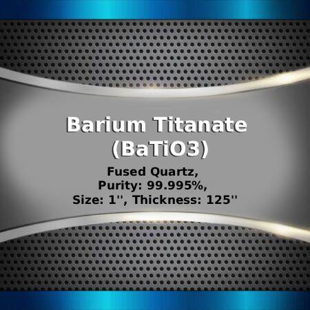
Strontium Titanate (SrTiO3) Sputtering Targets, Purity: 99.9%, Size: 3”, Thickness: 0.125”

$853.00

Applications of Sputtering Targets;

Film deposition is accomplished using sputtering targets. A technique for sputtering thin films is called "deposition made by sputter targets," which entails eroding material from a "target" source onto a "substrate" like a silicon wafer. Etching of the target is done using semiconductor sputtering targets. When selectivity is not an issue and a high degree of etching anisotropy is required, sputter etching is the method of choice. By removing the target material through etching, sputter targets are also utilized for investigation. In secondary ion spectroscopy (SIMS), one example is when the target material is sputtered at a steady pace. Mass spectrometry is used to quantify the concentration and identity of spewed atoms as the target is sputtered.
The target material's composition may be ascertained and even very low concentrations of contaminants can be found with the aid of the sputtering target.

There is also an application area for sputtering targets in space. One type of space weathering that alters the chemical and physical characteristics of airless worlds like the Moon and asteroids is sputtering.

Chromium Oxide (Cr2O3) Sputtering Targets, Purity: 99.8%-99.9%, Size: 4”, Thickness: 0.125”

$854.00

Product 

Chromium Oxide (Cr2O3) Sputtering Targets, Purity: 99.8%-99.9%, Size: 4'', Thickness: 0.125''

CAS No.

1308-38-9

Appearance

Powder

Purity

≥99%,  ≥99.9%,  ≥95%

(Other purities are also available)

APS

 N/A (Size Can be customized), Ask for other available size ranges.

Ingredient

N/A

Molecular Weight

 151.99 g/mol

Melting Point

2,435 °C

Boiling Point

 ~3,000 °C (approximate; may decompose before boiling)

Density

5.21 g/cm³

Product Codes

NCZ-2300K

Lithium Phosphate (Li3PO4) Sputtering Targets, Purity: 99.95%, Size: 3”, Thickness: 0.250”

$855.00

Applications of Sputtering Targets;

Film deposition is accomplished using sputtering targets. A technique for sputtering thin films is called "deposition made by sputter targets," which entails eroding material from a "target" source onto a "substrate" like a silicon wafer. Etching of the target is done using semiconductor sputtering targets. When selectivity is not an issue and a high degree of etching anisotropy is required, sputter etching is the method of choice. By removing the target material through etching, sputter targets are also utilized for investigation. In secondary ion spectroscopy (SIMS), one example is when the target material is sputtered at a steady pace. Mass spectrometry is used to quantify the concentration and identity of spewed atoms as the target is sputtered.

By helping of the sputtering target, the composition of the target material may be evaluated and even extremely tiny amounts of contaminants are recognized.

There is also an application area for sputtering targets in space. One type of space weathering that alters the chemical and physical characteristics of airless worlds like the Moon and asteroids is sputtering.

Tantalum Oxide (Ta2O5) Sputtering Targets, Purity: 99.99%, Size: 3”, Thickness: 0.250”

$855.00

Product 

Tantalum Oxide (Ta2O5) Sputtering Targets, Purity: 99.99%, Size: 3'', Thickness: 0.250''

CAS No.

1314-61-0

Appearance

Powder

Purity

≥99%,  ≥99.9%,  ≥95%

(Other purities are also available)

APS

N/A  (Size Can be customized), Ask for other available size ranges.

Ingredient

N/A

Molecular Weight

 441.89 g/mol

Melting Point

 ~1872 °C

Boiling Point

N/A

Density

~8.2 g/cm³

Product Codes

NCZ-1651K

Vanadium (V) Sputtering Targets, indium, Purity: 99.5%, Size: 3”, Thickness: 0.125”

$856.00

Product 

Vanadium (V) Sputtering Targets, indium, Purity: 99.5%, Size: 3'', Thickness: 0.125''

CAS No.

7440-62-2

Appearance

Powder

Purity

≥99%,  ≥99.9%,  ≥95%

(Other purities are also available)

APS

N/A  (Size Can be customized), Ask for other available size ranges.

Ingredient

N/A

Molecular Weight

50.9415 g/mol

Melting Point

1910 °C

Boiling Point

3407 °C

Density

6.11 g/cm³

Product Codes

NCZ-1543K

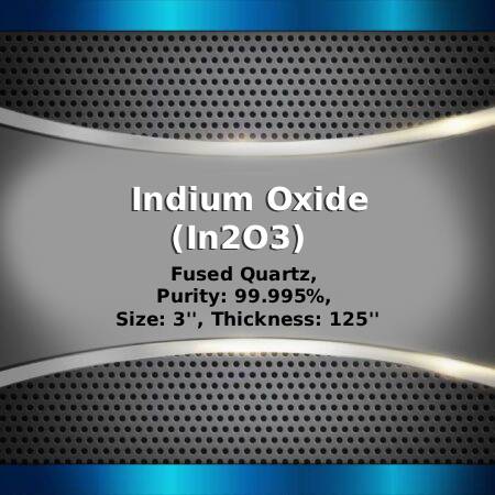
Indium Oxide (In2O3) Sputtering Targets, Purity: 99.99%, Size: 3”, Thickness: 0.125”

$857.00

Product 

Indium Oxide (In2O3) Sputtering Targets, Purity: 99.99%, Size: 3'', Thickness: 0.125''

CAS No.

 1312-43-2

Appearance

Powder

Purity

≥99%,  ≥99.9%,  ≥95%

(Other purities are also available)

APS

< 5 µm (Size Can be customized), Ask for other available size ranges.

Ingredient

N/A

Molecular Weight

 277.64 g/mol

Melting Point

 ~1,910 °C

Boiling Point

 3,000 °C(approx., decomposes)

Density

~7.18 g/cm³ (sintered form)

Product Codes

NCZ-2216K

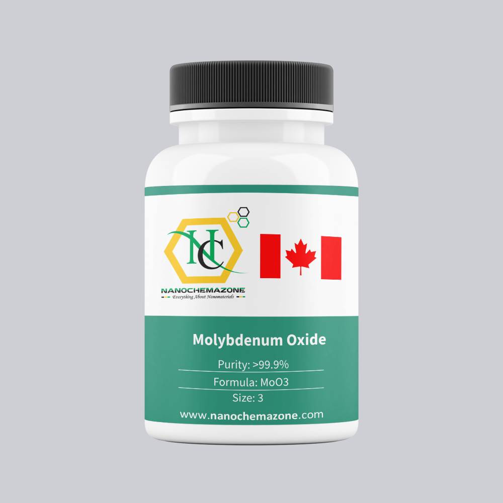
Molybdenum Oxide (MoO3) Sputtering Targets, indium, Purity: 99.9%, Size: 3”, Thickness: 0.125”

$859.00

Applications of Sputtering Targets;

Film deposition is accomplished using sputtering targets. A technique for sputtering thin films is called "deposition made by sputter targets," which entails eroding material from a "target" source onto a "substrate" like a silicon wafer. Etching of the target is done using semiconductor sputtering targets. When selectivity is not an issue and a high degree of etching anisotropy is required, sputter etching is the method of choice. By removing the target material through etching, sputter targets are also utilized for investigation. In secondary ion spectroscopy (SIMS), one example is when the target material is sputtered at a steady pace. Mass spectrometry is used to quantify the concentration and identity of spewed atoms as the target is sputtered.

By helping of the sputtering target, the composition of the target material may be evaluated and even extremely tiny amounts of contaminants are recognized.

There is also an application area for sputtering targets in space. One type of space weathering that alters the chemical and physical characteristics of airless worlds like the Moon and asteroids is sputtering.

Titanium Boride (TiB2) Sputtering Targets, Purity: 99.5%, Size: 4”, Thickness: 0.250”

$860.00

Product 

Titanium Boride (TiB2) Sputtering Targets, Purity: 99.5%, Size: 4'', Thickness: 0.250''

CAS No.

 12045-63-5

Appearance

Powder

Purity

≥99%,  ≥99.9%,  ≥95%

(Other purities are also available)

APS

N/A  (Size Can be customized), Ask for other available size ranges.

Ingredient

N/A

Molecular Weight

69.49 g/mol

Melting Point

 ~3225 °C

Boiling Point

N/A

Density

 4.52 g/cm³

Product Codes

NCZ-1615K

Lithium Niobate (LiNbO3) Sputtering Targets, Purity: 99.9%, Size: 3”, Thickness: 0.250”

$861.00

Product 

Lithium Niobate (LiNbO3) Sputtering Targets, Purity: 99.9%, Size: 3'', Thickness: 0.250''

CAS No.

12031-63-9

Appearance

Powder

Purity

≥99%,  ≥99.9%,  ≥95%

(Other purities are also available)

APS

 N/A (Size Can be customized), Ask for other available size ranges.

Ingredient

N/A

Molecular Weight

 147.85 g/mol

Melting Point

~1,240–1,257 °C

Boiling Point

N/A

Density

~4.30 g/cm³ (ceramic); up to 4.65 g/cm³ (crystal)

Product Codes

NCZ-2038K

Lanthanum Titanate (LaTiO3) Sputtering Targets, Purity: 99.9%, Size: 6”, Thickness: 0.125”

$863.00

Product 

Lanthanum Titanate (LaTiO3) Sputtering Targets, Purity: 99.9%, Size: 6'', Thickness: 0.125''

CAS No.

 12201-04-6

Appearance

Powder

Purity

≥99%,  ≥99.9%,  ≥95%

(Other purities are also available)

APS

<5 µm (Size Can be customized), Ask for other available size ranges.

Ingredient

N/A

Molecular Weight

~234.77 g/mol

Melting Point

~1,770 °C (ceramic decomposes)

Boiling Point

N/A

Density

 ~6.25 g/cm³

Product Codes

NCZ-2084K

Lanthanum Titanate (LaTiO3) Sputtering Targets, Purity: 99.9%, Size: 3”, Thickness: 0.125”

$863.00

Product 

Lanthanum Titanate (LaTiO3) Sputtering Targets, Purity: 99.9%, Size: 3'', Thickness: 0.125''

CAS No.

 12201-04-6

Appearance

Powder

Purity

≥99%,  ≥99.9%,  ≥95%

(Other purities are also available)

APS

<5 µm (Size Can be customized), Ask for other available size ranges.

Ingredient

N/A

Molecular Weight

~234.77 g/mol

Melting Point

~1,770 °C (ceramic decomposes)

Boiling Point

N/A

Density

 ~6.25 g/cm³

Product Codes

NCZ-2090K

Strontium Titanate (SrTiO3) Sputtering Targets, Purity: 99.9%, Size: 4”, Thickness: 0.125”

$864.00

Applications of Sputtering Targets;

Film deposition is accomplished using sputtering targets. A technique for sputtering thin films is called "deposition made by sputter targets," which entails eroding material from a "target" source onto a "substrate" like a silicon wafer. Etching of the target is done using semiconductor sputtering targets. When selectivity is not an issue and a high degree of etching anisotropy is required, sputter etching is the method of choice. By removing the target material through etching, sputter targets are also utilized for investigation. In secondary ion spectroscopy (SIMS), one example is when the target material is sputtered at a steady pace. Mass spectrometry is used to quantify the concentration and identity of spewed atoms as the target is sputtered.

The target material's composition may be ascertained and even very low concentrations of contaminants can be found with the aid of the sputtering target.

There is also an application area for sputtering targets in space. One type of space weathering that alters the chemical and physical characteristics of airless worlds like the Moon and asteroids is sputtering.

Strontium Titanate (SrTiO3) Sputtering Targets, Purity: 99.9%, Size: 7”, Thickness: 0.125”

$864.00

Applications of Sputtering Targets;

Film deposition is accomplished using sputtering targets. A technique for sputtering thin films is called "deposition made by sputter targets," which entails eroding material from a "target" source onto a "substrate" like a silicon wafer. Etching of the target is done using semiconductor sputtering targets. When selectivity is not an issue and a high degree of etching anisotropy is required, sputter etching is the method of choice. By removing the target material through etching, sputter targets are also utilized for investigation. In secondary ion spectroscopy (SIMS), one example is when the target material is sputtered at a steady pace. Mass spectrometry is used to quantify the concentration and identity of spewed atoms as the target is sputtered.

The target material's composition may be ascertained and even very low concentrations of contaminants can be found with the aid of the sputtering target.

There is also an application area for sputtering targets in space. One type of space weathering that alters the chemical and physical characteristics of airless worlds like the Moon and asteroids is sputtering.

Boron Nitride (BN) Sputtering Targets, Purity: 99.5%, Size: 6”, Thickness: 0.250”

$866.00

Product 

Boron Nitride (BN) Sputtering Targets, Purity: 99.5%, Size: 6'', Thickness: 0.250''

CAS No.

 10043-11-5

Appearance

Powder

Purity

≥99%,  ≥99.9%,  ≥95%

(Other purities are also available)

APS

 N/A (Size Can be customized), Ask for other available size ranges.

Ingredient

N/A

Molecular Weight

24.82 g/mol

Melting Point

~2973 °C

Boiling Point

N/A

Density

~2.1 g/cm³

Product Codes

NCZ-2366K

Antimony (Sb) Sputtering Targets, indium, Purity: 99.999%, Size: 3”, Thickness: 0.125”

$866.00

Product 

Antimony (Sb) Sputtering Targets, indium, Purity: 99.999%, Size: 3'', Thickness: 0.125''

CAS No.

 7440-36-0

Appearance

Powder

Purity

≥99%,  ≥99.9%,  ≥95%

(Other purities are also available)

APS

N/A (Size Can be customized), Ask for other available size ranges.

Ingredient

N/A

Molecular Weight

 121.76 g/mol

Melting Point

 630.6 °C

Boiling Point

 1587 °C

Density

 6.69 g/cm³

Product Codes

NCZ-2501K

Aluminum Nitride (AlN) Sputtering Targets, Purity: 99.8%, Size: 3”, Thickness: 0.125”

$866.00

Product 

Aluminum Nitride (AlN) Sputtering Targets, Purity: 99.8%, Size: 3'', Thickness: 0.125''

CAS No.

 24304-00-5

Appearance

Powder

Purity

≥99%,  ≥99.9%,  ≥95%

(Other purities are also available)

APS

N/A (Size Can be customized), Ask for other available size ranges.

Ingredient

N/A

Molecular Weight

40.99 g/mol

Melting Point

 ~2200 °C

Boiling Point

 N/A

Density

 ~3.26 g/cm³

Product Codes

NCZ-2557K

Magnesium Oxide (MgO) Sputtering Targets, indium, Purity: 99.95%, Size:1”, Thickness: 0.125”

$868.00

Applications of Sputtering Targets;

Film deposition is accomplished using sputtering targets. A technique for sputtering thin films is called "deposition made by sputter targets," which entails eroding material from a "target" source onto a "substrate" like a silicon wafer. Etching of the target is done using semiconductor sputtering targets. When selectivity is not an issue and a high degree of etching anisotropy is required, sputter etching is the method of choice. By removing the target material through etching, sputter targets are also utilized for investigation. In secondary ion spectroscopy (SIMS), one example is when the target material is sputtered at a steady pace. Mass spectrometry is used to quantify the concentration and identity of spewed atoms as the target is sputtered.

The target material's composition may be ascertained and even very low concentrations of contaminants can be found with the aid of the sputtering target.

There is also an application area for sputtering targets in space. One type of space weathering that alters the chemical and physical characteristics of airless worlds like the Moon and asteroids is sputtering.

Titanium Nitride (TiN) Sputtering Targets, elastomer, Purity: 99.5%, Size: 2”, Thickness: 0.125”

$869.00

Product 

Titanium Nitride (TiN) Sputtering Targets, elastomer, Purity: 99.5%, Size: 2'', Thickness: 0.125''

CAS No.

25583-20-4

Appearance

Powder

Purity

≥99%,  ≥99.9%,  ≥95%

(Other purities are also available)

APS

N/A  (Size Can be customized), Ask for other available size ranges.

Ingredient

N/A

Molecular Weight

61.88 g/mol

Melting Point

 ~2950 °C

Boiling Point

~4300 °C

Density

5.22 g/cm³

Product Codes

NCZ-1598K

Indium Oxide (In2O3) Sputtering Targets, Purity: 99.99%, Size: 3”, Thickness: 0.250”

$869.00

Product 

Indium Oxide (In2O3) Sputtering Targets, Purity: 99.99%, Size: 3'', Thickness: 0.250''

CAS No.

 1312-43-2

Appearance

Powder

Purity

≥99%,  ≥99.9%,  ≥95%

(Other purities are also available)

APS

< 5 µm (Size Can be customized), Ask for other available size ranges.

Ingredient

N/A

Molecular Weight

 277.64 g/mol

Melting Point

 ~1,910 °C

Boiling Point

 3,000 °C(approx., decomposes)

Density

~7.18 g/cm³ (sintered form)

Product Codes

NCZ-2215K

Cerium Oxide (CeO2) Sputtering Targets, indium, Purity: 99.99%, Size: 2”, Thickness: 0.125”

$869.00

Product 

Cerium Oxide (CeO2) Sputtering Targets, indium, Purity: 99.99%, Size: 2'', Thickness: 0.125''

CAS No.

 1306-38-3

Appearance

Powder

Purity

≥99%,  ≥99.9%,  ≥95%

(Other purities are also available)

APS

 N/A (Size Can be customized), Ask for other available size ranges.

Ingredient

N/A

Molecular Weight

 172.11 g/mol

Melting Point

2,400–2,600 °C

Boiling Point

Sublimes above 3,000 °C

Density

 7.13 g/cm³

Product Codes

NCZ-2317K

Strontium Titanate (SrTiO3) Sputtering Targets, Purity: 99.9%, Size: 1”, Thickness: 0.125”

$870.00

Applications of Sputtering Targets;

Film deposition is accomplished using sputtering targets. A technique for sputtering thin films is called "deposition made by sputter targets," which entails eroding material from a "target" source onto a "substrate" like a silicon wafer. Etching of the target is done using semiconductor sputtering targets. When selectivity is not an issue and a high degree of etching anisotropy is required, sputter etching is the method of choice. By removing the target material through etching, sputter targets are also utilized for investigation. In secondary ion spectroscopy (SIMS), one example is when the target material is sputtered at a steady pace. Mass spectrometry is used to quantify the concentration and identity of spewed atoms as the target is sputtered.

The target material's composition may be ascertained and even very low concentrations of contaminants can be found with the aid of the sputtering target.

There is also an application area for sputtering targets in space. One type of space weathering that alters the chemical and physical characteristics of airless worlds like the Moon and asteroids is sputtering.

Zinc Oxide (ZnO) Sputtering Targets, elastomer, Purity: 99.99%, Size: 2”, Thickness: 0.125”

$872.00

Product 

Zinc Oxide (ZnO) Sputtering Targets, elastomer, Purity: 99.99%, Size: 2'', Thickness: 0.125''

CAS No.

1314-13-2

Appearance

Powder

Purity

≥99%,  ≥99.9%,  ≥95%

(Other purities are also available)

APS

 (ZnO) (Size Can be customized), Ask for other available size ranges.

Ingredient

N/A

Molecular Weight

81.38 g/mol

Melting Point

1975 °C

Boiling Point

N/A

Density

5.61 g/cm³

Product Codes

NCZ-1495K

Zinc Oxide (ZnO) Sputtering Targets, indium, Purity: 99.9% , Size: 2”, Thickness: 0.125”

$872.00

Product 

Zinc Oxide (ZnO) Sputtering Targets, indium, Purity: 99.9% , Size: 2'', Thickness: 0.125''

CAS No.

1314-13-2

Appearance

Powder

Purity

≥99%,  ≥99.9%,  ≥95%

(Other purities are also available)

APS

 (ZnO) (Size Can be customized), Ask for other available size ranges.

Ingredient

N/A

Molecular Weight

81.38 g/mol

Melting Point

1975 °C

Boiling Point

N/A

Density

5.61 g/cm³

Product Codes

NCZ-1498K

Zinc Sulfide (ZnS) Sputtering Targets, Purity: 99.99%, Size: 4”, Thickness: 0.250”

$873.00

Applications of Sputtering Targets;

Film deposition is accomplished using sputtering targets. A technique for sputtering thin films is called "deposition made by sputter targets," which entails eroding material from a "target" source onto a "substrate" like a silicon wafer. Etching of the target is done using semiconductor sputtering targets. When selectivity is not an issue and a high degree of etching anisotropy is required, sputter etching is the method of choice. By removing the target material through etching, sputter targets are also utilized for investigation. In secondary ion spectroscopy (SIMS), one example is when the target material is sputtered at a steady pace. Mass spectrometry is used to quantify the concentration and identity of spewed atoms as the target is sputtered.

The target material's composition may be ascertained and even very low concentrations of contaminants can be found with the aid of the sputtering target.

There is also an application area for sputtering targets in space. One type of space weathering that alters the chemical and physical characteristics of airless worlds like the Moon and asteroids is sputtering.

Titanium Carbide (TiC) Sputtering Targets, Purity: 99.5%, Size: 4”, Thickness: 0.125”

$874.00

Product 

Titanium Carbide (TiC) Sputtering Targets, Purity: 99.5%, Size: 4'', Thickness: 0.125''

CAS No.

 12070-08-5

Appearance

Powder

Purity

≥99%,  ≥99.9%,  ≥95%

(Other purities are also available)

APS

N/A  (Size Can be customized), Ask for other available size ranges.

Ingredient

N/A

Molecular Weight

59.89 g/mol

Melting Point

 ~3160 °C

Boiling Point

N/A

Density

4.93 g/cm³

Product Codes

NCZ-1608K

Titanium Carbide (TiC) Sputtering Targets, Purity: 99.5%, Size: 4”, Thickness: 0.125”

$874.00

Product 

Titanium Carbide (TiC) Sputtering Targets, Purity: 99.5%, Size: 4'', Thickness: 0.125''

CAS No.

 12070-08-5

Appearance

Powder

Purity

≥99%,  ≥99.9%,  ≥95%

(Other purities are also available)

APS

N/A  (Size Can be customized), Ask for other available size ranges.

Ingredient

N/A

Molecular Weight

59.89 g/mol

Melting Point

 ~3160 °C

Boiling Point

N/A

Density

4.93 g/cm³

Product Codes

NCZ-1608K

Lanthanum Titanate (LaTiO3) Sputtering Targets, Purity: 99.9%, Size: 4”, Thickness: 0.250”

$875.00

Applications of Sputtering Targets;

  • Sputtering targets is used for film deposition. The deposition made by sputter targets is a method of depositing thin films by sputtering that involves eroding material from a "target" source onto a "substrate" such as  a silicon wafer.
  • Semiconductor sputtering targets is used to etch the target. Sputter etching is chosen in cases where a high degree of etching anisotropy is needed and selectivity is not a concern.
  • Sputter targets is also used for analysis by etching away the target material.
One of the example occurs in secondary ion spectroscopy (SIMS), where the target sample is sputtered at a constant rate. As the target is sputtered, the concentration and identity of sputtered atoms are measured using mass spectrometry. By helping of the sputtering target, the composition of the target material can be determined and even extremely low concentrations of impurities are detected. Sputtering target has also application area in space. Sputtering is one of the forms of space weathering, a process that changes the physical and chemical properties of airless bodies, such as asteroids and the Moon.

Titanium Boride (TiB2) Sputtering Targets, Purity: 99.5%, Size: 4”, Thickness: 0.125”

$876.00

Product 

Titanium Boride (TiB2) Sputtering Targets, Purity: 99.5%, Size: 4'', Thickness: 0.125''

CAS No.

 12045-63-5

Appearance

Powder

Purity

≥99%,  ≥99.9%,  ≥95%

(Other purities are also available)

APS

N/A  (Size Can be customized), Ask for other available size ranges.

Ingredient

N/A

Molecular Weight

69.49 g/mol

Melting Point

 ~3225 °C

Boiling Point

N/A

Density

 4.52 g/cm³

Product Codes

NCZ-1616K

Indium Oxide (In2O3) Sputtering Targets, Purity: 99.99%, Size: 4”, Thickness: 0.125”

$876.00

Product 

Indium Oxide (In2O3) Sputtering Targets, Purity: 99.99%, Size: 4'', Thickness: 0.125''

CAS No.

 1312-43-2

Appearance

Powder

Purity

≥99%,  ≥99.9%,  ≥95%

(Other purities are also available)

APS

< 5 µm (Size Can be customized), Ask for other available size ranges.

Ingredient

N/A

Molecular Weight

 277.64 g/mol

Melting Point

 ~1,910 °C

Boiling Point

 3,000 °C(approx., decomposes)

Density

~7.18 g/cm³ (sintered form)

Product Codes

NCZ-2214K