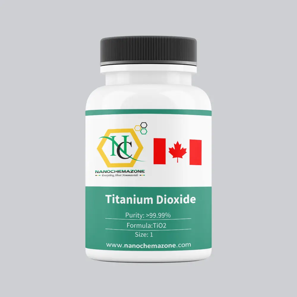
Strontium Titanate (SrTiO3) Sputtering Targets, Purity: 99.9%, Size: 4”, Thickness: 0.250”

$780.00

Product 

Strontium Titanate (SrTiO3) Sputtering Targets, Purity: 99.9%, Size: 4'', Thickness: 0.250''

CAS No.

12060-08-1

Appearance

Powder

Purity

≥99%,  ≥99.9%,  ≥95%

(Other purities are also available)

APS

N/A  (Size Can be customized), Ask for other available size ranges.

Ingredient

N/A

Molecular Weight

183.49 g/mol

Melting Point

 ~2080 °C

Boiling Point

N/A

Density

~5.12 g/cm³

Product Codes

NCZ-1677K

Silicon Nitride (Si3N4) Sputtering Targets, Purity: 99.5%, Size: 3”, Thickness: 0.125”, Dark Gray to Black

$780.00

Product 

Silicon Nitride (Si3N4) Sputtering Targets, Purity: 99.5%, Size: 3'', Thickness: 0.125'', Dark Gray to Black

CAS No.

 12033-89-5

Appearance

Powder

Purity

≥99%,  ≥99.9%,  ≥95%

(Other purities are also available)

APS

N/A  (Size Can be customized), Ask for other available size ranges.

Ingredient

N/A

Molecular Weight

 140.28 g/mol

Melting Point

 ~1900 °C

Boiling Point

N/A

Density

~3.2 g/cm³

Product Codes

NCZ-1697K

Iron Oxide (Fe3O4) Sputtering Targets, Purity: 99.9%, Size: 3”, Thickness: 0.250”

$780.00

Product 

Iron Oxide (Fe3O4) Sputtering Targets, Purity: 99.9%, Size: 3'', Thickness: 0.250''

CAS No.

1317‑61‑9

Appearance

Powder

Purity

≥99%,  ≥99.9%,  ≥95%

(Other purities are also available)

APS

 N/A (Size Can be customized), Ask for other available size ranges.

Ingredient

N/A

Molecular Weight

 231.6 g/mol

Melting Point

~1,597 °C

Boiling Point

 ~2,623 °C (material may decompose before boiling)

Density

 ~5.17 g/cm³ (sintered target)

Product Codes

NCZ-2172K

Molybdenum Disulfide (MoS2) Sputtering Targets, Purity: 99.9%, Size: 4”, Thickness: 0.125”

$781.00

Applications of Sputtering Targets;

Film deposition is accomplished using sputtering targets. A technique for sputtering thin films is called "deposition made by sputter targets," which entails eroding material from a "target" source onto a "substrate" like a silicon wafer. Etching of the target is done using semiconductor sputtering targets. When selectivity is not an issue and a high degree of etching anisotropy is required, sputter etching is the method of choice. By removing the target material through etching, sputter targets are also utilized for investigation. In secondary ion spectroscopy (SIMS), one example is when the target material is sputtered at a steady pace. Mass spectrometry is used to quantify the concentration and identity of spewed atoms as the target is sputtered.

By helping of the sputtering target, the composition of the target material may be evaluated and even extremely tiny amounts of contaminants are recognized.

There is also an application area for sputtering targets in space. One type of space weathering that alters the chemical and physical characteristics of airless worlds like the Moon and asteroids is sputtering.

Zinc Oxide (ZnO) Sputtering Targets, indium, Purity: 99.99%, Size: 2”, Thickness: 0.125”

$781.00

Applications of Sputtering Targets;

Film deposition is accomplished using sputtering targets. A technique for sputtering thin films is called "deposition made by sputter targets," which entails eroding material from a "target" source onto a "substrate" like a silicon wafer. Etching of the target is done using semiconductor sputtering targets. When selectivity is not an issue and a high degree of etching anisotropy is required, sputter etching is the method of choice. By removing the target material through etching, sputter targets are also utilized for investigation. In secondary ion spectroscopy (SIMS), one example is when the target material is sputtered at a steady pace. Mass spectrometry is used to quantify the concentration and identity of spewed atoms as the target is sputtered.

The target material's composition may be ascertained and even very low concentrations of contaminants can be found with the aid of the sputtering target.

There is also an application area for sputtering targets in space. One type of space weathering that alters the chemical and physical characteristics of airless worlds like the Moon and asteroids is sputtering.

Lanthanum Manganate (LaMnO3) Sputtering Targets, Purity: 99.9%, Size: 1”, Thickness: 0.250”

$781.00

Product 

Lanthanum Manganate (LaMnO3) Sputtering Targets, Purity: 99.9%, Size: 1'', Thickness: 0.250''

CAS No.

13538-87-7

Appearance

Powder

Purity

≥99%,  ≥99.9%,  ≥95%

(Other purities are also available)

APS

 ~1–5 µm (Size Can be customized), Ask for other available size ranges.

Ingredient

N/A

Molecular Weight

240.83 g/mol

Melting Point

N/A

Boiling Point

N/A

Density

~6.3 – 6.8 g/cm³

Product Codes

NCZ-2141K

Iron Oxide (Fe3O4) Sputtering Targets, indium, Purity: 99.9%, Size: 2”, Thickness: 0.125”

$782.00

Applications of Sputtering Targets;

Film deposition is accomplished using sputtering targets. A technique for sputtering thin films is called "deposition made by sputter targets," which entails eroding material from a "target" source onto a "substrate" like a silicon wafer. Etching of the target is done using semiconductor sputtering targets. When selectivity is not an issue and a high degree of etching anisotropy is required, sputter etching is the method of choice. By removing the target material through etching, sputter targets are also utilized for investigation. In secondary ion spectroscopy (SIMS), one example is when the target material is sputtered at a steady pace. Mass spectrometry is used to quantify the concentration and identity of spewed atoms as the target is sputtered.

The target material's composition may be ascertained and even very low concentrations of contaminants can be found with the aid of the sputtering target.

There is also an application area for sputtering targets in space. One type of space weathering that alters the chemical and physical characteristics of airless worlds like the Moon and asteroids is sputtering.

Praseodymium Calcium Manganate (Pr0.7Ca0.3MnO3) Sputtering Targets, Purity: 99.9%, Size: 1”, Thickness: 0.125”

$782.00

Product 

Praseodymium Calcium Manganate (Pr0.7Ca0.3MnO3) Sputtering Targets, Purity: 99.9%, Size: 1'', Thickness: 0.125''

CAS No.

N/A

Appearance

Powder

Purity

≥99%,  ≥99.9%,  ≥95%

(Other purities are also available)

APS

1–5 μm (Size Can be customized), Ask for other available size ranges.

Ingredient

N/A

Molecular Weight

237.66 g/mol

Melting Point

N/A

Boiling Point

N/A

Density

~6.4–6.8 g/cm³

Product Codes

NCZ-1783K

Titanium Nitride (TiN) Sputtering Targets, indium, Purity: 99.5%, Size: 2”, Thickness: 0.125”

$783.00

Applications of Sputtering Targets;

Film deposition is accomplished using sputtering targets. A technique for sputtering thin films is called "deposition made by sputter targets," which entails eroding material from a "target" source onto a "substrate" like a silicon wafer. Etching of the target is done using semiconductor sputtering targets. When selectivity is not an issue and a high degree of etching anisotropy is required, sputter etching is the method of choice. By removing the target material through etching, sputter targets are also utilized for investigation. In secondary ion spectroscopy (SIMS), one example is when the target material is sputtered at a steady pace. Mass spectrometry is used to quantify the concentration and identity of spewed atoms as the target is sputtered.

The target material's composition may be ascertained and even very low concentrations of contaminants can be found with the aid of the sputtering target.

There is also an application area for sputtering targets in space. One type of space weathering that alters the chemical and physical characteristics of airless worlds like the Moon and asteroids is sputtering.

Lanthanum Titanate (LaTiO3) Sputtering Targets, Purity: 99.9%, Size: 2”, Thickness: 0.125”

$783.00

Product 

Lanthanum Titanate (LaTiO3) Sputtering Targets, Purity: 99.9%, Size: 2'', Thickness: 0.125''

CAS No.

12031‑47‑9 (specific to size) or 12201‑04‑6 (general LaTiO₃)

Appearance

Powder

Purity

≥99%,  ≥99.9%,  ≥95%

(Other purities are also available)

APS

<5 µm (Size Can be customized), Ask for other available size ranges.

Ingredient

N/A

Molecular Weight

 234.77 g/mol (exact ~234.839 g/mol)

Melting Point

 Approx. 2,200 °C

Boiling Point

N/A

Density

N/A

Product Codes

NCZ-2092K

Bismuth Oxide (Bi2O3) Sputtering Targets, Purity: 99.9%, Size: 3”, Thickness: 0.250”

$783.00

Product 

Bismuth Oxide (Bi2O3) Sputtering Targets, Purity: 99.9%, Size: 3'', Thickness: 0.250''

CAS No.

 1304-76-3

Appearance

Powder

Purity

≥99%,  ≥99.9%,  ≥95%

(Other purities are also available)

APS

 N/A (Size Can be customized), Ask for other available size ranges.

Ingredient

N/A

Molecular Weight

465.96 g/mol

Melting Point

 ~817 °C

Boiling Point

N/A

Density

 ~8.9 g/cm³

Product Codes

NCZ-2407K

Bismuth Oxide (Bi2O3) Sputtering Targets, Purity: 99.9%, Size: 3”, Thickness: 0.125”

$783.00

Product 

Bismuth Oxide (Bi2O3) Sputtering Targets, Purity: 99.9%, Size: 3'', Thickness: 0.125''

CAS No.

 1304-76-3

Appearance

Powder

Purity

≥99%,  ≥99.9%,  ≥95%

(Other purities are also available)

APS

 N/A (Size Can be customized), Ask for other available size ranges.

Ingredient

N/A

Molecular Weight

465.96 g/mol

Melting Point

 ~817 °C

Boiling Point

N/A

Density

 ~8.9 g/cm³

Product Codes

NCZ-2408K

Silicon Carbide (SiC) Sputtering Targets, indium, Purity: 99.5%, Size: 1”, Thickness: 0.125”

$785.00

Product 

Silicon Carbide (SiC) Sputtering Targets, indium, Purity: 99.5%, Size: 1'', Thickness: 0.125''

CAS No.

 409-21-2

Appearance

Powder

Purity

≥99%,  ≥99.9%,  ≥95%

(Other purities are also available)

APS

N/A  (Size Can be customized), Ask for other available size ranges.

Ingredient

N/A

Molecular Weight

 40.10 g/mol

Melting Point

~2,700 °C

Boiling Point

N/A

Density

~3.21 g/cm³

Product Codes

NCZ-1723K

Magnesium Oxide (MgO) Sputtering Targets, Purity: 99.95%, Size: 6”, Thickness: 0.125”

$786.00

Product 

Magnesium Oxide (MgO) Sputtering Targets, Purity: 99.95%, Size: 6'', Thickness: 0.125''

CAS No.

1309-48-4

Appearance

Powder

Purity

≥99%,  ≥99.9%,  ≥95%

(Other purities are also available)

APS

 N/A (Size Can be customized), Ask for other available size ranges.

Ingredient

N/A

Molecular Weight

40.30 g/mol

Melting Point

 ~2852 °C

Boiling Point

~3600 °C

Density

 ~3.58 g/cm³

Product Codes

NCZ-1966K

Lithium Cobalt Oxide (LiCoO2) Sputtering Targets, indium, Purity: 99.9%, Size: 2”, Thickness: 0.125”

$787.00

Applications of Sputtering Targets;

Film deposition is accomplished using sputtering targets. A technique for sputtering thin films is called "deposition made by sputter targets," which entails eroding material from a "target" source onto a "substrate" like a silicon wafer. Etching of the target is done using semiconductor sputtering targets. When selectivity is not an issue and a high degree of etching anisotropy is required, sputter etching is the method of choice. By removing the target material through etching, sputter targets are also utilized for investigation. In secondary ion spectroscopy (SIMS), one example is when the target material is sputtered at a steady pace. Mass spectrometry is used to quantify the concentration and identity of spewed atoms as the target is sputtered.

The target material's composition may be ascertained and even very low concentrations of contaminants can be found with the aid of the sputtering target.

There is also an application area for sputtering targets in space. One type of space weathering that alters the chemical and physical characteristics of airless worlds like the Moon and asteroids is sputtering.

Formula LiCoO2 represents the chemical compound lithium cobalt oxide. A crystalline solid that is dark blue or bluish-gray in color, lithium cobalt oxide is frequently utilized in the positive electrodes of lithium-ion batteries.

Lithium Cobalt Oxide (LiCoO2) Sputtering Targets, indium, Purity: 99.9%, Size: 2”, Thickness: 0.125”

$787.00

Applications of Sputtering Targets;

Film deposition is accomplished using sputtering targets. A technique for sputtering thin films is called "deposition made by sputter targets," which entails eroding material from a "target" source onto a "substrate" like a silicon wafer. Etching of the target is done using semiconductor sputtering targets. When selectivity is not an issue and a high degree of etching anisotropy is required, sputter etching is the method of choice. By removing the target material through etching, sputter targets are also utilized for investigation. In secondary ion spectroscopy (SIMS), one example is when the target material is sputtered at a steady pace. Mass spectrometry is used to quantify the concentration and identity of spewed atoms as the target is sputtered.

The target material's composition may be ascertained and even very low concentrations of contaminants can be found with the aid of the sputtering target.

There is also an application area for sputtering targets in space. One type of space weathering that alters the chemical and physical characteristics of airless worlds like the Moon and asteroids is sputtering.

Formula LiCoO2 represents the chemical compound lithium cobalt oxide. A crystalline solid that is dark blue or bluish-gray in color, lithium cobalt oxide is frequently utilized in the positive electrodes of lithium-ion batteries.

Yttrium Ferrite (Y3Fe5O12) Sputtering Targets, Purity: 99.9%, Size: 1”, Thickness: 0.250”

$788.00

Applications of Sputtering Targets;

  • Sputtering targets is used for film deposition. The deposition made by sputter targets is a method of depositing thin films by sputtering that involves eroding material from a "target" source onto a "substrate" such as  a silicon wafer.
  • Semiconductor sputtering targets is used to etch the target. Sputter etching is chosen in cases where a high degree of etching anisotropy is needed and selectivity is not a concern.
  • Sputter targets is also used for analysis by etching away the target material.
One of the example occurs in secondary ion spectroscopy (SIMS), where the target sample is sputtered at a constant rate. As the target is sputtered, the concentration and identity of sputtered atoms are measured using mass spectrometry. By helping of the sputtering target, the composition of the target material can be determined and even extremely low concentrations of impurities are detected. Sputtering target has also application area in space. Sputtering is one of the forms of space weathering, a process that changes the physical and chemical properties of airless bodies, such as asteroids and the Moon.

Aluminum Nitride (AlN) Sputtering Targets, Purity: 99.8%, Size: 2”, Thickness: 0.250”

$788.00

Applications of Sputtering Targets;

  • Sputtering targets is used for film deposition. The deposition made by sputter targets is a method of depositing thin films by sputtering that involves eroding material from a "target" source onto a "substrate" such as  a silicon wafer.
  • Semiconductor sputtering targets is used to etch the target. Sputter etching is chosen in cases where a high degree of etching anisotropy is needed and selectivity is not a concern.
  • Sputter targets is also used for analysis by etching away the target material.
One of the example occurs in secondary ion spectroscopy (SIMS), where the target sample is sputtered at a constant rate. As the target is sputtered, the concentration and identity of sputtered atoms are measured using mass spectrometry. By helping of the sputtering target, the composition of the target material can be determined and even extremely low concentrations of impurities are detected. Sputtering target has also application area in space. Sputtering is one of the forms of space weathering, a process that changes the physical and chemical properties of airless bodies, such as asteroids and the Moon. Aluminum nitride is a chemical compound with the formula of AlN.Aluminum nitride has excellent combination of physical, chemical, and mechanical properties. High-quality films of aluminum nitride have been used in various devices and sensors including the optical and optoelectronic devices. As far as the optical and optoelectronic applications are concerned, wide band gap (~6.2 eV) along with high-refractive index (~2.0) and low-absorption coefficient (<10−3) makes AlN a very attractive material for these applications. In addition to this, thermal and chemical stability of AlN films make it suitable for applications in difficult environment. Today, AlN films/coatings have been grown by several methods which include pulsed laser deposition, reactive molecular beam epitaxy, vacuum arc/cathodic arc deposition, DC/RF reactive sputtering, ion beam sputtering, metal-organic chemical vapor deposition (MOCVD), and miscellaneous other techniques. Due to simplicity, reproducibility, ease of scaling up, and lower cost, magnetron sputtering is one of the common methods for growing AlN films for various applications. Properties of AlN films depend upon the crystal structure, crystal orientation, microstructure, and chemical composition, which in turn depend upon the deposition conditions such as sputtering power, pulse frequency, duty cycle, growth temperature, nitrogen/argon flow ratio, and sputtering gas pressure. AlN sputtering targets give good result with the method of reactive DC magnetron sputtering system.

Aluminum Nitride (AlN) Sputtering Targets, Purity: 99.8%, Size: 2”, Thickness: 0.250”

$788.00

Applications of Sputtering Targets;

Film deposition is accomplished using sputtering targets. A technique for sputtering thin films is called "deposition made by sputter targets," which entails eroding material from a "target" source onto a "substrate" like a silicon wafer. Etching of the target is done using semiconductor sputtering targets. When selectivity is not an issue and a high degree of etching anisotropy is required, sputter etching is the method of choice. By removing the target material through etching, sputter targets are also utilized for investigation. In secondary ion spectroscopy (SIMS), one example is when the target material is sputtered at a steady pace. Mass spectrometry is used to quantify the concentration and identity of spewed atoms as the target is sputtered. With the sputtering target's assistance, the

It is possible to identify the target material and even detect incredibly tiny impurity amounts.

There is also an application area for sputtering targets in space. One type of space weathering that alters the chemical and physical characteristics of airless worlds like the Moon and asteroids is sputtering.

The chemical compound aluminum nitride has the formula AlN. The combination of mechanical, chemical, and physical properties of aluminum nitride is exceptional. Superior aluminum nitride films have found application in a wide range of sensors and devices, including optoelectronic and optical ones. Regarding optical and optoelectronic applications, AlN is a very desirable material due to its broad band gap (~6.2 eV), high refractive index (~2.0), and low absorption coefficient (<10−3).

Iron Oxide (Fe3O4) Sputtering Targets, Purity: 99.9%, Size: 4”, Thickness: 0.250”

$788.00

Applications of Sputtering Targets;

Film deposition is accomplished using sputtering targets. A technique for sputtering thin films is called "deposition made by sputter targets," which entails eroding material from a "target" source onto a "substrate" like a silicon wafer. Etching of the target is done using semiconductor sputtering targets. When selectivity is not an issue and a high degree of etching anisotropy is required, sputter etching is the method of choice. By removing the target material through etching, sputter targets are also utilized for investigation. In secondary ion spectroscopy (SIMS), one example is when the target material is sputtered at a steady pace. Mass spectrometry is used to quantify the concentration and identity of spewed atoms as the target is sputtered.

The target material's composition may be ascertained and even very low concentrations of contaminants can be found with the aid of the sputtering target.

There is also an application area for sputtering targets in space. One type of space weathering that alters the chemical and physical characteristics of airless worlds like the Moon and asteroids is sputtering.

Yttrium Ferrite (Y3Fe5O12) Sputtering Targets, indium, Purity: 99.9%, Size: 2”, Thickness: 0.125”

$790.00

Product 

Yttrium Ferrite (Y3Fe5O12) Sputtering Targets, indium, Purity: 99.9%, Size: 2'', Thickness: 0.125''

CAS No.

12068-40-5

Appearance

Powder

Purity

≥99%,  ≥99.9%,  ≥95%

(Other purities are also available)

APS

 N/A (Size Can be customized), Ask for other available size ranges.

Ingredient

N/A

Molecular Weight

706.32 g/mol

Melting Point

~1,790 °C

Boiling Point

N/A

Density

~5.17 – 5.36

Product Codes

NCZ-1511K

Lanthanum Aluminate (LaAlO3) Sputtering Targets, indium, Purity: 99.9%, Size: 1”, Thickness: 0.125”

$791.00

Product 

Lanthanum Aluminate (LaAlO3) Sputtering Targets, indium, Purity: 99.9%, Size: 1'', Thickness: 0.125''

CAS No.

 12003‑65‑5

Appearance

Powder

Purity

≥99%,  ≥99.9%,  ≥95%

(Other purities are also available)

APS

 N/A (Size Can be customized), Ask for other available size ranges.

Ingredient

N/A

Molecular Weight

~213.89 g/mol

Melting Point

~2,080 °C

Boiling Point

N/A

Density

 ~6.52 g/cm³

Product Codes

NCZ-2160K

Lanthanum Strontium Manganate (La0.7Sr0.3MnO3) Sputtering Targets, Purity: 99.9%, Size: 2”, Thickness: 0.250”

$792.00
but allow experts a large degree of control over the growth and microstructure of the area.

Applications of Sputtering Targets;

  • Sputtering targets is used for film deposition. The deposition made by sputter targets is a method of depositing thin films by sputtering that involves eroding material from a "target" source onto a "substrate" such as  a silicon wafer.
  • Semiconductor sputtering targets is used to etch the target. Sputter etching is chosen in cases where a high degree of etching anisotropy is needed and selectivity is not a concern.
  • Sputter targets is also used for analysis by etching away the target material.
One of the example occurs  in secondary ion spectroscopy (SIMS), where the target sample is sputtered at a constant rate. As the target is sputtered, the concentration and identity of sputtered atoms are measured using mass spectrometry. By helping of the sputtering target, the composition of the target material can be determined and even extremely low concentrations of impurities are detected. Sputtering target has also application area in space. Sputtering is one of the forms of space weathering, a process that changes the physical and chemical properties of airless bodies, such as asteroids and the Moon.

Lithium Phosphate (Li3PO4) Sputtering Targets, elastomer, Purity: 99.95%, Size: 1”, Thickness: 0.125”

$792.00

Applications of Sputtering Targets;

Film deposition is accomplished using sputtering targets. A technique for sputtering thin films is called "deposition made by sputter targets," which entails eroding material from a "target" source onto a "substrate" like a silicon wafer. Etching of the target is done using semiconductor sputtering targets. When selectivity is not an issue and a high degree of etching anisotropy is required, sputter etching is the method of choice. By removing the target material through etching, sputter targets are also utilized for investigation. In secondary ion spectroscopy (SIMS), one example is when the target material is sputtered at a steady pace. Mass spectrometry is used to quantify the concentration and identity of spewed atoms as the target is sputtered.

By helping of the sputtering target, the composition of the target material may be evaluated and even extremely tiny amounts of contaminants are recognized.

There is also an application area for sputtering targets in space. One type of space weathering that alters the chemical and physical characteristics of airless worlds like the Moon and asteroids is sputtering.

Magnesium Fluoride (MgF2) Sputtering Targets, Purity: 99.9%, Size: 6”, Thickness: 0.250”

$792.00

Applications of Sputtering Targets;

Film deposition is accomplished using sputtering targets. A technique for sputtering thin films is called "deposition made by sputter targets," which entails eroding material from a "target" source onto a "substrate" like a silicon wafer. Etching of the target is done using semiconductor sputtering targets. When selectivity is not an issue and a high degree of etching anisotropy is required, sputter etching is the method of choice. By removing the target material through etching, sputter targets are also utilized for investigation. In secondary ion spectroscopy (SIMS), one example is when the target material is sputtered at a steady pace. Mass spectrometry is used to quantify the concentration and identity of spewed atoms as the target is sputtered.

By helping of the sputtering target, the composition of the target material may be evaluated and even extremely tiny amounts of contaminants are recognized.

There is also an application area for sputtering targets in space. One type of space weathering that alters the chemical and physical characteristics of airless worlds like the Moon and asteroids is sputtering.

Lithium Cobalt Oxide (LiCoO2) Sputtering Targets, Purity: 99.9%, Size: 3”, Thickness: 0.250”

$794.00

Applications of Sputtering Targets;

Film deposition is accomplished using sputtering targets. A technique for sputtering thin films is called "deposition made by sputter targets," which entails eroding material from a "target" source onto a "substrate" like a silicon wafer. Etching of the target is done using semiconductor sputtering targets. When selectivity is not an issue and a high degree of etching anisotropy is required, sputter etching is the method of choice. By removing the target material through etching, sputter targets are also utilized for investigation. In secondary ion spectroscopy (SIMS), one example is when the target material is sputtered at a steady pace. Mass spectrometry is used to quantify the concentration and identity of spewed atoms as the target is sputtered.

Even very low quantities of contaminants can be detected with the aid of the sputtering target, allowing for the determination of the target material's composition.

Applications for sputtering targets are also found in space. One type of space weathering is sputtering, which modifies the chemical and physical characteristics of airless worlds like the Moon and asteroids.

LiCoO2 is the formula for the chemical compound lithium cobalt oxide. The positive electrodes of lithium-ion batteries frequently include lithium cobalt oxide, a crystalline solid with a dark blue or bluish-gray color.

Lithium Cobalt Oxide (LiCoO2) Sputtering Targets, Purity: 99.9%, Size: 3”, Thickness: 0.250”

$794.00

Applications of Sputtering Targets;

Film deposition is accomplished using sputtering targets. A technique for sputtering thin films is called "deposition made by sputter targets," which entails eroding material from a "target" source onto a "substrate" like a silicon wafer. Etching of the target is done using semiconductor sputtering targets. When selectivity is not an issue and a high degree of etching anisotropy is required, sputter etching is the method of choice. By removing the target material through etching, sputter targets are also utilized for investigation. In secondary ion spectroscopy (SIMS), one example is when the target material is sputtered at a steady pace. Mass spectrometry is used to quantify the concentration and identity of spewed atoms as the target is sputtered. With the sputtering target's assistance,

There is also an application area for sputtering targets in space. One type of space weathering that alters the chemical and physical characteristics of airless worlds like the Moon and asteroids is sputtering.

Formula LiCoO2 represents the chemical compound lithium cobalt oxide. A crystalline solid that is dark blue or bluish-gray in color, lithium cobalt oxide is frequently utilized in the positive electrodes of lithium-ion batteries.

Let's now examine the potential use of lithium cobalt oxide sputtering targets in batteries. Very small battery sizes are of great importance since portable microelectronic devices and sensors are getting smaller and smaller all the time.

Titanium Boride (TiB2) Sputtering Targets, indium, Purity: 99.5%, Size: 2”, Thickness: 0.125”

$795.00

Product 

Titanium Boride (TiB2) Sputtering Targets, indium, Purity: 99.5%, Size: 2'', Thickness: 0.125''

CAS No.

 12045-63-5

Appearance

Powder

Purity

≥99%,  ≥99.9%,  ≥95%

(Other purities are also available)

APS

N/A  (Size Can be customized), Ask for other available size ranges.

Ingredient

N/A

Molecular Weight

69.49 g/mol

Melting Point

 ~3225 °C

Boiling Point

N/A

Density

 4.52 g/cm³

Product Codes

NCZ-1614K

Tantalum (Ta) Sputtering Targets, Purity: 99.95%, Size: 3”, Thickness: 0.250”

$797.00

Product 

Tantalum (Ta) Sputtering Targets, Purity: 99.95%, Size: 3'', Thickness: 0.250''

CAS No.

 7440-25-7

Appearance

Powder

Purity

≥99%,  ≥99.9%,  ≥95%

(Other purities are also available)

APS

N/A  (Size Can be customized), Ask for other available size ranges.

Ingredient

N/A

Molecular Weight

 180.95 g/mol

Melting Point

3017 °C

Boiling Point

 5458 °C

Density

16.65 g/cm³

Product Codes

NCZ-1662K

Indium (In) Sputtering Targets, Purity: 99.999%, Size: 4”, Thickness: 0.250”

$799.00

Product 

Indium (In) Sputtering Targets, Purity: 99.999%, Size: 4'', Thickness: 0.250''

CAS No.

 7440-74-6

Appearance

Powder

Purity

≥99%,  ≥99.9%,  ≥95%

(Other purities are also available)

APS

 N/A (Size Can be customized), Ask for other available size ranges.

Ingredient

N/A

Molecular Weight

114.82 g/mol

Melting Point

 156.6 °C

Boiling Point

 2,072 °C

Density

 7.31 g/cm³

Product Codes

NCZ-2220K

Strontium Titanate (SrTiO3) Sputtering Targets, Purity: 99.9%, Size: 5”, Thickness: 0.250”

$801.00

Product 

Strontium Titanate (SrTiO3) Sputtering Targets, Purity: 99.9%, Size: 5'', Thickness: 0.250''

CAS No.

12060-08-1

Appearance

Powder

Purity

≥99%,  ≥99.9%,  ≥95%

(Other purities are also available)

APS

N/A  (Size Can be customized), Ask for other available size ranges.

Ingredient

N/A

Molecular Weight

183.49 g/mol

Melting Point

 ~2080 °C

Boiling Point

N/A

Density

~5.12 g/cm³

Product Codes

NCZ-1675K

Bismuth Telluride (Bi2Te3) Sputtering Targets, Purity: 99.999%, Size: 2”, Thickness: 0.125”

$802.00

Applications of Sputtering Targets;

Film deposition is accomplished using sputtering targets. A technique for sputtering thin films is called "deposition made by sputter targets," which entails eroding material from a "target" source onto a "substrate" like a silicon wafer. Etching of the target is done using semiconductor sputtering targets. When selectivity is not an issue and a high degree of etching anisotropy is required, sputter etching is the method of choice. By removing the target material through etching, sputter targets are also utilized for investigation. In secondary ion spectroscopy (SIMS), one example is when the target material is sputtered at a steady pace. Mass spectrometry is used to quantify the concentration and identity of spewed atoms as the target is sputtered.

The target material's composition may be ascertained and even very low concentrations of contaminants can be found with the aid of the sputtering target.

There is also an application area for sputtering targets in space. One type of space weathering that alters the chemical and physical characteristics of airless worlds like the Moon and asteroids is sputtering.

Bi2Te3, or bismuth telluride, is a gray powder that is a combination of bismuth and tellurium. It is a semiconductor that becomes an effective thermoelectric material for refrigeration or portable power generation when alloyed with antimony or selenium. Since Bi2Te3 is a topological insulator, its physical characteristics depend on its thickness.
Bismuth Oxide (Bi2O3) Sputtering Targets, indium, Purity: 99.9%, Size: 2”, Thickness: 0.125”

$802.00

Applications of Sputtering Targets;

Film deposition is accomplished using sputtering targets. A technique for sputtering thin films is called "deposition made by sputter targets," which entails eroding material from a "target" source onto a "substrate" like a silicon wafer. Etching of the target is done using semiconductor sputtering targets. When selectivity is not an issue and a high degree of etching anisotropy is required, sputter etching is the method of choice. By removing the target material through etching, sputter targets are also utilized for investigation. In secondary ion spectroscopy (SIMS), one example is when the target material is sputtered at a steady pace. Mass spectrometry is used to quantify the concentration and identity of spewed atoms as the target is sputtered.

The target material's composition may be ascertained and even very low concentrations of contaminants can be found with the aid of the sputtering target.

There is also an application area for sputtering targets in space. One type of space weathering that alters the chemical and physical characteristics of airless worlds like the Moon and asteroids is sputtering.

Manganese (Mn) Sputtering Targets, Purity: 99.95%, Size: 3”, Thickness: 0.125”

$802.00

Applications of Sputtering Targets;

Film deposition is accomplished using sputtering targets. A technique for sputtering thin films is called "deposition made by sputter targets," which entails eroding material from a "target" source onto a "substrate" like a silicon wafer. Etching of the target is done using semiconductor sputtering targets. When selectivity is not an issue and a high degree of etching anisotropy is required, sputter etching is the method of choice. By removing the target material through etching, sputter targets are also utilized for investigation. In secondary ion spectroscopy (SIMS), one example is when the target material is sputtered at a steady pace. Mass spectrometry is used to quantify the concentration and identity of spewed atoms as the target is sputtered.

By helping of the sputtering target, the composition of the target material may be evaluated and even extremely tiny amounts of contaminants are recognized.

There is also an application area for sputtering targets in space. One type of space weathering that alters the chemical and physical characteristics of airless worlds like the Moon and asteroids is sputtering.

Strontium Titanate (SrTiO3) Sputtering Targets, Purity: 99.9%, Size: 5”, Thickness: 0.125”

$802.00

Applications of Sputtering Targets;

Film deposition is accomplished using sputtering targets. A technique for sputtering thin films is called "deposition made by sputter targets," which entails eroding material from a "target" source onto a "substrate" like a silicon wafer. Etching of the target is done using semiconductor sputtering targets. When selectivity is not an issue and a high degree of etching anisotropy is required, sputter etching is the method of choice. By removing the target material through etching, sputter targets are also utilized for investigation. In secondary ion spectroscopy (SIMS), one example is when the target material is sputtered at a steady pace. Mass spectrometry is used to quantify the concentration and identity of spewed atoms as the target is sputtered.

The target material's composition may be ascertained and even very low concentrations of contaminants can be found with the aid of the sputtering target.

There is also an application area for sputtering targets in space. One type of space weathering that alters the chemical and physical characteristics of airless worlds like the Moon and asteroids is sputtering.

Barium Zirconate (BaZrO3) Sputtering Targets, Purity: 99.9%, Size: 2”, Thickness: 0.250”

$802.00

Product 

Barium Zirconate (BaZrO3) Sputtering Targets, Purity: 99.9%, Size: 2'', Thickness: 0.250''

CAS No.

12009‑21‑1

Appearance

Powder

Purity

≥99%,  ≥99.9%,  ≥95%

(Other purities are also available)

APS

1 – 5 µm (Size Can be customized), Ask for other available size ranges.

Ingredient

N/A

Molecular Weight

276.55 g/mol

Melting Point

N/A

Boiling Point

N/A

Density

~5.52 g/cm³ (theoretical)

Product Codes

NCZ-2445K

Barium Zirconate (BaZrO3) Sputtering Targets, Purity: 99.99%, Size: 2”, Thickness: 0.125”

$802.00

Product 

Barium Zirconate (BaZrO3) Sputtering Targets, Purity: 99.99%, Size: 2'', Thickness: 0.125''

CAS No.

12009‑21‑1

Appearance

Powder

Purity

≥99%,  ≥99.9%,  ≥95%

(Other purities are also available)

APS

1 – 5 µm (Size Can be customized), Ask for other available size ranges.

Ingredient

N/A

Molecular Weight

276.55 g/mol

Melting Point

N/A

Boiling Point

N/A

Density

~5.52 g/cm³ (theoretical)

Product Codes

NCZ-2446K

Barium Titanate (BaTiO3) Sputtering Targets, Purity: 99.99%, Size: 3”, Thickness: 0.250”

$802.00

Product 

Barium Titanate (BaTiO3) Sputtering Targets, Purity: 99.99%, Size: 3'', Thickness: 0.250''

CAS No.

 12047‑27‑7

Appearance

Powder

Purity

≥99%,  ≥99.9%,  ≥95%

(Other purities are also available)

APS

1 – 5 µm (Size Can be customized), Ask for other available size ranges.

Ingredient

N/A

Molecular Weight

~233.19 g/mol

Melting Point

~1625 °C

Boiling Point

N/A

Density

 ~6.02 g/cm³

Product Codes

NCZ-2461K

Carbon (C) (Pyrolytic Graphite) Sputtering Targets, indium, Purity: 99.999%, Size: 3”, Thickness: 0.125”

$803.00

Applications of Sputtering Targets;

Film deposition is accomplished using sputtering targets. A technique for sputtering thin films is called "deposition made by sputter targets," which entails eroding material from a "target" source onto a "substrate" like a silicon wafer. Etching of the target is done using semiconductor sputtering targets. When selectivity is not an issue and a high degree of etching anisotropy is required, sputter etching is the method of choice. By removing the target material through etching, sputter targets are also utilized for investigation. In secondary ion spectroscopy (SIMS), one example is when the target material is sputtered at a steady pace. Mass spectrometry is used to quantify the concentration and identity of spewed atoms as the target is sputtered.

The target material's composition may be ascertained and even very low concentrations of contaminants can be found with the aid of the sputtering target.

There is also an application area for sputtering targets in space. One type of space weathering that alters the chemical and physical characteristics of airless worlds like the Moon and asteroids is sputtering.

Lithium Phosphate (Li3PO4) Sputtering Targets, elastomer, Purity: 99.95%, Size: 2”, Thickness: 0.125”

$805.00

Product 

Lithium Phosphate (Li3PO4) Sputtering Targets, elastomer, Purity: 99.95%, Size: 2'', Thickness: 0.125''

CAS No.

10377-52-3

Appearance

Powder

Purity

≥99%,  ≥99.9%,  ≥95%

(Other purities are also available)

APS

 N/A (Size Can be customized), Ask for other available size ranges.

Ingredient

N/A

Molecular Weight

 115.79 g/mol

Melting Point

 ~837 °C

Boiling Point

N/A

Density

 ~2.53 g/cm³

Product Codes

NCZ-2018K

Aluminum Oxide (Al2O3) Sputtering Targets, Purity: 99.999%, Size: 3”, Thickness: 0.250”

$806.00

Product 

Aluminum Oxide (Al2O3) Sputtering Targets, Purity: 99.999%, Size: 3'', Thickness: 0.250''

CAS No.

 1344-28-1

Appearance

Powder

Purity

≥99%,  ≥99.9%,  ≥95%

(Other purities are also available)

APS

N/A (Size Can be customized), Ask for other available size ranges.

Ingredient

N/A

Molecular Weight

101.96 g/mol

Melting Point

~2,072 °C

Boiling Point

~2,977 °C

Density

~3.97–3.98 g/cm³

Product Codes

NCZ-2538K

Bismuth Oxide (Bi2O3) Sputtering Targets, Purity: 99.9%, Size: 4”, Thickness: 0.125”

$810.00

Applications of Sputtering Targets;

Film deposition is accomplished using sputtering targets. A technique for sputtering thin films is called "deposition made by sputter targets," which entails eroding material from a "target" source onto a "substrate" like a silicon wafer. Etching of the target is done using semiconductor sputtering targets. When selectivity is not an issue and a high degree of etching anisotropy is required, sputter etching is the method of choice. By removing the target material through etching, sputter targets are also utilized for investigation. In secondary ion spectroscopy (SIMS), one example is when the target material is sputtered at a steady pace. Mass spectrometry is used to quantify the concentration and identity of spewed atoms as the target is sputtered.

The target material's composition may be ascertained and even very low concentrations of contaminants can be found with the aid of the sputtering target.

There is also an application area for sputtering targets in space. One type of space weathering that alters the chemical and physical characteristics of airless worlds like the Moon and asteroids is sputtering.

Tantalum (Ta) Sputtering Targets, Purity: 99.95%, Size: 8”, Thickness: 0.125”

$810.00

Applications of Sputtering Targets;

Film deposition is accomplished using sputtering targets. A technique for sputtering thin films is called "deposition made by sputter targets," which entails eroding material from a "target" source onto a "substrate" like a silicon wafer. Etching of the target is done using semiconductor sputtering targets. When selectivity is not an issue and a high degree of etching anisotropy is required, sputter etching is the method of choice. By removing the target material through etching, sputter targets are also utilized for investigation. In secondary ion spectroscopy (SIMS), one example is when the target material is sputtered at a steady pace. Mass spectrometry is used to quantify the concentration and identity of spewed atoms as the target is sputtered.

The target material's composition may be ascertained and even very low concentrations of contaminants can be found with the aid of the sputtering target.

There is also an application area for sputtering targets in space. One type of space weathering that alters the chemical and physical characteristics of airless worlds like the Moon and asteroids is sputtering.

Strontium Titanate (SrTiO3) Sputtering Targets, Purity: 99.9%, Size: 2”, Thickness: 0.125”

$810.00

Product 

Strontium Titanate (SrTiO3) Sputtering Targets, Purity: 99.9%, Size: 2'', Thickness: 0.125''

CAS No.

12060-08-1

Appearance

Powder

Purity

≥99%,  ≥99.9%,  ≥95%

(Other purities are also available)

APS

N/A  (Size Can be customized), Ask for other available size ranges.

Ingredient

N/A

Molecular Weight

183.49 g/mol

Melting Point

 ~2080 °C

Boiling Point

N/A

Density

~5.12 g/cm³

Product Codes

NCZ-1682K

Silicon (Si) Sputtering Targets, P-type, indium, Purity: 99.999%, Size: 4”, Thickness: 0.125”

$812.00

Product 

Silicon (Si) Sputtering Targets, P-type, indium, Purity: 99.999%, Size: 4'', Thickness: 0.125''

CAS No.

7440-21-3

Appearance

Powder

Purity

≥99%,  ≥99.9%,  ≥95%

(Other purities are also available)

APS

N/A  (Size Can be customized), Ask for other available size ranges.

Ingredient

N/A

Molecular Weight

28.0855 g/mol

Melting Point

 1,414 °C

Boiling Point

3,265 °C

Density

 2.33 g/cm³

Product Codes

NCZ-1738K

Titanium Nitride (TiN) Sputtering Targets, Purity: 99.5%, Size: 3”, Thickness: 0.250”

$814.00

Applications of Sputtering Targets;

Film deposition is accomplished using sputtering targets. A technique for sputtering thin films is called "deposition made by sputter targets," which entails eroding material from a "target" source onto a "substrate" like a silicon wafer. Etching of the target is done using semiconductor sputtering targets. When etching anisotropy is high, sputter etching is the preferred method.

is required, and selectivity is unimportant. By removing the target material through etching, sputter targets are also utilized for investigation. In secondary ion spectroscopy (SIMS), one example is when the target material is sputtered at a steady pace. Mass spectrometry is used to quantify the concentration and identity of spewed atoms as the target is sputtered.

The target material's composition may be ascertained and even very low concentrations of contaminants can be found with the aid of the sputtering target.

There is also an application area for sputtering targets in space. One type of space weathering that alters the chemical and physical characteristics of airless worlds like the Moon and asteroids is sputtering.

Titanium Carbide (TiC) Sputtering Targets, Purity: 99.5%, Size: 3”, Thickness: 0.125”

$815.00

Product 

Titanium Carbide (TiC) Sputtering Targets, Purity: 99.5%, Size: 3'', Thickness: 0.125''

CAS No.

 12070-08-5

Appearance

Powder

Purity

≥99%,  ≥99.9%,  ≥95%

(Other purities are also available)

APS

N/A  (Size Can be customized), Ask for other available size ranges.

Ingredient

N/A

Molecular Weight

59.89 g/mol

Melting Point

 ~3160 °C

Boiling Point

N/A

Density

4.93 g/cm³

Product Codes

NCZ-1610K

Lithium Niobate (LiNbO3) Sputtering Targets, Purity: 99.9%, Size: 1”, Thickness: 0.250”

$816.00

Applications of Sputtering Targets;

Film deposition is accomplished using sputtering targets. A technique for sputtering thin films is called "deposition made by sputter targets," which entails eroding material from a "target" source onto a "substrate" like a silicon wafer. Etching of the target is done using semiconductor sputtering targets. When selectivity is not an issue and a high degree of etching anisotropy is required, sputter etching is the method of choice. By removing the target material through etching, sputter targets are also utilized for investigation. In secondary ion spectroscopy (SIMS), one example is when the target material is sputtered at a steady pace. Mass spectrometry is used to quantify the concentration and identity of spewed atoms as the target is sputtered.

By helping of the sputtering target, the composition of the target material may be evaluated and even extremely tiny amounts of contaminants are recognized.

There is also an application area for sputtering targets in space. One type of space weathering that alters the chemical and physical characteristics of airless worlds like the Moon and asteroids is sputtering.

Lanthanum Calcium Manganate (La0.7Ca0.3MnO3) Sputtering Targets, Purity: 99.9%, Size: 7”, Thickness: 0.125”

$816.00

Product 

Lanthanum Calcium Manganate (La0.7Ca0.3MnO3) Sputtering Targets, Purity: 99.9%, Size: 7'', Thickness: 0.125''

CAS No.

123273‑09‑6

Appearance

Powder

Purity

≥99%,  ≥99.9%,  ≥95%

(Other purities are also available)

APS

 N/A (Size Can be customized), Ask for other available size ranges.

Ingredient

N/A

Molecular Weight

 ~313.9 g/mol

Melting Point

 ~1,550 °C (approximate; ceramic decomposition likely above)

Boiling Point

N/A

Density

 ~5.3 g/cm³ @ room temp

Product Codes

NCZ-2146K

Lanthanum Strontium Manganate (La0.7Sr0.3MnO3) Sputtering Targets, Purity: 99.9%, Size: 2”, Thickness: 0.125”

$817.00

Applications of Sputtering Targets;

  • Sputtering targets is used for film deposition. The deposition made by sputter targets is a method of depositing thin films by sputtering that involves eroding material from a "target" source onto a "substrate" such as  a silicon wafer.
  • Semiconductor sputtering targets is used to etch the target. Sputter etching is chosen in cases where a high degree of etching anisotropy is needed and selectivity is not a concern.
  • Sputter targets is also used for analysis by etching away the target material.
One of the example occurs in secondary ion spectroscopy (SIMS), where the target sample is sputtered at a constant rate. As the target is sputtered, the concentration and identity of sputtered atoms are measured using mass spectrometry. By helping of the sputtering target, the composition of the target material can be determined and even extremely low concentrations of impurities are detected. Sputtering target has also application area in space. Sputtering is one of the forms of space weathering, a process that changes the physical and chemical properties of airless bodies, such as asteroids and the Moon.

Titanium Dioxide (TiO2) Sputtering Targets, Purity: 99.99%, Size: 1”, Thickness: 0.250”, Beige to White

$817.00

Product 

Titanium Dioxide (TiO2) Sputtering Targets, Purity: 99.99%, Size: 1'', Thickness: 0.250'', Beige to White

CAS No.

13463‑67‑7

Appearance

Powder

Purity

≥99%,  ≥99.9%,  ≥95%

(Other purities are also available)

APS

TiO₂ (black granules) (Size Can be customized), Ask for other available size ranges.

Ingredient

N/A

Molecular Weight

79.94 g/mol

Melting Point

~1,843 °C

Boiling Point

~2,972 °C

Density

~4.23 g/cm³

Product Codes

NCZ-1442K

Titanium Carbide (TiC) Sputtering Targets, Purity: 99.5%, Size: 4”, Thickness: 0.250”

$818.00

Applications of Sputtering Targets;

Film deposition is accomplished using sputtering targets. A technique for sputtering thin films is called "deposition made by sputter targets," which entails eroding material from a "target" source onto a "substrate" like a silicon wafer. Etching of the target is done using semiconductor sputtering targets. When selectivity is not an issue and a high degree of etching anisotropy is required, sputter etching is the method of choice. By removing the target material through etching, sputter targets are also utilized for investigation. In secondary ion spectroscopy (SIMS), one example is when the target material is sputtered at a steady pace. Mass spectrometry is used to quantify the concentration and identity of spewed atoms as the target is sputtered.

The target material's composition may be ascertained and even very low concentrations of contaminants can be found with the aid of the sputtering target.

There is also an application area for sputtering targets in space. One type of space weathering that alters the chemical and physical characteristics of airless worlds like the Moon and asteroids is sputtering.

Chromium (Cr) Sputtering Targets, Purity: 99.95%, Size: 8”, Thickness: 0.125”

$821.00

Product 

Chromium (Cr) Sputtering Targets, Purity: 99.95%, Size: 8'', Thickness: 0.125''

CAS No.

7440‑47‑3

Appearance

Powder

Purity

≥99%,  ≥99.9%,  ≥95%

(Other purities are also available)

APS

 N/A (Size Can be customized), Ask for other available size ranges.

Ingredient

N/A

Molecular Weight

 51.9961 g/mol

Melting Point

 1,857 °C

Boiling Point

 2,672 °C

Density

 7.14 g/cm³

Product Codes

NCZ-2308K

Titanium Dioxide (TiO2) Sputtering Targets, indium, Purity: 99.99%, Size: 1”, Thickness: 0.125”, Beige to White

$823.00

Applications of Sputtering Targets;

Film deposition is accomplished using sputtering targets. A technique for sputtering thin films is called "deposition made by sputter targets," which entails eroding material from a "target" source onto a "substrate" like a silicon wafer. Etching of the target is done using semiconductor sputtering targets. When selectivity is not an issue and a high degree of etching anisotropy is required, sputter etching is the method of choice. By removing the target material through etching, sputter targets are also utilized for investigation. In secondary ion spectroscopy (SIMS), one example is when the target material is sputtered at a steady pace. Mass spectrometry is used to quantify the concentration and identity of spewed atoms as the target is sputtered.

The target material's composition may be ascertained and even very low concentrations of contaminants can be found with the aid of the sputtering target.

There is also an application area for sputtering targets in space. One type of space weathering that alters the chemical and physical characteristics of airless worlds like the Moon and asteroids is sputtering.

Cerium Oxide (CeO2) Sputtering Targets, Purity: 99.99%, Size: 1”, Thickness: 0.125”

$826.00

Applications of Sputtering Targets;

Film deposition is accomplished using sputtering targets. A technique for sputtering thin films is called "deposition made by sputter targets," which entails eroding material from a "target" source onto a "substrate" like a silicon wafer. Etching of the target is done using semiconductor sputtering targets. When selectivity is not an issue and a high degree of etching anisotropy is required, sputter etching is the method of choice. By removing the target material through etching, sputter targets are also utilized for investigation. In secondary ion spectroscopy (SIMS), one example is when the target material is sputtered at a steady pace. Mass spectrometry is used to quantify the concentration and identity of spewed atoms as the target is sputtered.

The target material's composition may be ascertained and even very low concentrations of contaminants can be found with the aid of the sputtering target.

There is also an application area for sputtering targets in space. One type of space weathering that alters the chemical and physical characteristics of airless worlds like the Moon and asteroids is sputtering.

The most prevalent rare-earth element in the crust of the earth is cerium, a metal that belongs to the lanthanide series. Cerium oxide's high refractive index and dielectric constant make it suitable for a wide range of optical and electrical applications. Additionally, cerium oxide can be used for corrosion protection coatings rather than coatings based on chromate.

Cobalt (Co) Sputtering Targets, Purity: 99.95%, Size: 6”, Thickness: 0.250”

$827.00

Product 

Cobalt (Co) Sputtering Targets, Purity: 99.95%, Size: 6'', Thickness: 0.250''

CAS No.

7440‑48‑4

Appearance

Powder

Purity

≥99%,  ≥99.9%,  ≥95%

(Other purities are also available)

APS

 N/A (Size Can be customized), Ask for other available size ranges.

Ingredient

N/A

Molecular Weight

58.93 g/mol (cobalt atomic weight)

Melting Point

~1,495 °C

Boiling Point

~2,870–2,927 °C

Density

~8.9 g/cm³

Product Codes

NCZ-2287K

Molybdenum Disulfide (MoS2) Sputtering Targets, indium, Purity: 99.9%, Size: 2”, Thickness: 0.125”

$828.00

Product 

Molybdenum Disulfide (MoS2) Sputtering Targets, indium, Purity: 99.9%, Size: 2'', Thickness: 0.125''

CAS No.

 1317-33-5

Appearance

Powder

Purity

≥99%,  ≥99.9%,  ≥95%

(Other purities are also available)

APS

 N/A (Size Can be customized), Ask for other available size ranges.

Ingredient

N/A

Molecular Weight

 160.07 g/mol

Melting Point

 ~1185 °C

Boiling Point

 ~4500 °C

Density

 ~5.06 g/cm³

Product Codes

NCZ-1907K

Magnesium Oxide (MgO) Sputtering Targets, Purity: 99.95%, Size: 2”, Thickness: 0.125”

$828.00

Product 

Magnesium Oxide (MgO) Sputtering Targets, Purity: 99.95%, Size: 2'', Thickness: 0.125''

CAS No.

1309-48-4

Appearance

Powder

Purity

≥99%,  ≥99.9%,  ≥95%

(Other purities are also available)

APS

 N/A (Size Can be customized), Ask for other available size ranges.

Ingredient

N/A

Molecular Weight

40.30 g/mol

Melting Point

 ~2852 °C

Boiling Point

~3600 °C

Density

 ~3.58 g/cm³

Product Codes

NCZ-1974K

Silicon (Si) Sputtering Targets, P-type, indium, Purity: 99.999%, Size: 3”, Thickness: 0.125”

$829.00

Product 

Silicon (Si) Sputtering Targets, P-type, indium, Purity: 99.999%, Size: 3'', Thickness: 0.125''

CAS No.

7440-21-3

Appearance

Powder

Purity

≥99%,  ≥99.9%,  ≥95%

(Other purities are also available)

APS

N/A  (Size Can be customized), Ask for other available size ranges.

Ingredient

N/A

Molecular Weight

28.0855 g/mol

Melting Point

 1,414 °C

Boiling Point

3,265 °C

Density

 2.33 g/cm³

Product Codes

NCZ-1739K

Nickel Oxide (NiO) Sputtering Targets, Purity: 99.9%, Size:2”, Thickness: 0.250”

$831.00

Applications of Sputtering Targets;

Film deposition is accomplished using sputtering targets. A technique for sputtering thin films is called "deposition made by sputter targets," which entails eroding material from a "target" source onto a "substrate" like a silicon wafer. Etching of the target is done using semiconductor sputtering targets. When selectivity is not an issue and a high degree of etching anisotropy is required, sputter etching is the method of choice. By removing the target material through etching, sputter targets are also utilized for investigation. In secondary ion spectroscopy (SIMS), one example is when the target material is sputtered at a steady pace. Mass spectrometry is used to quantify the concentration and identity of spewed atoms as the target is sputtered.

The target material's composition may be ascertained and even very low concentrations of contaminants can be found with the aid of the sputtering target.

There is also an application area for sputtering targets in space. One type of space weathering that alters the chemical and physical characteristics of airless worlds like the Moon and asteroids is sputtering.