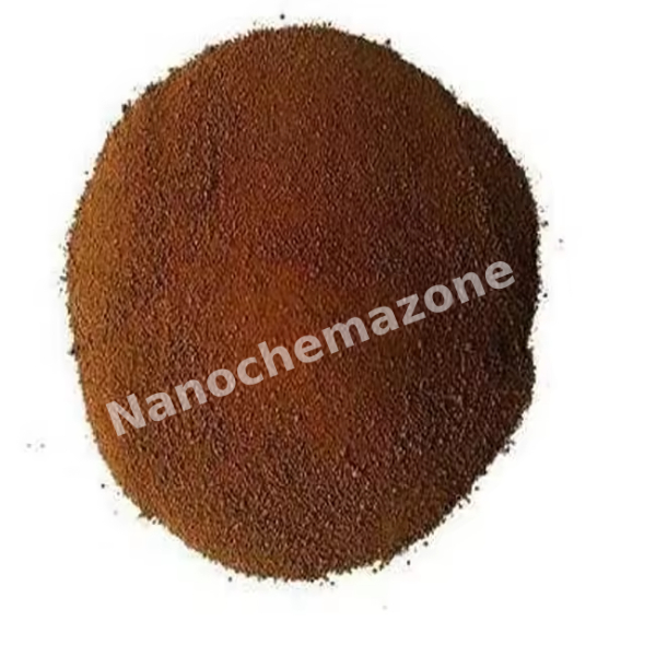
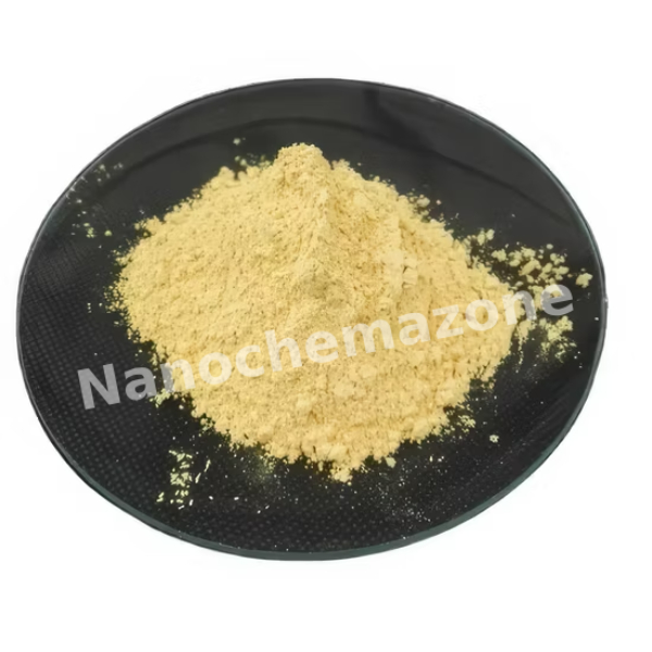
Lanthanum Nickel Oxide (LaNiO3) Sputtering Targets, Purity: 99.9%, Size: 6”, Thickness: 0.250”

$1,245.00

Product 

Lanthanum Nickel Oxide (LaNiO3) Sputtering Targets, Purity: 99.9%, Size: 6'', Thickness: 0.250''

CAS No.

12031‑18‑4

Appearance

Powder

Purity

≥99%,  ≥99.9%,  ≥95%

(Other purities are also available)

APS

 ~1–5 µm (Size Can be customized), Ask for other available size ranges.

Ingredient

N/A

Molecular Weight

 ~245.6 g/mol

Melting Point

Decomposes at ~1300–1500 °C

Boiling Point

N/A

Density

 ~6.5–7.0 g/cm³

Product Codes

NCZ-2116K

Nickel Oxide (NiO) Sputtering Targets, indium, Purity: 99.98%, Size: 2”, Thickness: 0.125”

$1,249.00

Product 

Nickel Oxide (NiO) Sputtering Targets, indium, Purity: 99.98%, Size: 2'', Thickness: 0.125''

CAS No.

1313-99-1

Appearance

Powder

Purity

≥99%,  ≥99.9%,  ≥95%

(Other purities are also available)

APS

 ~3–5 µm (Size Can be customized), Ask for other available size ranges.

Ingredient

N/A

Molecular Weight

74.69 g/mol

Melting Point

1,950 °C

Boiling Point

 2,730 °C

Density

 6.67 g/cm³

Product Codes

NCZ-1833K

Lanthanum Manganate (LaMnO3) Sputtering Targets, Purity: 99.9%, Size: 4”, Thickness: 0.250”

$1,250.00

Applications of Sputtering Targets;

  • Sputtering targets is used for film deposition. The deposition made by sputter targets is a method of depositing thin films by sputtering that involves eroding material from a "target" source onto a "substrate" such as  a silicon wafer.
  • Semiconductor sputtering targets is used to etch the target. Sputter etching is chosen in cases where a high degree of etching anisotropy is needed and selectivity is not a concern.
  • Sputter targets is also used for analysis by etching away the target material.
One of the example occurs in secondary ion spectroscopy (SIMS), where the target sample is sputtered at a constant rate. As the target is sputtered, the concentration and identity of sputtered atoms are measured using mass spectrometry. By helping of the sputtering target, the composition of the target material can be determined and even extremely low concentrations of impurities are detected. Sputtering target has also application area in space. Sputtering is one of the forms of space weathering, a process that changes the physical and chemical properties of airless bodies, such as asteroids and the Moon.

Lanthanum Nickel Oxide (LaNiO3) Sputtering Targets, Purity: 99.9%, Size: 3”, Thickness: 0.250”

$1,250.00

Applications of Sputtering Targets;

  • Sputtering targets is used for film deposition. The deposition made by sputter targets is a method of depositing thin films by sputtering that involves eroding material from a "target" source onto a "substrate" such as  a silicon wafer.
  • Semiconductor sputtering targets is used to etch the target. Sputter etching is chosen in cases where a high degree of etching anisotropy is needed and selectivity is not a concern.
  • Sputter targets is also used for analysis by etching away the target material.
One of the example occurs in secondary ion spectroscopy (SIMS), where the target sample is sputtered at a constant rate. As the target is sputtered, the concentration and identity of sputtered atoms are measured using mass spectrometry. By helping of the sputtering target, the composition of the target material can be determined and even extremely low concentrations of impurities are detected. Sputtering target has also application area in space. Sputtering is one of the forms of space weathering, a process that changes the physical and chemical properties of airless bodies, such as asteroids and the Moon. Lanthanum nickel oxide with the chemical formula of LaNiO3 is an important perovskite-type oxide with metallic conductivity. Lanthanum nickel oxide is a ternary compound with unique chemical and physical properties. It shows an extended range of oxygen-deficient compositions, an uncommon intrinsic n-type metallic conductance, a perovskite crystal structure and thermal and chemical stability. These characteristics make LNO a technologically important perovskite oxide electrode in many potential applications such as ferroelectric thin film capacitors, solid oxide fuel cells, nonvolatile ferroelectric random access memories and multilayer actuators. Furthermore, LNO films have potential to be used as oxygen pressure and ethanol active sensing layers. Also, the reduced La–Ni mixed oxides are reported to be good catalyst precursors to synthesized organic compounds and to grow large amounts of regular diameter distribution controlled carbon nanotubes. Different chemical and physical thin film deposition techniques have been used to prepare LNO on various substrates. Chemical methods such as chemical vapor deposition, metallo-organic chemical vapor deposition and chemical solution deposition have been used to prepare LNO films. Physical methods such as sputtering, pulsed laser deposition and mist plasma evaporation have also been reported. Wet chemical solution deposition techniques provide simple and versatile alternative methods for thin film preparation.

Bismuth Ferrite (BiFeO3) Sputtering Targets, Purity: 99.9%, Size: 7”, Thickness: 0.250”

$1,250.00

Applications of Sputtering Targets;

Film deposition is accomplished using sputtering targets. A technique for sputtering thin films is called "deposition made by sputter targets," which entails eroding material from a "target" source onto a "substrate" like a silicon wafer. Etching of the target is done using semiconductor sputtering targets. When selectivity is not an issue and a high degree of etching anisotropy is required, sputter etching is the method of choice. By removing the target material through etching, sputter targets are also utilized for investigation. In secondary ion spectroscopy (SIMS), one example is when the target material is sputtered at a steady pace. Mass spectrometry is used to quantify the concentration and identity of spewed atoms as the target is sputtered. With the sputtering target's assistance, the

Mass spectrometry is used to measure and identify individual atoms. The target material's composition may be ascertained and even very low concentrations of contaminants can be found with the aid of the sputtering target.

There is also an application area for sputtering targets in space. One type of space weathering that alters the chemical and physical characteristics of airless worlds like the Moon and asteroids is sputtering.

Lanthanum Manganate (LaMnO3) Sputtering Targets, Purity: 99.9%, Size: 4”, Thickness: 0.250”

$1,250.00

Applications of Sputtering Targets;

Film deposition is accomplished using sputtering targets. A technique for sputtering thin films is called "deposition made by sputter targets," which entails eroding material from a "target" source onto a "substrate" like a silicon wafer. Etching of the target is done using semiconductor sputtering targets. When selectivity is not an issue and a high degree of etching anisotropy is required, sputter etching is the method of choice. By removing the target material through etching, sputter targets are also utilized for investigation. In secondary ion spectroscopy (SIMS), one example is when the target material is sputtered at a steady pace. Mass spectrometry is used to quantify the concentration and identity of spewed atoms as the target is sputtered.

The target material's composition may be ascertained and even very low concentrations of contaminants can be found with the aid of the sputtering target.

There is also an application area for sputtering targets in space. One type of space weathering that alters the chemical and physical characteristics of airless worlds like the Moon and asteroids is sputtering.

Lanthanum Manganate (LaMnO3) Sputtering Targets, Purity: 99.9%, Size: 4”, Thickness: 0.250”

$1,250.00

Applications of Sputtering Targets;

Film deposition is accomplished using sputtering targets. A technique for sputtering thin films is called "deposition made by sputter targets," which entails eroding material from a "target" source onto a "substrate" like a silicon wafer. Etching of the target is done using semiconductor sputtering targets. When selectivity is not an issue and a high degree of etching anisotropy is required, sputter etching is the method of choice. By removing the target material through etching, sputter targets are also utilized for investigation. In secondary ion spectroscopy (SIMS), one example is when the target material is sputtered at a steady pace. Mass spectrometry is used to quantify the concentration and identity of spewed atoms as the target is sputtered.

The target material's composition may be ascertained and even very low concentrations of contaminants can be found with the aid of the sputtering target.

There is also an application area for sputtering targets in space. One type of space weathering that alters the chemical and physical characteristics of airless worlds like the Moon and asteroids is sputtering.

Barium Titanate (BaTiO3) Sputtering Targets, Purity: 99.99%, Size: 4”, Thickness: 0.250”

$1,250.00

Product 

Barium Titanate (BaTiO3) Sputtering Targets, Purity: 99.99%, Size: 4'', Thickness: 0.250''

CAS No.

 12047‑27‑7

Appearance

Powder

Purity

≥99%,  ≥99.9%,  ≥95%

(Other purities are also available)

APS

1 – 5 µm (Size Can be customized), Ask for other available size ranges.

Ingredient

N/A

Molecular Weight

~233.19 g/mol

Melting Point

~1625 °C

Boiling Point

N/A

Density

 ~6.02 g/cm³

Product Codes

NCZ-2459K

Praseodymium Calcium Manganate (Pr0.7Ca0.3MnO3) Sputtering Targets, Purity: 99.9%, Size: 3”, Thickness: 0.250”

$1,251.00

Product 

Praseodymium Calcium Manganate (Pr0.7Ca0.3MnO3) Sputtering Targets, Purity: 99.9%, Size: 3'', Thickness: 0.250''

CAS No.

N/A

Appearance

Powder

Purity

≥99%,  ≥99.9%,  ≥95%

(Other purities are also available)

APS

1–5 μm (Size Can be customized), Ask for other available size ranges.

Ingredient

N/A

Molecular Weight

237.66 g/mol

Melting Point

N/A

Boiling Point

N/A

Density

~6.4–6.8 g/cm³

Product Codes

NCZ-1778K

Zinc Sulfide (ZnS) Sputtering Targets, indium, Purity: 99.99%, Size: 3”, Thickness: 0.125”

$1,252.00

Product 

Zinc Sulfide (ZnS) Sputtering Targets, indium, Purity: 99.99%, Size: 3'', Thickness: 0.125''

CAS No.

1314-98-3

Appearance

Powder

Purity

≥99%,  ≥99.9%,  ≥95%

(Other purities are also available)

APS

 (ZnS) (Size Can be customized), Ask for other available size ranges.

Ingredient

N/A

Molecular Weight

97.45 g/mol

Melting Point

~1700 °C

Boiling Point

N/A

Density

 4.09 g/cm³

Product Codes

NCZ-1500K

Cerium Oxide (CeO2) Sputtering Targets, Purity: 99.99%, Size: 4”, Thickness: 0.125”

$1,255.00

Applications of Sputtering Targets;

Film deposition is accomplished using sputtering targets. A technique for sputtering thin films is called "deposition made by sputter targets," which entails eroding material from a "target" source onto a "substrate" like a silicon wafer. Etching of the target is done using semiconductor sputtering targets. When selectivity is not an issue and a high degree of etching anisotropy is required, sputter etching is the method of choice. By removing the target material through etching, sputter targets are also utilized for investigation. In secondary ion spectroscopy (SIMS), one example is when the target material is sputtered at a steady pace. Mass spectrometry is used to quantify the concentration and identity of spewed atoms as the target is sputtered.

The target material's composition may be ascertained and even very low concentrations of contaminants can be found with the aid of the sputtering target.

There is also an application area for sputtering targets in space. One type of space weathering that alters the chemical and physical characteristics of airless worlds like the Moon and asteroids is sputtering.

The most prevalent rare-earth element in the crust of the earth is cerium, a metal that belongs to the lanthanide series. Cerium oxide's high refractive index and dielectric constant make it suitable for a wide range of optical and electrical applications. Additionally, cerium oxide can be used for corrosion protection coatings rather than coatings based on chromate.

Lanthanum Nickel Oxide (LaNiO3) Sputtering Targets, Purity: 99.9%, Size: 6”, Thickness: 0.125”

$1,256.00

Applications of Sputtering Targets;

  • Sputtering targets is used for film deposition. The deposition made by sputter targets is a method of depositing thin films by sputtering that involves eroding material from a "target" source onto a "substrate" such as  a silicon wafer.
  • Semiconductor sputtering targets is used to etch the target. Sputter etching is chosen in cases where a high degree of etching anisotropy is needed and selectivity is not a concern.
  • Sputter targets is also used for analysis by etching away the target material.
One of the example occurs in secondary ion spectroscopy (SIMS), where the target sample is sputtered at a constant rate. As the target is sputtered, the concentration and identity of sputtered atoms are measured using mass spectrometry. By helping of the sputtering target, the composition of the target material can be determined and even extremely low concentrations of impurities are detected. Sputtering target has also application area in space. Sputtering is one of the forms of space weathering, a process that changes the physical and chemical properties of airless bodies, such as asteroids and the Moon. Lanthanum nickel oxide with the chemical formula of LaNiO3 is an important perovskite-type oxide with metallic conductivity. Lanthanum nickel oxide is a ternary compound with unique chemical and physical properties. It shows an extended range of oxygen-deficient compositions, an uncommon intrinsic n-type metallic conductance, a perovskite crystal structure and thermal and chemical stability. These characteristics make LNO a technologically important perovskite oxide electrode in many potential applications such as ferroelectric thin film capacitors, solid oxide fuel cells, nonvolatile ferroelectric random access memories and multilayer actuators. Furthermore, LNO films have potential to be used as oxygen pressure and ethanol active sensing layers. Also, the reduced La–Ni mixed oxides are reported to be good catalyst precursors to synthesized organic compounds and to grow large amounts of regular diameter distribution controlled carbon nanotubes. Different chemical and physical thin film deposition techniques have been used to prepare LNO on various substrates. Chemical methods such as chemical vapor deposition, metallo-organic chemical vapor deposition and chemical solution deposition have been used to prepare LNO films. Physical methods such as sputtering, pulsed laser deposition and mist plasma evaporation have also been reported. Wet chemical solution deposition techniques provide simple and versatile alternative methods for thin film preparation.

Lithium Phosphate (Li3PO4) Sputtering Targets, Purity: 99.95%, Size: 4”, Thickness: 0.250”

$1,256.00

Applications of Sputtering Targets;

Film deposition is accomplished using sputtering targets. A technique for sputtering thin films is called "deposition made by sputter targets," which entails eroding material from a "target" source onto a "substrate" like a silicon wafer. Etching of the target is done using semiconductor sputtering targets. When selectivity is not an issue and a high degree of etching anisotropy is required, sputter etching is the method of choice. By removing the target material through etching, sputter targets are also utilized for investigation. In secondary ion spectroscopy (SIMS), one example is when the target material is sputtered at a steady pace. Mass spectrometry is used to quantify the concentration and identity of spewed atoms as the target is sputtered.

By helping of the sputtering target, the composition of the target material may be evaluated and even extremely tiny amounts of contaminants are recognized.

There is also an application area for sputtering targets in space. One type of space weathering that alters the chemical and physical characteristics of airless worlds like the Moon and asteroids is sputtering.

Lithium Phosphate (Li3PO4) Sputtering Targets, Purity: 99.95%, Size: 5”, Thickness: 0.250”

$1,257.00

Applications of Sputtering Targets;

Film deposition is accomplished using sputtering targets. A technique for sputtering thin films is called "deposition made by sputter targets," which entails eroding material from a "target" source onto a "substrate" like a silicon wafer. Etching of the target is done using semiconductor sputtering targets. When etching anisotropy is high, sputter etching is the preferred method.

is required, and selectivity is unimportant. By removing the target material through etching, sputter targets are also utilized for investigation. In secondary ion spectroscopy (SIMS), one example is when the target material is sputtered at a steady pace. Mass spectrometry is used to quantify the concentration and identity of spewed atoms as the target is sputtered.

By helping of the sputtering target, the composition of the target material may be evaluated and even extremely tiny amounts of contaminants are recognized.

There is also an application area for sputtering targets in space. One type of space weathering that alters the chemical and physical characteristics of airless worlds like the Moon and asteroids is sputtering.

Silicon Carbide (SiC) Sputtering Targets, indium, Purity: 99.5%, Size: 4”, Thickness: 0.125”

$1,261.00

Product 

Silicon Carbide (SiC) Sputtering Targets, indium, Purity: 99.5%, Size: 4'', Thickness: 0.125''

CAS No.

 409-21-2

Appearance

Powder

Purity

≥99%,  ≥99.9%,  ≥95%

(Other purities are also available)

APS

N/A  (Size Can be customized), Ask for other available size ranges.

Ingredient

N/A

Molecular Weight

 40.10 g/mol

Melting Point

~2,700 °C

Boiling Point

N/A

Density

~3.21 g/cm³

Product Codes

NCZ-1720K

La-substituted Bismuth Ferrite Sputtering Target Bi0.85La0.15FeO3

$1,262.00
Select options This product has multiple variants. The options may be chosen on the product page
Product La-substituted Bismuth Ferrite Sputtering Target Bi0.85La0.15FeO3
CAS No. 12010-42-3
Appearance Gray ceramic targets
Purity ≥99%,  ≥99.9%,  ≥95%(Other purities are also available)
APS N/A
Ingredient Bi0.85La0.15FeO3
Molecular Weight N/A
Melting Point N/A
Boiling Point N/A
Density N/A
Product Codes NCZ-123H

Nickel Oxide (NiO) Sputtering Targets, indium, Purity: 99.95%, Size: 2”, Thickness: 0.125”

$1,266.00

Product 

Nickel Oxide (NiO) Sputtering Targets, indium, Purity: 99.95%, Size: 2'', Thickness: 0.125''

CAS No.

1313-99-1

Appearance

Powder

Purity

≥99%,  ≥99.9%,  ≥95%

(Other purities are also available)

APS

 ~3–5 µm (Size Can be customized), Ask for other available size ranges.

Ingredient

N/A

Molecular Weight

74.69 g/mol

Melting Point

1,950 °C

Boiling Point

 2,730 °C

Density

 6.67 g/cm³

Product Codes

NCZ-1832K

Tungsten Oxide (WO3) Sputtering Targets, Purity: 99.9%, Size: 2”, Thickness: 0.250”

$1,272.00

Product 

Tungsten Oxide (WO3) Sputtering Targets, Purity: 99.9%, Size: 2'', Thickness: 0.250''

CAS No.

1314-35-8

Appearance

Powder

Purity

≥99%,  ≥99.9%,  ≥95%

(Other purities are also available)

APS

N/A  (Size Can be customized), Ask for other available size ranges.

Ingredient

N/A

Molecular Weight

231.84 g/mol

Melting Point

1,473 °C

Boiling Point

1,700–1,850 °C

Density

7.16 g/cm³

Product Codes

NCZ-1571K

Barium Zirconate (BaZrO3) Sputtering Targets, Purity: 99.99%, Size: 4”, Thickness: 0.250”

$1,275.00

Applications of Sputtering Targets;

Film deposition is accomplished using sputtering targets. A technique for sputtering thin films is called "deposition made by sputter targets," which entails eroding material from a "target" source onto a "substrate" like a silicon wafer. Etching of the target is done using semiconductor sputtering targets. When selectivity is not an issue and a high degree of etching anisotropy is required, sputter etching is the method of choice. By removing the target material through etching, sputter targets are also utilized for investigation. In secondary ion spectroscopy (SIMS), one example is when the target material is sputtered at a steady pace. Mass spectrometry is used to quantify the concentration and identity of spewed atoms as the target is sputtered. With the sputtering target's assistance, the

It is possible to identify the target material's composition and even detect incredibly low impurity quantities.

There is also an application area for sputtering targets in space. One type of space weathering that alters the chemical and physical characteristics of airless worlds like the Moon and asteroids is sputtering.

The chemical compound barium zirconate has the formula BaZrO3. An electroceramic, or family of ceramic materials principally employed for their electrical capabilities, is what barium zirconate is. Applications for barium zirconate sputtering targets include semiconductors, photonic, and physical and chemical vapor deposition (PVD) as well as CVD and PVD displays. Barium zirconate sputtering targets can also be employed for ferroelectric applications.

NH2 Modified Upconverting Nanoparticles Water Solution, 10mg/bottle

$1,276.00
Select options This product has multiple variants. The options may be chosen on the product page
Product NH2 Modified Upconverting Nanoparticles Water Solution, 10mg/bottle
CAS No. N/A
Appearance Clear to slightly opalescent
Purity ≥99%,  ≥99.9%,  ≥95%(Other purities are also available)
APS 20–50nm ( (Size Can be customized),  Ask for other available size range.
Ingredient NaYF₄
Molecular Weight 188 g/mol
Melting Point N/A
Boiling Point N/A
Density 4.2–4.3 g/cm³
Product Codes NCZ-475I

Upconverting Nanoparticles Water Solution, 10mg/bottle

$1,276.00
Select options This product has multiple variants. The options may be chosen on the product page
Product Upconverting Nanoparticles Water Solution, 10mg/bottle
CAS No. N/A
Appearance Ivory-white to pale color
Purity ≥99%,  ≥99.9%,  ≥95%(Other purities are also available)
APS 25nm (Size Can be customized),  Ask for other available size range.
Ingredient NaYF₄:Yb³⁺,Er³⁺
Molecular Weight N/A
Melting Point N/A
Boiling Point N/A
Density N/A
Product Codes NCZ-591I

Cerium Oxide (CeO2) Sputtering Targets, Purity: 99.99%, Size: 3”, Thickness: 0.250”

$1,277.00

Applications of Sputtering Targets;

Film deposition is accomplished using sputtering targets. A technique for sputtering thin films is called "deposition made by sputter targets," which entails eroding material from a "target" source onto a "substrate" like a silicon wafer. Etching of the target is done using semiconductor sputtering targets. When selectivity is not an issue and a high degree of etching anisotropy is required, sputter etching is the method of choice. By removing the target material through etching, sputter targets are also utilized for investigation. In secondary ion spectroscopy (SIMS), one example is when the target material is sputtered at a steady pace. Mass spectrometry is used to quantify the concentration and identity of spewed atoms as the target is sputtered.

The target material's composition may be ascertained and even very low concentrations of contaminants can be found with the aid of the sputtering target.

There is also an application area for sputtering targets in space. One type of space weathering that alters the chemical and physical characteristics of airless worlds like the Moon and asteroids is sputtering.

The most prevalent rare-earth element in the crust of the earth is cerium, a metal that belongs to the lanthanide series. Cerium oxide's high refractive index and dielectric constant make it suitable for a wide range of optical and electrical applications. Additionally, cerium oxide can be used for corrosion protection coatings rather than coatings based on chromate.

Tungsten Oxide (WO3) Sputtering Targets, Purity: 99.9%, Size: 3”, Thickness: 0.125”

$1,279.00

Product 

Tungsten Oxide (WO3) Sputtering Targets, Purity: 99.9%, Size: 3'', Thickness: 0.125''

CAS No.

1314-35-8

Appearance

Powder

Purity

≥99%,  ≥99.9%,  ≥95%

(Other purities are also available)

APS

N/A  (Size Can be customized), Ask for other available size ranges.

Ingredient

N/A

Molecular Weight

231.84 g/mol

Melting Point

1,473 °C

Boiling Point

1,700–1,850 °C

Density

7.16 g/cm³

Product Codes

NCZ-1570K

Barium Titanate (BaTiO3) Sputtering Targets, elastomer, Purity: 99.99%, Size: 4”, Thickness: 0.125”

$1,281.00

Applications of Sputtering Targets;

Film deposition is accomplished using sputtering targets. A technique for sputtering thin films is called "deposition made by sputter targets," which entails eroding material from a "target" source onto a "substrate" like a silicon wafer. Etching of the target is done using semiconductor sputtering targets. When selectivity is not an issue and a high degree of etching anisotropy is required, sputter etching is the method of choice. By removing the target material through etching, sputter targets are also utilized for investigation. In secondary ion spectroscopy (SIMS), one example is when the target material is sputtered at a steady pace. Mass spectrometry is used to quantify the concentration and identity of spewed atoms as the target is sputtered. With the sputtering target's assistance, the

There is also an application area for sputtering targets in space. One type of space weathering that alters the chemical and physical characteristics of airless worlds like the Moon and asteroids is sputtering.

Formulated as BaTiO3, barium titanate is an inorganic substance. When formed as big crystals, barium titanate is clear and has a white powdery appearance. It is a ferroelectric ceramic material with piezoelectric and photorefractive characteristics. The applications of barium titanate sputtering agents are numerous. For instance, barium titanate films, which are produced by sputtering targets, can be employed in particular electronic ceramics. Barium titanate can be utilized in the building of electrical devices such as sensors, capacitors, and detectors.

Magnesium Oxide (MgO) Sputtering Targets, indium, Purity: 99.95%, Size: 3”, Thickness: 0.125”

$1,282.00

Applications of Sputtering Targets;

Film deposition is accomplished using sputtering targets. A technique for sputtering thin films is called "deposition made by sputter targets," which entails eroding material from a "target" source onto a "substrate" like a silicon wafer. Etching of the target is done using semiconductor sputtering targets. When selectivity is not an issue and a high degree of etching anisotropy is required, sputter etching is the method of choice. By removing the target material through etching, sputter targets are also utilized for investigation. In secondary ion spectroscopy (SIMS), one example is when the target material is sputtered at a steady pace. Mass spectrometry is used to quantify the concentration and identity of spewed atoms as the target is sputtered.

By helping of the sputtering target, the composition of the target material may be evaluated and even extremely tiny amounts of contaminants are recognized.

There is also an application area for sputtering targets in space. One type of space weathering that alters the chemical and physical characteristics of airless worlds like the Moon and asteroids is sputtering.

Cerium Oxide (CeO2) Sputtering Targets, Purity: 99.99%, Size: 5”, Thickness: 0.125”

$1,284.00

Product 

Cerium Oxide (CeO2) Sputtering Targets, Purity: 99.99%, Size: 5'', Thickness: 0.125''

CAS No.

 1306-38-3

Appearance

Powder

Purity

≥99%,  ≥99.9%,  ≥95%

(Other purities are also available)

APS

 N/A (Size Can be customized), Ask for other available size ranges.

Ingredient

N/A

Molecular Weight

 172.11 g/mol

Melting Point

2,400–2,600 °C

Boiling Point

Sublimes above 3,000 °C

Density

 7.13 g/cm³

Product Codes

NCZ-2326K

Lanthanum Nickel Oxide (LaNiO3) Sputtering Targets, Purity: 99.9%, Size: 1”, Thickness: 0.125”

$1,286.00

Product 

Lanthanum Nickel Oxide (LaNiO3) Sputtering Targets, Purity: 99.9%, Size: 1'', Thickness: 0.125''

CAS No.

12031‑18‑4

Appearance

Powder

Purity

≥99%,  ≥99.9%,  ≥95%

(Other purities are also available)

APS

 ~1–5 µm (Size Can be customized), Ask for other available size ranges.

Ingredient

N/A

Molecular Weight

 ~245.6 g/mol

Melting Point

Decomposes at ~1300–1500 °C

Boiling Point

N/A

Density

 ~6.5–7.0 g/cm³

Product Codes

NCZ-2127K

Iron Oxide (Fe3O4) Sputtering Targets, indium, Purity: 99.9%, Size: 3”, Thickness: 0.125”

$1,287.00

Product 

Iron Oxide (Fe3O4) Sputtering Targets, indium, Purity: 99.9%, Size: 3'', Thickness: 0.125''

CAS No.

1317‑61‑9

Appearance

Powder

Purity

≥99%,  ≥99.9%,  ≥95%

(Other purities are also available)

APS

 N/A (Size Can be customized), Ask for other available size ranges.

Ingredient

N/A

Molecular Weight

 231.6 g/mol

Melting Point

~1,597 °C

Boiling Point

 ~2,623 °C (material may decompose before boiling)

Density

 ~5.17 g/cm³ (sintered target)

Product Codes

NCZ-2161K

Lanthanum Nickel Oxide (LaNiO3) Sputtering Targets, Purity: 99.9%, Size: 1”, Thickness: 0.250”

$1,291.00

Product 

Lanthanum Nickel Oxide (LaNiO3) Sputtering Targets, Purity: 99.9%, Size: 1'', Thickness: 0.250''

CAS No.

12031‑18‑4

Appearance

Powder

Purity

≥99%,  ≥99.9%,  ≥95%

(Other purities are also available)

APS

 ~1–5 µm (Size Can be customized), Ask for other available size ranges.

Ingredient

N/A

Molecular Weight

 ~245.6 g/mol

Melting Point

Decomposes at ~1300–1500 °C

Boiling Point

N/A

Density

 ~6.5–7.0 g/cm³

Product Codes

NCZ-2126K

Lanthanum Manganate (LaMnO3) Sputtering Targets, Purity: 99.9%, Size: 7”, Thickness: 0.125”

$1,291.00

Product 

Lanthanum Manganate (LaMnO3) Sputtering Targets, Purity: 99.9%, Size: 7'', Thickness: 0.125''

CAS No.

13538-87-7

Appearance

Powder

Purity

≥99%,  ≥99.9%,  ≥95%

(Other purities are also available)

APS

 ~1–5 µm (Size Can be customized), Ask for other available size ranges.

Ingredient

N/A

Molecular Weight

240.83 g/mol

Melting Point

 ~2300 °C

Boiling Point

N/A

Density

~6.3 – 6.8 g/cm³

Product Codes

NCZ-2131K

Magnesium Oxide (MgO) Sputtering Targets, Purity: 99.95%, Size: 8”, Thickness: 0.125”

$1,294.00

Product 

Magnesium Oxide (MgO) Sputtering Targets, Purity: 99.95%, Size: 8'', Thickness: 0.125''

CAS No.

1309-48-4

Appearance

Powder

Purity

≥99%,  ≥99.9%,  ≥95%

(Other purities are also available)

APS

 N/A (Size Can be customized), Ask for other available size ranges.

Ingredient

N/A

Molecular Weight

40.30 g/mol

Melting Point

 ~2852 °C

Boiling Point

~3600 °C

Density

 ~3.58 g/cm³

Product Codes

NCZ-1962K

Magnesium Fluoride (MgF2) Sputtering Targets, Purity: 99.9%, Size: 8”, Thickness: 0.250”

$1,294.00

Product 

Magnesium Fluoride (MgF2) Sputtering Targets, Purity: 99.9%, Size: 8'', Thickness: 0.250''

CAS No.

7783-40-6

Appearance

Powder

Purity

≥99%,  ≥99.9%,  ≥95%

(Other purities are also available)

APS

 N/A (Size Can be customized), Ask for other available size ranges.

Ingredient

N/A

Molecular Weight

 62.30 g/mol

Melting Point

~1263 °C

Boiling Point

~2260 °C

Density

 3.18 g/cm³

Product Codes

NCZ-1977K

Molybdenum Disilicide (MoSi2) Sputtering Targets, indium, Purity: 99.95%, Size: 4”, Thickness: 0.125”

$1,296.00

Product 

Molybdenum Disilicide (MoSi2) Sputtering Targets, indium, Purity: 99.95%, Size: 4'', Thickness: 0.125''

CAS No.

12136-78-6

Appearance

Powder

Purity

≥99%,  ≥99.9%,  ≥95%

(Other purities are also available)

APS

 N/A (Size Can be customized), Ask for other available size ranges.

Ingredient

N/A

Molecular Weight

152.11 g/mol

Melting Point

 ~2030 °C

Boiling Point

 ~2300 °C to 2500 °C

Density

~6.26 g/cm³

Product Codes

NCZ-1920K

Lanthanum Strontium Manganate (La0.7Sr0.3MnO3) Sputtering Targets, Purity: 99.9%, Size: 4”, Thickness: 0.125”

$1,298.00

Applications of Sputtering Targets;

  • Sputtering targets is used for film deposition. The deposition made by sputter targets is a method of depositing thin films by sputtering that involves eroding material from a "target" source onto a "substrate" such as  a silicon wafer.
  • Semiconductor sputtering targets is used to etch the target. Sputter etching is chosen in cases where a high degree of etching anisotropy is needed and selectivity is not a concern.
  • Sputter targets is also used for analysis by etching away the target material.
One of the example occurs in secondary ion spectroscopy (SIMS), where the target sample is sputtered at a constant rate. As the target is sputtered, the concentration and identity of sputtered atoms are measured using mass spectrometry. By helping of the sputtering target, the composition of the target material can be determined and even extremely low concentrations of impurities are detected. Sputtering target has also application area in space. Sputtering is one of the forms of space weathering, a process that changes the physical and chemical properties of airless bodies, such as asteroids and the Moon.

Cerium Oxide (CeO2) Sputtering Targets, Purity: 99.99%, Size: 6”, Thickness: 0.125”

$1,300.00

Applications of Sputtering Targets;

Film deposition is accomplished using sputtering targets. A technique for sputtering thin films is called "deposition made by sputter targets," which entails eroding material from a "target" source onto a "substrate" like a silicon wafer. Etching of the target is done using semiconductor sputtering targets. When selectivity is not an issue and a high degree of etching anisotropy is required, sputter etching is the method of choice. By removing the target material through etching, sputter targets are also utilized for investigation. In secondary ion spectroscopy (SIMS), one example is when the target material is sputtered at a steady pace. Mass spectrometry is used to quantify the concentration and identity of spewed atoms as the target is sputtered.

The target material's composition may be ascertained and even very low concentrations of contaminants can be found with the aid of the sputtering target.

There is also an application area for sputtering targets in space. One type of space weathering that alters the chemical and physical characteristics of airless worlds like the Moon and asteroids is sputtering.

The most prevalent rare-earth element in the crust of the earth is cerium, a metal that belongs to the lanthanide series. Cerium oxide's high refractive index and dielectric constant make it suitable for a wide range of optical and electrical applications. Additionally, cerium oxide can be used for corrosion protection coatings rather than coatings based on chromate.

Lithium Phosphate (Li3PO4) Sputtering Targets, Purity: 99.95%, Size: 4”, Thickness: 0.125”

$1,300.00

Product 

Lithium Phosphate (Li3PO4) Sputtering Targets, Purity: 99.95%, Size: 4'', Thickness: 0.125''

CAS No.

10377-52-3

Appearance

Powder

Purity

≥99%,  ≥99.9%,  ≥95%

(Other purities are also available)

APS

 N/A (Size Can be customized), Ask for other available size ranges.

Ingredient

N/A

Molecular Weight

 115.79 g/mol

Melting Point

 ~837 °C

Boiling Point

~158 °C (likely decomposition)

Density

 ~2.53 g/cm³

Product Codes

NCZ-2029K

Gallium Antimonide (GaSb) Wafers, Size: 4”, Thickness: 1000± 25 μm, Orientation: 111, EPI-Ready (No reviews yet)

Price range: $1,301.00 through $5,392.00
Select options This product has multiple variants. The options may be chosen on the product page
1 piece/1180 € 5 pieces/4890 €                         Please contact us for quotes on larger quantities !!!

Gallium Antimonide (GaSb) Wafers

Size: 4”, Thickness: 1000± 25 μm, Orientation: 111

Technical Properties:

Quality  EPI-Ready
Size (inch)  4”
Thickness (μm)  1000± 25
Polished  Single Side
Dopant  Tellurium ( N type )
Orientation  111
Mobility  2000-3500
EPD  ≤2000
Growth method  VGF
OF Length  32.5±2
IF Length   18±1

Fields of Application for Gallium Antimonide (GaSb)

The intermetallic compound of gallium antimonide (GaSb) was first prepared in 1926 by Victor Goldschmidt. Gallium antimonide (GaSb) is a semiconductor made of gallium and antimony of the group III-V compounds. Gallium antimonide (GaSb) is supplied in polished wafer form. Gallium antimonide (GaSb) wafers are produced from polycrystalline ingots with using Czochralski method to obtain a single crystal with perfect purity. Supplied in polished wafer form, gallium antimonide has a very high accuracy of orientation. Thickness and orientation of these wafers can be modified with additives. Czochralski method is used to provide the growh of pure gallium and antimonide elements. The natural low-defect structure of GaSb makes it a perfect material for epitaxial growth. They are supplied in polished 1 side or 2 sides and cut forms.
  • Gallium antimonide (GaSb) is used for infrared detectors.
  • Gallium antimonide (GaSb) is used for infrared LEDs.
  • Gallium antimonide (GaSb) is used for transistors.
  • Gallium antimonide (GaSb) is used for lasers.
  • Gallium antimonide (GaSb) is used for thermophotovoltaic systems.

Gallium Antimonide (GaSb) Wafers, Size: 4”, Thickness: 1000± 25 μm, Orientation: 100, EPI-Ready

Price range: $1,301.00 through $5,392.00
Select options This product has multiple variants. The options may be chosen on the product page
1 piece/1180 € 5 pieces/4890 €                           Please contact us for quotes on larger quantities !!!

Gallium Antimonide (GaSb) Wafers

Size: 4”, Thickness: 1000± 25 μm, Orientation: 111

Technical Properties:

Quality  EPI-Ready
Size (inch)  4”
Thickness (μm)  1000± 25
Polished  Single Side
Dopant  Tellurium ( N type )
Orientation  100
Mobility  2000-3500
EPD  ≤2000
Growth method  VGF
OF Length  32.5±2
IF Length   18±1

Fields of Application for Gallium Antimonide (GaSb)

The intermetallic compound of gallium antimonide (GaSb) was first prepared in 1926 by Victor Goldschmidt. Gallium antimonide (GaSb) is a semiconductor made of gallium and antimony of the group III-V compounds. Gallium antimonide (GaSb) is supplied in polished wafer form. Gallium antimonide (GaSb) wafers are produced from polycrystalline ingots with using Czochralski method to obtain a single crystal with perfect purity. Supplied in polished wafer form, gallium antimonide has a very high accuracy of orientation. Thickness and orientation of these wafers can be modified with additives. Czochralski method is used to provide the growh of pure gallium and antimonide elements. The natural low-defect structure of GaSb makes it a perfect material for epitaxial growth. They are supplied in polished 1 side or 2 sides and cut forms.
  • Gallium antimonide (GaSb) is used for infrared detectors.
  • Gallium antimonide (GaSb) is used for infrared LEDs.
  • Gallium antimonide (GaSb) is used for transistors.
  • Gallium antimonide (GaSb) is used for lasers.
  • Gallium antimonide (GaSb) is used for thermophotovoltaic systems.

Tantalum Carbide (TaC) Powder (99%)

Price range: $1,304.00 through $37,198.00
Select options This product has multiple variants. The options may be chosen on the product page
Product Tantalum Carbide (TaC) Powder (99%)
CAS No. 12070-06-3
Appearance Gray to black crystalline
Purity ≥99%,  ≥99.9%,  ≥95%(Other purities are also available)
APS 1–10µm (Size Can be customized),  Ask for other available size range.
Ingredient TaC
Molecular Weight 192.96 g/mol
Melting Point 3880 °C
Boiling Point N/A
Density 3.5–5.0 g/cm³
Product Codes NCZ-551I
 

Bismuth Telluride (Bi2Te3) Sputtering Targets, Purity: 99.999%, Size: 3”, Thickness: 0.250”

$1,305.00

Applications of Sputtering Targets;

Film deposition is accomplished using sputtering targets. A technique for sputtering thin films is called "deposition made by sputter targets," which entails eroding material from a "target" source onto a "substrate" like a silicon wafer. Etching of the target is done using semiconductor sputtering targets. When selectivity is not an issue and a high degree of etching anisotropy is required, sputter etching is the method of choice. By removing the target material through etching, sputter targets are also utilized for investigation. In secondary ion spectroscopy (SIMS), one example is when the target material is sputtered at a steady pace. Mass spectrometry is used to quantify the concentration and identity of spewed atoms as the target is sputtered.

The target material's composition may be ascertained and even very low concentrations of contaminants can be found with the aid of the sputtering target.

There is also an application area for sputtering targets in space. One type of space weathering that alters the chemical and physical characteristics of airless worlds like the Moon and asteroids is sputtering.

Bi2Te3, or bismuth telluride, is a gray powder that is a combination of bismuth and tellurium. It is a semiconductor that becomes an effective thermoelectric material for refrigeration or portable power generation when alloyed with antimony or selenium. Since Bi2Te3 is a topological insulator, its physical characteristics depend on its thickness.

Bismuth Ferrite (BiFeO3) Sputtering Targets, Purity: 99.9%, Size: 6”, Thickness: 0.125”

$1,305.00

Product 

Bismuth Ferrite (BiFeO3) Sputtering Targets, Purity: 99.9%, Size: 6'', Thickness: 0.125''

CAS No.

 12010‑42‑3

Appearance

Powder

Purity

≥99%,  ≥99.9%,  ≥95%

(Other purities are also available)

APS

 0.5–2 µm (Size Can be customized), Ask for other available size ranges.

Ingredient

N/A

Molecular Weight

~312.82 g/mol

Melting Point

 ~1255 °C (bulk material)

Boiling Point

N/A

Density

~8.22 g/cm³

Product Codes

NCZ-2421K

Tungsten Oxide (WO3) Sputtering Targets, indium, Purity: 99.9%, Size: 2”, Thickness: 0.125”

$1,308.00

Applications of Sputtering Targets;

For film deposition, sputtering targets are employed. A sputtering technique called "deposition made by sputter targets" entails eroding material from a "target" source onto a "substrate" like a silicon wafer. Targets are etched using semiconductor sputtering targets. When etching anisotropy is required to a great degree and selectivity is not an issue, sputter etching is the method of choice. By etching away the target material, sputter targets are also utilized for investigation. In one instance, the target sample is sputtered at a steady pace in secondary ion spectroscopy (SIMS). Using mass spectrometry, the concentration and identity of the spewed atoms are determined when the target is sputtered.

The target material's composition may be ascertained and even very low concentrations of contaminants can be found with the aid of the sputtering target.

There is also an application area for sputtering targets in space. One type of space weathering that alters the chemical and physical characteristics of airless worlds like the Moon and asteroids is sputtering.

Bismuth Ferrite (BiFeO3) Sputtering Targets, Purity: 99.9%, Size: 8”, Thickness: 0.125”

$1,310.00

Applications of Sputtering Targets;

Film deposition is accomplished using sputtering targets. A technique for sputtering thin films is called "deposition made by sputter targets," which entails eroding material from a "target" source onto a "substrate" like a silicon wafer. Etching of the target is done using semiconductor sputtering targets. When selectivity is not an issue and a high degree of etching anisotropy is required, sputter etching is the method of choice. By removing the target material through etching, sputter targets are also utilized for investigation.

In secondary ion spectroscopy (SIMS), one example is when the target material is sputtered at a steady pace. Mass spectrometry is used to quantify the concentration and identity of spewed atoms as the target is sputtered. The target material's composition may be ascertained and even very low concentrations of contaminants can be found with the aid of the sputtering target.

There is also an application area for sputtering targets in space. One type of space weathering that alters the chemical and physical characteristics of airless worlds like the Moon and asteroids is sputtering. One of the most promising multiferroic materials is bismuth ferrite, an inorganic chemical compound with a perovskite structure and the chemical formula BiFeO3. In order to create a one-phase material called bismuth ferrite (BiFeO3), a bismuth ferrite sputtering target is often manufactured by high temperature sinttering or recrystallizing the mixture of the oxide compound of Bi and Fe. For targets that are sputtering bismuth ferrite, indium bonding is advised.

Lithium Phosphate (Li3PO4) Sputtering Targets, Purity: 99.95%, Size: 5”, Thickness: 0.125”

$1,313.00

Product 

Lithium Phosphate (Li3PO4) Sputtering Targets, Purity: 99.95%, Size: 5'', Thickness: 0.125''

CAS No.

10377-52-3

Appearance

Powder

Purity

≥99%,  ≥99.9%,  ≥95%

(Other purities are also available)

APS

 N/A (Size Can be customized), Ask for other available size ranges.

Ingredient

N/A

Molecular Weight

 115.79 g/mol

Melting Point

 ~837 °C

Boiling Point

N/A

Density

 ~2.53 g/cm³

Product Codes

NCZ-2027K

Barium Strontium Titanate (BaO4SrTi) Sputtering Targets, elastomer, Purity: 99.99%, Size: 3”, Thickness: 0.125”

$1,313.00

Product 

Barium Strontium Titanate (BaO4SrTi) Sputtering Targets, elastomer, Purity: 99.99%, Size: 3'', Thickness: 0.125''

CAS No.

 12060-08-1

Appearance

Powder

Purity

≥99%,  ≥99.9%,  ≥95%

(Other purities are also available)

APS

~1–5 µm (Size Can be customized), Ask for other available size ranges.

Ingredient

N/A

Molecular Weight

~233–300 g/mol (composition dependent)

Melting Point

 ~1625 °C (approximate)

Boiling Point

N/A

Density

~5.5–6.0 g/cm³ (depending on Ba:Sr ratio)

Product Codes

NCZ-2474K

Lanthanum Manganate (LaMnO3) Sputtering Targets, Purity: 99.9%, Size: 5”, Thickness: 0.125”

$1,320.00

Applications of Sputtering Targets;

  • Sputtering targets is used for film deposition. The deposition made by sputter targets is a method of depositing thin films by sputtering that involves eroding material from a "target" source onto a "substrate" such as  a silicon wafer.
  • Semiconductor sputtering targets is used to etch the target. Sputter etching is chosen in cases where a high degree of etching anisotropy is needed and selectivity is not a concern.
  • Sputter targets is also used for analysis by etching away the target material.
One of the example occurs in secondary ion spectroscopy (SIMS), where the target sample is sputtered at a constant rate. As the target is sputtered, the concentration and identity of sputtered atoms are measured using mass spectrometry. By helping of the sputtering target, the composition of the target material can be determined and even extremely low concentrations of impurities are detected. Sputtering target has also application area in space. Sputtering is one of the forms of space weathering, a process that changes the physical and chemical properties of airless bodies, such as asteroids and the Moon.

Lanthanum Nickel Oxide (LaNiO3) Sputtering Targets, Purity: 99.9%, Size: 8”, Thickness: 0.250”

$1,320.00

Applications of Sputtering Targets;

  • Sputtering targets is used for film deposition. The deposition made by sputter targets is a method of depositing thin films by sputtering that involves eroding material from a "target" source onto a "substrate" such as  a silicon wafer.
  • Semiconductor sputtering targets is used to etch the target. Sputter etching is chosen in cases where a high degree of etching anisotropy is needed and selectivity is not a concern.
  • Sputter targets is also used for analysis by etching away the target material.
One of the example occurs in secondary ion spectroscopy (SIMS), where the target sample is sputtered at a constant rate. As the target is sputtered, the concentration and identity of sputtered atoms are measured using mass spectrometry. By helping of the sputtering target, the composition of the target material can be determined and even extremely low concentrations of impurities are detected. Sputtering target has also application area in space. Sputtering is one of the forms of space weathering, a process that changes the physical and chemical properties of airless bodies, such as asteroids and the Moon. Lanthanum nickel oxide with the chemical formula of LaNiO3 is an important perovskite-type oxide with metallic conductivity. Lanthanum nickel oxide is a ternary compound with unique chemical and physical properties. It shows an extended range of oxygen-deficient compositions, an uncommon intrinsic n-type metallic conductance, a perovskite crystal structure and thermal and chemical stability. These characteristics make LNO a technologically important perovskite oxide electrode in many potential applications such as ferroelectric thin film capacitors, solid oxide fuel cells, nonvolatile ferroelectric random access memories and multilayer actuators. Furthermore, LNO films have potential to be used as oxygen pressure and ethanol active sensing layers. Also, the reduced La–Ni mixed oxides are reported to be good catalyst precursors to synthesized organic compounds and to grow large amounts of regular diameter distribution controlled carbon nanotubes. Different chemical and physical thin film deposition techniques have been used to prepare LNO on various substrates. Chemical methods such as chemical vapor deposition, metallo-organic chemical vapor deposition and chemical solution deposition have been used to prepare LNO films. Physical methods such as sputtering, pulsed laser deposition and mist plasma evaporation have also been reported. Wet chemical solution deposition techniques provide simple and versatile alternative methods for thin film preparation.

Lanthanum Manganate (LaMnO3) Sputtering Targets, Purity: 99.9%, Size: 5”, Thickness: 0.125”

$1,320.00

Applications of Sputtering Targets;

Film deposition is accomplished using sputtering targets. A technique for sputtering thin films is called "deposition made by sputter targets," which entails eroding material from a "target" source onto a "substrate" like a silicon wafer. Etching of the target is done using semiconductor sputtering targets. When selectivity is not an issue and a high degree of etching anisotropy is required, sputter etching is the method of choice. By removing the target material through etching, sputter targets are also utilized for investigation. In secondary ion spectroscopy (SIMS), one example is when the target material is sputtered at a steady pace. Mass spectrometry is used to quantify the concentration and identity of spewed atoms as the target is sputtered.

The target material's composition may be ascertained and even very low concentrations of contaminants can be found with the aid of the sputtering target.

There is also an application area for sputtering targets in space. One type of space weathering that alters the chemical and physical characteristics of airless worlds like the Moon and asteroids is sputtering.

Lanthanum Manganate (LaMnO3) Sputtering Targets, Purity: 99.9%, Size: 3”, Thickness: 0.250”

$1,325.00

Product 

Lanthanum Manganate (LaMnO3) Sputtering Targets, Purity: 99.9%, Size: 3'', Thickness: 0.250''

CAS No.

13538-87-7

Appearance

Powder

Purity

≥99%,  ≥99.9%,  ≥95%

(Other purities are also available)

APS

 ~1–5 µm (Size Can be customized), Ask for other available size ranges.

Ingredient

N/A

Molecular Weight

240.83 g/mol

Melting Point

N/A

Boiling Point

N/A

Density

~6.3 – 6.8 g/cm³

Product Codes

NCZ-2138K

Lanthanum Nickel Oxide (LaNiO3) Sputtering Targets, Purity: 99.9%, Size: 8”, Thickness: 0.125”

$1,326.00

Product 

Lanthanum Nickel Oxide (LaNiO3) Sputtering Targets, Purity: 99.9%, Size: 8'', Thickness: 0.125''

CAS No.

12031‑18‑4

Appearance

Powder

Purity

≥99%,  ≥99.9%,  ≥95%

(Other purities are also available)

APS

 ~1–5 µm (Size Can be customized), Ask for other available size ranges.

Ingredient

N/A

Molecular Weight

 ~245.6 g/mol

Melting Point

N/A

Boiling Point

N/A

Density

~6.3–7.0 g/cm³ (≥90% theoretical)

Product Codes

NCZ-2113K

Lanthanum Manganate (LaMnO3) Sputtering Targets, Purity: 99.9%, Size: 7”, Thickness: 0.250”

$1,326.00

Product 

Lanthanum Manganate (LaMnO3) Sputtering Targets, Purity: 99.9%, Size: 7'', Thickness: 0.250''

CAS No.

13538-87-7

Appearance

Powder

Purity

≥99%,  ≥99.9%,  ≥95%

(Other purities are also available)

APS

 ~1–5 µm (Size Can be customized), Ask for other available size ranges.

Ingredient

N/A

Molecular Weight

240.83 g/mol

Melting Point

 ~2300 °C

Boiling Point

N/A

Density

~6.3 – 6.8 g/cm³

Product Codes

NCZ-2130K

1% Gold (Au) Nanoparticle Water Dispersion, 150nm, >99.95% Purity, 250mL/bottle

$1,327.00
Product 1% Gold (Au) Nanoparticle Water Dispersion, 150nm, >99.95% Purity, 250mL/bottle
CAS No. 1344-28-1
Appearance Pink to red liquid
Purity ≥99%,  ≥99.9%,  ≥95%(Other purities are also available)
APS 150 nm Size Can be customized), Ask for other available size range.
Ingredient Au
Molecular Weight 196.97 g/mol
Melting Point N/A
Boiling Point N/A
Density N/A
Product Codes NCZ-111I
 

5 mL Platinum (Pt) Nanoparticles Water Dispersion, 3-5nm, 0.2mg/mL

$1,331.00
Product 5 mL Platinum (Pt) Nanoparticles Water Dispersion, 3-5nm, 0.2mg/mL
CAS No. 7440-06-4
Appearance Brownish to dark gray liquid
Purity ≥99%,  ≥99.9%,  ≥95%(Other purities are also available)
APS 3-5nm (Size Can be customized),  Ask for other available size range.
Ingredient Pt
Molecular Weight N/A
Melting Point N/A
Boiling Point N/A
Density N/A
Product Codes NCZ-183I
 

Lanthanum Nickel Oxide (LaNiO3) Sputtering Targets, Purity: 99.9%, Size: 5”, Thickness: 0.125”

$1,333.00

Product 

Lanthanum Nickel Oxide (LaNiO3) Sputtering Targets, Purity: 99.9%, Size: 5'', Thickness: 0.125''

CAS No.

12031‑18‑4

Appearance

Powder

Purity

≥99%,  ≥99.9%,  ≥95%

(Other purities are also available)

APS

 ~1–5 µm (Size Can be customized), Ask for other available size ranges.

Ingredient

N/A

Molecular Weight

 ~245.6 g/mol

Melting Point

Decomposes at ~1300–1500 °C

Boiling Point

N/A

Density

 ~6.5–7.0 g/cm³

Product Codes

NCZ-2119K

Lanthanum Manganate (LaMnO3) Sputtering Targets, Purity: 99.9%, Size: 8”, Thickness: 0.250”

$1,335.00

Product 

Lanthanum Manganate (LaMnO3) Sputtering Targets, Purity: 99.9%, Size: 8'', Thickness: 0.250''

CAS No.

13538-87-7

Appearance

Powder

Purity

≥99%,  ≥99.9%,  ≥95%

(Other purities are also available)

APS

 ~1–5 µm (Size Can be customized), Ask for other available size ranges.

Ingredient

N/A

Molecular Weight

240.83 g/mol

Melting Point

 ~2300 °C

Boiling Point

N/A

Density

~6.3 – 6.8 g/cm³

Product Codes

NCZ-2128K

Molybdenum Disulfide (MoS2) Sputtering Targets, Purity: 99.9%, Size: 8”, Thickness: 0.125”

$1,338.00

Applications of Sputtering Targets;

Film deposition is accomplished using sputtering targets. A technique for sputtering thin films is called "deposition made by sputter targets," which entails eroding material from a "target" source onto a "substrate" like a silicon wafer. Etching of the target is done using semiconductor sputtering targets. When selectivity is not an issue and a high degree of etching anisotropy is required, sputter etching is the method of choice. By removing the target material through etching, sputter targets are also utilized for investigation. In secondary ion spectroscopy (SIMS), one example is when the target material is sputtered at a steady pace. Mass spectrometry is used to quantify the concentration and identity of spewed atoms as the target is sputtered.

The target material's composition may be ascertained and even very low concentrations of contaminants can be found with the aid of the sputtering target.

There is also an application area for sputtering targets in space. One type of space weathering that alters the chemical and physical characteristics of airless worlds like the Moon and asteroids is sputtering.

Manganese (Mn) Sputtering Targets, indium, Purity: 99.95%, Size: 3”, Thickness: 0.125”

$1,341.00

Product 

Manganese (Mn) Sputtering Targets, indium, Purity: 99.95%, Size: 3'', Thickness: 0.125''

CAS No.

 7439-96-5

Appearance

Powder

Purity

≥99%,  ≥99.9%,  ≥95%

(Other purities are also available)

APS

 N/A (Size Can be customized), Ask for other available size ranges.

Ingredient

N/A

Molecular Weight

54.94 g/mol

Melting Point

 1,246 °C

Boiling Point

 2,061 °C

Density

 7.21 g/cm³

Product Codes

NCZ-1942K

Bismuth Ferrite (BiFeO3) Sputtering Targets, Purity: 99.9%, Size: 4”, Thickness: 0.250”

$1,341.00

Product 

Bismuth Ferrite (BiFeO3) Sputtering Targets, Purity: 99.9%, Size: 4'', Thickness: 0.250''

CAS No.

 12010‑42‑3

Appearance

Powder

Purity

≥99%,  ≥99.9%,  ≥95%

(Other purities are also available)

APS

 0.5–2 µm (Size Can be customized), Ask for other available size ranges.

Ingredient

N/A

Molecular Weight

~312.82 g/mol

Melting Point

 ~1255 °C (bulk material)

Boiling Point

N/A

Density

~8.22 g/cm³

Product Codes

NCZ-2424K

Lead (II) Oxide (PbO) 99.999% 5N Powder, 500g

$1,347.00
Product Lead (II) Oxide (PbO) 99.999% 5N Powder, 500g
CAS No. 1317-36-8
Appearance Yellow to red or orange
Purity ≥99%,  ≥99.9%,  ≥95%(Other purities are also available)
APS 1-10nm (Size Can be customized),  Ask for other available size range.
Ingredient PbO
Molecular Weight 223.20 g/mol
Melting Point 888 °C
Boiling Point N/A
Density 9.53 g/cm³
Product Codes NCZ-442I
 

Barium Fluoride (BaF2) Sputtering Targets, Purity: 99.99%, Size: 3”, Thickness: 0.250”

$1,348.00

Product 

Barium Fluoride (BaF2) Sputtering Targets, Purity: 99.99%, Size: 3'', Thickness: 0.250''

CAS No.

 7787-32-8

Appearance

Powder

Purity

≥99%,  ≥99.9%,  ≥95%

(Other purities are also available)

APS

< 5 µm (Size Can be customized), Ask for other available size ranges.

Ingredient

N/A

Molecular Weight

175.32 g/mol

Melting Point

 1,368 °C

Boiling Point

2,260 °C

Density

 4.89 g/cm³

Product Codes

NCZ-2484K