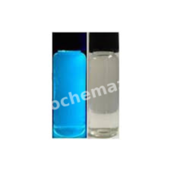
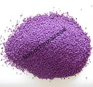
Carbon Quantum Dots (CQD) 565 nm

Price range: $720.00 through $1,290.00
Select options This product has multiple variants. The options may be chosen on the product page
APPLICATIONS Carbon quantum dots are employed in the following because of their optical, electrical, and biological characteristics:
  • Bioimaging,
  • Photovoltaics,
  • Photocatalysis,
  • Drug delivery,
  • Sensors,
  • Optronics.

Tantalum (Ta) Sputtering Targets, Purity: 99.95%, Size: 4”, Thickness: 0.125”

$720.00

Applications of Sputtering Targets;

Film deposition is accomplished using sputtering targets. A technique for sputtering thin films is called "deposition made by sputter targets," which entails eroding material from a "target" source onto a "substrate" like a silicon wafer. Etching of the target is done using semiconductor sputtering targets. When selectivity is not an issue and a high degree of etching anisotropy is required, sputter etching is the method of choice. By removing the target material through etching, sputter targets are also utilized for investigation. In secondary ion spectroscopy (SIMS), one example is when the target material is sputtered at a steady pace. Mass spectrometry is used to quantify the concentration and identity of spewed atoms as the target is sputtered.

The target material's composition may be ascertained and even very low concentrations of contaminants can be found with the aid of the sputtering target.

There is also an application area for sputtering targets in space. One type of space weathering that alters the chemical and physical characteristics of airless worlds like the Moon and asteroids is sputtering.

Cesium chloride(CsCl, 99%) (559836)

$720.00
Select options This product has multiple variants. The options may be chosen on the product page
Cesium chloride(CsCl, 99%) (559836) This product is for research purposes only and is NOT intended for use as drugs, food additives, households, pesticides, etc.
CsCl min% Impurities Max%
Li Na K Rb Ca Mg Fe Al Si Pb
99 0.001 0.02 0.02 0.5 0.005 0.001 0.001 0.001 0.001 0.001


Product Codes- NCZ-2742K

Tungsten Titanium (TiW) Sputtering Targets, Purity: 99.99%, Size: 4”, Thickness: 0.125”

$721.00

Product 

Tungsten Titanium (TiW) Sputtering Targets, Purity: 99.99%, Size: 4'', Thickness: 0.125''

CAS No.

58397-70-9

Appearance

Powder

Purity

≥99%,  ≥99.9%,  ≥95%

(Other purities are also available)

APS

N/A  (Size Can be customized), Ask for other available size ranges.

Ingredient

N/A

Molecular Weight

~231.71 g/mol

Melting Point

~2,700–3,200 °C

Boiling Point

~4,500–5,000 °C

Density

~14.5–17.0 g/cm³

Product Codes

NCZ-1556K

Lanthanum Titanate (LaTiO3) Sputtering Targets, Purity: 99.9%, Size: 2”, Thickness: 0.250”

$723.00

Applications of Sputtering Targets;

  • Sputtering targets is used for film deposition. The deposition made by sputter targets is a method of depositing thin films by sputtering that involves eroding material from a "target" source onto a "substrate" such as  a silicon wafer.
  • Semiconductor sputtering targets is used to etch the target. Sputter etching is chosen in cases where a high degree of etching anisotropy is needed and selectivity is not a concern.
  • Sputter targets is also used for analysis by etching away the target material.
One of the example occurs in secondary ion spectroscopy (SIMS), where the target sample is sputtered at a constant rate. As the target is sputtered, the concentration and identity of sputtered atoms are measured using mass spectrometry. By helping of the sputtering target, the composition of the target material can be determined and even extremely low concentrations of impurities are detected. Sputtering target has also application area in space. Sputtering is one of the forms of space weathering, a process that changes the physical and chemical properties of airless bodies, such as asteroids and the Moon.

Bismuth Ferrite (BiFeO3) Sputtering Targets, Purity: 99.9%, Size: 2”, Thickness: 0.125”

$723.00

Applications of Sputtering Targets;

Film deposition is accomplished using sputtering targets. A technique for sputtering thin films is called "deposition made by sputter targets," which entails eroding material from a "target" source onto a "substrate" like a silicon wafer. Etching of the target is done using semiconductor sputtering targets. When selectivity is not an issue and a high degree of etching anisotropy is required, sputter etching is the method of choice. By removing the target material through etching, sputter targets are also utilized for investigation. In secondary ion spectroscopy (SIMS), one example is when the target material is sputtered at a steady pace. Mass spectrometry is used to quantify the concentration and identity of spewed atoms as the target is sputtered. With the sputtering target's assistance, the

There is also an application area for sputtering targets in space. One type of space weathering that alters the chemical and physical characteristics of airless worlds like the Moon and asteroids is sputtering.

One of the most promising multiferroic materials is bismuth ferrite, an inorganic chemical compound with a perovskite structure and the chemical formula BiFeO3. In order to create a one-phase material called bismuth ferrite (BiFeO3), a bismuth ferrite sputtering target is often manufactured by high temperature sinttering or recrystallizing the mixture of the oxide compound of Bi and Fe. For targets that are sputtering bismuth ferrite, indium bonding is advised.

Titanium Dioxide (TiO2) Sputtering Targets, indium, Purity: 99.9%, Size: 2”, Thickness: 0.125”, Grey to Black

$724.00

Product 

Titanium Dioxide (TiO2) Sputtering Targets, indium, Purity: 99.9%, Size: 2'', Thickness: 0.125'', Grey to Black

CAS No.

13463‑67‑7

Appearance

Powder

Purity

≥99%,  ≥99.9%,  ≥95%

(Other purities are also available)

APS

TiO₂ (black granules) (Size Can be customized), Ask for other available size ranges.

Ingredient

N/A

Molecular Weight

79.94 g/mol

Melting Point

~1,843 °C

Boiling Point

~2,972 °C

Density

~4.23 g/cm³

Product Codes

NCZ-1425K

Niobium Carbide (Nb4C3Tx) MXene Multilayer Nanoflakes, 1g

$725.00
Product Niobium Carbide (Nb4C3Tx) MXene Multilayer Nanoflakes, 1g
CAS No. N/A
Appearance Dark gray
Purity ≥99%,  ≥99.9%,  ≥95%(Other purities are also available)
APS 1–5µm (Size Can be customized),  Ask for other available size range.
Ingredient Nb4C3Tx
Molecular Weight N/A
Melting Point N/A
Boiling Point N/A
Density N/A
Product Codes NCZ-482I

C3N Quantum Dot Powder, 50mg

$726.00
Product C3N Quantum Dot Powder, 50mg
CAS No. N/A
Appearance Black to dark brown
Purity ≥99%,  ≥99.9%,  ≥95%(Other purities are also available)
APS 13–33nm (Size Can be customized),  Ask for other available size range.
Ingredient C3N
Molecular Weight 10.81 g/mol
Melting Point N/A
Boiling Point N/A
Density N/A
Product Codes NCZ-301I

Lithium Nickel Cobalt Oxide (LiNi(1-x)CoxO2) Sputtering Targets, Purity: 99.9%, Size: 2”, Thickness: 0.250”

$726.00

Product 

Lithium Nickel Cobalt Oxide (LiNi(1-x)CoxO2) Sputtering Targets, Purity: 99.9%, Size: 2'', Thickness: 0.250''

CAS No.

113066-89-0 (commonly used for LiNi₀.₈Co₀.₂O₂)

Appearance

Powder

Purity

≥99%,  ≥99.9%,  ≥95%

(Other purities are also available)

APS

 N/A (Size Can be customized), Ask for other available size ranges.

Ingredient

N/A

Molecular Weight

 ~365.38 g/mol (for LiNi₀.₈Co₀.₂O₂)

Melting Point

 >1000 °C (approximate; exact point varies slightly with composition)

Boiling Point

N/A

Density

 ~4.6–4.8 g/cm³ (theoretical)

Product Codes

NCZ-2043K

Barium Fluoride (BaF2) Sputtering Targets, Purity: 99.99%, Size: 2”, Thickness: 0.250”

$727.00

Applications of Sputtering Targets;

Film deposition is accomplished using sputtering targets. A technique for sputtering thin films is called "deposition made by sputter targets," which entails eroding material from a "target" source onto a "substrate" like a silicon wafer. Etching of the target is done using semiconductor sputtering targets. When selectivity is not an issue and a high degree of etching anisotropy is required, sputter etching is the method of choice. By removing the target material through etching, sputter targets are also utilized for investigation. In secondary ion spectroscopy (SIMS), one example is when the target material is sputtered at a steady pace. Mass spectrometry is used to quantify the concentration and identity of spewed atoms as the target is sputtered. With the sputtering target's assistance, the

It is possible to identify the target material and even detect incredibly tiny impurity amounts.

There is also an application area for sputtering targets in space. One type of space weathering that alters the chemical and physical characteristics of airless worlds like the Moon and asteroids is sputtering.

A chemical compound consisting of barium and fluorine, barium fluoride (BaF2) is a salt. It is a solid that has the potential to be a clear crystal. One chemical compound for the 10–20 µm wavelength infrared area is barium fluoride. Enamel, glazing frits, and aluminum metallurgy all use barium fluoride.

Zinc Sulfide (ZnS) Sputtering Targets, Purity: 99.99%, Size: 3”, Thickness: 0.125”

$727.00

Product 

Zinc Sulfide (ZnS) Sputtering Targets, Purity: 99.99%, Size: 3'', Thickness: 0.125''

CAS No.

1314-98-3

Appearance

Powder

Purity

≥99%,  ≥99.9%,  ≥95%

(Other purities are also available)

APS

 (ZnS) (Size Can be customized), Ask for other available size ranges.

Ingredient

N/A

Molecular Weight

97.45 g/mol

Melting Point

~1700 °C

Boiling Point

N/A

Density

 4.09 g/cm³

Product Codes

NCZ-1505K

Silicon Nitride (Si3N4) Sputtering Targets, Purity: 99.5%, Size: 3”, Thickness: 0.250”, Dark Gray to Black

$728.00

Product 

Silicon Nitride (Si3N4) Sputtering Targets, Purity: 99.5%, Size: 3'', Thickness: 0.250'', Dark Gray to Black

CAS No.

 12033-89-5

Appearance

Powder

Purity

≥99%,  ≥99.9%,  ≥95%

(Other purities are also available)

APS

N/A  (Size Can be customized), Ask for other available size ranges.

Ingredient

N/A

Molecular Weight

 140.28 g/mol

Melting Point

 ~1900 °C

Boiling Point

N/A

Density

~3.2 g/cm³

Product Codes

NCZ-1695K

Silicon Carbide (SiC) Sputtering Targets, Purity: 99.5%, Size: 4”, Thickness: 0.250”

$728.00

Product 

Silicon Carbide (SiC) Sputtering Targets, Purity: 99.5%, Size: 4'', Thickness: 0.250''

CAS No.

 409-21-2

Appearance

Powder

Purity

≥99%,  ≥99.9%,  ≥95%

(Other purities are also available)

APS

N/A  (Size Can be customized), Ask for other available size ranges.

Ingredient

N/A

Molecular Weight

 40.10 g/mol

Melting Point

~2,700 °C

Boiling Point

N/A

Density

~3.21 g/cm³

Product Codes

NCZ-1724K

Silicon Carbide (SiC) Sputtering Targets, Purity: 99.5%, Size: 3”, Thickness: 0.250”

$728.00

Product 

Silicon Carbide (SiC) Sputtering Targets, Purity: 99.5%, Size: 3'', Thickness: 0.250''

CAS No.

 409-21-2

Appearance

Powder

Purity

≥99%,  ≥99.9%,  ≥95%

(Other purities are also available)

APS

N/A  (Size Can be customized), Ask for other available size ranges.

Ingredient

N/A

Molecular Weight

 40.10 g/mol

Melting Point

~2,700 °C

Boiling Point

N/A

Density

~3.21 g/cm³

Product Codes

NCZ-1725K

Barium Titanate (BaTiO3) Sputtering Targets, Purity: 99.99%, Size: 3”, Thickness: 0.125”

$728.00

Product 

Barium Titanate (BaTiO3) Sputtering Targets, Purity: 99.99%, Size: 3'', Thickness: 0.125''

CAS No.

 12047‑27‑7

Appearance

Powder

Purity

≥99%,  ≥99.9%,  ≥95%

(Other purities are also available)

APS

1 – 5 µm (Size Can be customized), Ask for other available size ranges.

Ingredient

N/A

Molecular Weight

~233.19 g/mol

Melting Point

~1625 °C

Boiling Point

N/A

Density

 ~6.02 g/cm³

Product Codes

NCZ-2462K

Aluminum Nitride (AlN) Sputtering Targets, Purity: 99.8%, Size: 2”, Thickness: 0.125”

$728.00

Product 

Aluminum Nitride (AlN) Sputtering Targets, Purity: 99.8%, Size: 2'', Thickness: 0.125''

CAS No.

 24304-00-5

Appearance

Powder

Purity

≥99%,  ≥99.9%,  ≥95%

(Other purities are also available)

APS

N/A (Size Can be customized), Ask for other available size ranges.

Ingredient

N/A

Molecular Weight

40.99 g/mol

Melting Point

 ~2200 °C

Boiling Point

 N/A

Density

 ~3.26 g/cm³

Product Codes

NCZ-2559K

Cerium hexaboride(CeB6, 99.9%, 360 mesh) (585927)

$728.00
Select options This product has multiple variants. The options may be chosen on the product page
Cerium hexaboride(CeB6, 99.9%, 360 mesh) (585927)
Product Codes- NCZ-2700K

Yttrium (Y) Sputtering Targets, Purity: 99.9%, Size: 4”, Thickness: 0.125”

$729.00

Applications of Sputtering Targets;

  • Sputtering targets is used for film deposition. The deposition made by sputter targets is a method of depositing thin films by sputtering that involves eroding material from a "target" source onto a "substrate" such as  a silicon wafer.
  • Semiconductor sputtering targets is used to etch the target. Sputter etching is chosen in cases where a high degree of etching anisotropy is needed and selectivity is not a concern.
  • Sputter targets is also used for analysis by etching away the target material.
One of the example occurs in secondary ion spectroscopy (SIMS), where the target sample is sputtered at a constant rate. As the target is sputtered, the concentration and identity of sputtered atoms are measured using mass spectrometry. By helping of the sputtering target, the composition of the target material can be determined and even extremely low concentrations of impurities are detected. Sputtering target has also application area in space. Sputtering is one of the forms of space weathering, a process that changes the physical and chemical properties of airless bodies, such as asteroids and the Moon.

Magnesium Oxide (MgO) Sputtering Targets, Purity: 99.95%, Size: 2”, Thickness: 0.125”

$730.00

Applications of Sputtering Targets;

Film deposition is accomplished using sputtering targets. A technique for sputtering thin films is called "deposition made by sputter targets," which entails eroding material from a "target" source onto a "substrate" like a silicon wafer. Etching of the target is done using semiconductor sputtering targets. When selectivity is not an issue and a high degree of etching anisotropy is required, sputter etching is the method of choice. By removing the target material through etching, sputter targets are also utilized for investigation. In secondary ion spectroscopy (SIMS), one example is when the target material is sputtered at a steady pace. Mass spectrometry is used to quantify the concentration and identity of spewed atoms as the target is sputtered.

By helping of the sputtering target, the composition of the target material may be evaluated and even extremely tiny amounts of contaminants are recognized.

There is also an application area for sputtering targets in space. One type of space weathering that alters the chemical and physical characteristics of airless worlds like the Moon and asteroids is sputtering.

Molybdenum Disulfide (MoS2) Sputtering Targets, indium, Purity: 99.9%, Size: 2”, Thickness: 0.125”

$730.00

Applications of Sputtering Targets;

Film deposition is accomplished using sputtering targets. A technique for sputtering thin films is called "deposition made by sputter targets," which entails eroding material from a "target" source onto a "substrate" like a silicon wafer. Etching of the target is done using semiconductor sputtering targets. When selectivity is not an issue and a high degree of etching anisotropy is required, sputter etching is the method of choice. By removing the target material through etching, sputter targets are also utilized for investigation. In secondary ion spectroscopy (SIMS), one example is when the target material is sputtered at a steady pace. Mass spectrometry is used to quantify the concentration and identity of spewed atoms as the target is sputtered.

By helping of the sputtering target, the composition of the target material may be evaluated and even extremely tiny amounts of contaminants are recognized.

There is also an application area for sputtering targets in space. One type of space weathering that alters the chemical and physical characteristics of airless worlds like the Moon and asteroids is sputtering.

Molybdenum Disulfide (MoS2) Sputtering Targets, Purity: 99.9%, Size: 3”, Thickness: 0.250”

$730.00

Product 

Molybdenum Disulfide (MoS2) Sputtering Targets, Purity: 99.9%, Size: 3'', Thickness: 0.250''

CAS No.

 1317-33-5

Appearance

Powder

Purity

≥99%,  ≥99.9%,  ≥95%

(Other purities are also available)

APS

 N/A (Size Can be customized), Ask for other available size ranges.

Ingredient

N/A

Molecular Weight

 160.07 g/mol

Melting Point

 ~1185 °C

Boiling Point

 ~4500 °C

Density

 ~5.06 g/cm³

Product Codes

NCZ-1914K

Molybdenum Disilicide (MoSi2) Sputtering Targets, Purity: 99.95%, Size: 3”, Thickness: 0.250”

$730.00

Product 

Molybdenum Disilicide (MoSi2) Sputtering Targets, Purity: 99.95%, Size: 3'', Thickness: 0.250''

CAS No.

12136-78-6

Appearance

Powder

Purity

≥99%,  ≥99.9%,  ≥95%

(Other purities are also available)

APS

 N/A (Size Can be customized), Ask for other available size ranges.

Ingredient

N/A

Molecular Weight

152.11 g/mol

Melting Point

 ~2030 °C

Boiling Point

 ~2300 °C to 2500 °C

Density

~6.26 g/cm³

Product Codes

NCZ-1924K

Boron (B) Sputtering Targets, indium, Purity: 99.9%, Size: 3”, Thickness: 0.125”

$732.00

Applications of Sputtering Targets;

Film deposition is accomplished using sputtering targets. A technique for sputtering thin films is called "deposition made by sputter targets," which entails eroding material from a "target" source onto a "substrate" like a silicon wafer. Etching of the target is done using semiconductor sputtering targets. When selectivity is not an issue and a high degree of etching anisotropy is required, sputter etching is the method of choice. By removing the target material through etching, sputter targets are also utilized for investigation. In secondary ion spectroscopy (SIMS), one example is when the target material is sputtered at a steady pace. Mass spectrometry is used to quantify the concentration and identity of spewed atoms as the target is sputtered.

The target material's composition may be ascertained and even very low concentrations of contaminants can be found with the aid of the sputtering target.

There is also an application area for sputtering targets in space. One type of space weathering that alters the chemical and physical characteristics of airless worlds like the Moon and asteroids is sputtering.

Tantalum (Ta) Sputtering Targets, Purity: 99.95%, Size: 4”, Thickness: 0.250”

$732.00

Applications of Sputtering Targets;

Film deposition is accomplished using sputtering targets. A technique for sputtering thin films is called "deposition made by sputter targets," which entails eroding material from a "target" source onto a "substrate" like a silicon wafer. Etching of the target is done using semiconductor sputtering targets. When selectivity is not an issue and a high degree of etching anisotropy is required, sputter etching is the method of choice. By removing the target material through etching, sputter targets are also utilized for investigation. In secondary ion spectroscopy (SIMS), one example is when the target material is sputtered at a steady pace. Mass spectrometry is used to quantify the concentration and identity of spewed atoms as the target is sputtered.

The target material's composition may be ascertained and even very low concentrations of contaminants can be found with the aid of the sputtering target.

There is also an application area for sputtering targets in space. One type of space weathering that alters the chemical and physical characteristics of airless worlds like the Moon and asteroids is sputtering.

Zinc Oxide (ZnO) with Alumina Sputtering Targets, Purity: 99.99%, Size: 4”, Thickness: 0.250”

$732.00

Product 

Zinc Oxide (ZnO) with Alumina Sputtering Targets, Purity: 99.99%, Size: 4'', Thickness: 0.250''

CAS No.

ZnO: 1314-13-2 Al₂O₃: 1344-28-1

Appearance

Powder

Purity

≥99%,  ≥99.9%,  ≥95%

(Other purities are also available)

APS

ZnO + Al₂O₃ (AZO)(black granules) (Size Can be customized), Ask for other available size ranges.

Ingredient

N/A

Molecular Weight

ZnO: 81.38 g/mol Al₂O₃: 101.96 g/mol

Melting Point

~1975 °C

Boiling Point

N/A

Density

~5.6 g/cm³

Product Codes

NCZ-1485K

Aluminum Oxide (Al2O3) Sputtering Targets, Purity: 99.999%, Size: 3”, Thickness: 0.125”

$732.00

Product 

Aluminum Oxide (Al2O3) Sputtering Targets, Purity: 99.999%, Size: 3'', Thickness: 0.125''

CAS No.

 1344-28-1

Appearance

Powder

Purity

≥99%,  ≥99.9%,  ≥95%

(Other purities are also available)

APS

N/A (Size Can be customized), Ask for other available size ranges.

Ingredient

N/A

Molecular Weight

101.96 g/mol

Melting Point

~2,072 °C

Boiling Point

~2,977 °C

Density

~3.97–3.98 g/cm³

Product Codes

NCZ-2540K

4N 99.99% Tantalum Disulfide (TaS2) Powder

Price range: $733.00 through $2,053.00
Select options This product has multiple variants. The options may be chosen on the product page
Product 4N 99.99% Tantalum Disulfide (TaS2) Powder
CAS No. 12143-72-5
Appearance Dark brown
Purity ≥99%,  ≥99.9%,  ≥95%(Other purities are also available)
APS N/A
Ingredient TaS2
Molecular Weight 245.07 g/mol
Melting Point N/A
Boiling Point N/A
Density 6.86 g/cm³
Product Codes NCZ-180I

4N 99.99% Zirconium Disulfide (ZrS2) Powder

Price range: $733.00 through $1,283.00
Select options This product has multiple variants. The options may be chosen on the product page
Product 4N 99.99% Zirconium Disulfide (ZrS2) Powder
CAS No. 12039-15-5
Appearance Red Brown
Purity ≥99%,  ≥99.9%,  ≥95%(Other purities are also available)
APS N/A
Ingredient ZrS2
Molecular Weight 155.35 g/mol
Melting Point 1,480 °C
Boiling Point N/A
Density N/A
Product Codes NCZ-181I
 

Indium Zinc Oxide/IZO (InZnO) Sputtering Targets, indium, Purity: 99.99%, Size: 2”, Thickness: 0.125”

$734.00

Product 

Indium Zinc Oxide/IZO (InZnO) Sputtering Targets, indium, Purity: 99.99%, Size: 2'', Thickness: 0.125''

CAS No.

Indium oxide (In₂O₃): 1312-43-2
Zinc oxide (ZnO): 1314-13-2

Appearance

Powder

Purity

≥99%,  ≥99.9%,  ≥95%

(Other purities are also available)

APS

 N/A (Size Can be customized), Ask for other available size ranges.

Ingredient

N/A

Molecular Weight

90% In₂O₃ (277.64 g/mol), 10% ZnO (81.38 g/mol) → ~260–270 g/mol (estimated)

Melting Point

Indium oxide: ~1910 °C Zinc oxide: ~1975 °C

Boiling Point

N/A

Density

~7.1 g/cm³

Product Codes

NCZ-2194K

Poly(Lactide-co-trimethylene carbonate)(PLTMC75/25) (613989)

$734.00
Poly(Lactide-co-trimethylene carbonate)(PLTMC75/25) (613989)
Grade Description Inherent viscosity (dL/g) Weight average molecular weight (x10000)
PLTMC75-10 PLTMC75/25 0.5-1.0 5-12
PLTMC75-15 PLTMC75/25 1.0-1.5 12-20
PLTMC75-20 PLTMC75/25 1.5-2.0 20-30
Product Codes- NCZ-2648K

Carbon Quantum Dots (CQD) 535 nm

Price range: $735.00 through $1,310.00
Select options This product has multiple variants. The options may be chosen on the product page
APPLICATIONS Carbon quantum dots are employed in the following because of their optical, electrical, and biological characteristics:
  • Bioimaging,
  • Photovoltaics,
  • Photocatalysis,
  • Drug delivery,
  • Sensors,
  • Optronics.

Barium (Ba) Sputtering Targets, Purity: 99.5%, Size: 4”, Thickness: 0.250”

$735.00

Applications of Sputtering Targets;

Film deposition is accomplished using sputtering targets. A technique for sputtering thin films is called "deposition made by sputter targets," which entails eroding material from a "target" source onto a "substrate" like a silicon wafer. Etching of the target is done using semiconductor sputtering targets. When selectivity is not an issue and a high degree of etching anisotropy is required, sputter etching is the method of choice. By removing the target material through etching, sputter targets are also utilized for investigation. In secondary ion spectroscopy (SIMS), one example is when the target material is sputtered at a steady pace. When the target shatters,

Mass spectrometry measures the concentration and identity of sputtered atoms. The target material's composition may be ascertained and even very low concentrations of contaminants can be found with the aid of the sputtering target.

There is also an application area for sputtering targets in space. One type of space weathering that alters the chemical and physical characteristics of airless worlds like the Moon and asteroids is sputtering.

A Block S, Group 2, Period 6 element with an atomic weight of 137.27, barium has the atomic symbol Ba and atomic number 56. Barium is a mineral that  an alkaline-earth metal member. Electronics can be plated using barium sputtering targets. Barium is beneficial for sputtering applications because of its good electrical characteristics. Barium sputtering targets can be utilized for semiconductors. Barium sputtering targets will work well for flat panel displays. Barium can be combined with other metals, such as titanium and strontium, to create alloys with more specialized qualities.

Barium (Ba) Sputtering Targets, Purity: 99.5%, Size: 4”, Thickness: 0.125”

$735.00

Applications of Sputtering Targets;

Film deposition is accomplished using sputtering targets. A technique for sputtering thin films is called "deposition made by sputter targets," which entails eroding material from a "target" source onto a "substrate" like a silicon wafer. Etching of the target is done using semiconductor sputtering targets. When selectivity is not an issue and a high degree of etching anisotropy is required, sputter etching is the method of choice. By removing the target material through etching, sputter targets are also utilized for investigation. In secondary ion spectroscopy (SIMS), one example is when the target material is sputtered at a steady pace. Mass spectrometry is used to quantify the concentration and identity of spewed atoms as the target is sputtered. With the sputtering target's assistance, the

It is possible to identify the target material and even detect incredibly tiny impurity amounts.

There is also an application area for sputtering targets in space. One type of space weathering that alters the chemical and physical characteristics of airless worlds like the Moon and asteroids is sputtering.

A Block S, Group 2, Period 6 element with an atomic weight of 137.27, barium has the atomic symbol Ba and atomic number 56. One of the alkaline-earth metals is barium. Electronics can be plated using barium sputtering targets. Barium is beneficial for sputtering applications because of its good electrical characteristics. Barium sputtering targets can be utilized for semiconductors. Barium for flat panel screens

Tungsten Oxide (WO3) Sputtering Targets, Purity: 99.9%, Size: 1”, Thickness: 0.125”

$735.00

Applications of Sputtering Targets;

Film deposition is accomplished using sputtering targets. A technique for sputtering thin films is called "deposition made by sputter targets," which entails eroding material from a "target" source onto a "substrate" like a silicon wafer. Etching of the target is done using semiconductor sputtering targets. When selectivity is not an issue and a high degree of etching anisotropy is required, sputter etching is the method of choice. By removing the target material through etching, sputter targets are also utilized for investigation. In secondary ion spectroscopy (SIMS), one example is when the target material is sputtered at a steady pace. Mass spectrometry is used to quantify the concentration and identity of spewed atoms as the target is sputtered.

The target material's composition may be ascertained and even very low concentrations of contaminants can be found with the aid of the sputtering target.

There is also an application area for sputtering targets in space. One type of space weathering that alters the chemical and physical characteristics of airless worlds like the Moon and asteroids is sputtering.

Boron Carbide (B4C) Sputtering Targets, indium, Purity: 99.5%, Size: 2”, Thickness: 0.125”

$735.00

Product 

Boron Carbide (B4C) Sputtering Targets, indium, Purity: 99.5%, Size: 2'', Thickness: 0.125''

CAS No.

12069‑32‑8

Appearance

Powder

Purity

≥99%,  ≥99.9%,  ≥95%

(Other purities are also available)

APS

 N/A (Size Can be customized), Ask for other available size ranges.

Ingredient

N/A

Molecular Weight

 ~55.26 g/mol

Melting Point

~2350 °C

Boiling Point

> 3500 °C (decomposes above ~2800 °C)

Density

 ~2.37 g/cm³ (theoretical)

Product Codes

NCZ-2378K

Indium (In) Sputtering Targets, Purity: 99.999%, Size: 3”, Thickness: 0.250”

$736.00

Product 

Indium (In) Sputtering Targets, Purity: 99.999%, Size: 3'', Thickness: 0.250''

CAS No.

 7440-74-6

Appearance

Powder

Purity

≥99%,  ≥99.9%,  ≥95%

(Other purities are also available)

APS

 N/A (Size Can be customized), Ask for other available size ranges.

Ingredient

N/A

Molecular Weight

114.82 g/mol

Melting Point

 156.6 °C

Boiling Point

 2,072 °C

Density

 7.31 g/cm³

Product Codes

NCZ-2224K

Praseodymium Fluoride (PrF3) 99% 2N

$737.00
Select options This product has multiple variants. The options may be chosen on the product page
Product Praseodymium Fluoride (PrF3) 99% 2N
CAS No. 13709-46-1
Appearance Pale green crystalline
Purity ≥99%,  ≥99.9%,  ≥95%(Other purities are also available)
APS 1–10µm (Size Can be customized),  Ask for other available size range.
Ingredient PrF3
Molecular Weight 209.90 g/mol
Melting Point N/A
Boiling Point N/A
Density 6.55 g/cm³
Product Codes NCZ-502I

Boron (B) Sputtering Targets, Purity: 99.9%, Size: 4”, Thickness: 0.125”

$738.00

Product 

Boron (B) Sputtering Targets, Purity: 99.9%, Size: 4'', Thickness: 0.125''

CAS No.

7440-42-8

Appearance

Powder

Purity

≥99%,  ≥99.9%,  ≥95%

(Other purities are also available)

APS

 N/A (Size Can be customized), Ask for other available size ranges.

Ingredient

N/A

Molecular Weight

 10.81 g/mol

Melting Point

~2076 °C

Boiling Point

 ~3927 °C

Density

 ~2.34 g/cm³

Product Codes

NCZ-2391K

Tungsten (W) Sputtering Targets, elastomer, Purity: 99.95%, Size: 3”, Thickness: 0.125”

$739.00

Product 

Tungsten (W) Sputtering Targets, elastomer, Purity: 99.95%, Size: 3'', Thickness: 0.125''

CAS No.

 7440-33-7

Appearance

Powder

Purity

≥99%,  ≥99.9%,  ≥95%

(Other purities are also available)

APS

N/A  (Size Can be customized), Ask for other available size ranges.

Ingredient

N/A

Molecular Weight

 183.84 g/mol

Melting Point

3,410 °C

Boiling Point

5,900 °C

Density

19.25 g/cm³

Product Codes

NCZ-1583K

Gallium Oxide (Beta Ga2O3) Powder, 99.999% (5N) (Metal Basis), High Purity

$739.00
Select options This product has multiple variants. The options may be chosen on the product page
Product Gallium Oxide (Beta Ga2O3) Powder, 99.999% (5N) (Metal Basis), High Purity
CAS No. 12024-21-4
Appearance White
Purity ≥99%,  ≥99.9%,  ≥95%(Other purities are also available)
APS N/A
Ingredient Ga2O3
Molecular Weight 187.44 g/mol
Melting Point N/A
Boiling Point N/A
Density 5.88 g/cm³
Product Codes NCZ-352I
 

Indium Oxide (In2O3) Sputtering Targets, Purity: 99.99%, Size: 3”, Thickness: 0.125”

$740.00

Applications of Sputtering Targets;

Film deposition is accomplished using sputtering targets. A technique for sputtering thin films is called "deposition made by sputter targets," which entails eroding material from a "target" source onto a "substrate" like a silicon wafer. Etching of the target is done using semiconductor sputtering targets. When selectivity is not an issue and a high degree of etching anisotropy is required, sputter etching is the method of choice. By removing the target material through etching, sputter targets are also utilized for investigation. In secondary ion spectroscopy (SIMS), one example is when the target material is sputtered at a steady pace. Mass spectrometry is used to quantify the concentration and identity of spewed atoms as the target is sputtered.

The target material's composition may be ascertained and even very low concentrations of contaminants can be found with the aid of the sputtering target.

There is also an application area for sputtering targets in space. One type of space weathering that alters the chemical and physical characteristics of airless worlds like the Moon and asteroids is sputtering.

Tantalum Oxide (Ta2O5) Sputtering Targets, Purity: 99.99%, Size: 3”, Thickness: 0.250”

$740.00

Applications of Sputtering Targets;

Film deposition is accomplished using sputtering targets. A technique for sputtering thin films is called "deposition made by sputter targets," which entails eroding material from a "target" source onto a "substrate" like a silicon wafer. Etching of the target is done using semiconductor sputtering targets. When selectivity is not an issue and a high degree of etching anisotropy is required, sputter etching is the method of choice. By removing the target material through etching, sputter targets are also utilized for investigation. In secondary ion spectroscopy (SIMS), one example is when the target material is sputtered at a steady pace. Mass spectrometry is used to quantify the concentration and identity of spewed atoms as the target is sputtered.

The target material's composition may be ascertained and even very low concentrations of contaminants can be found with the aid of the sputtering target.

There is also an application area for sputtering targets in space. One type of space weathering that alters the chemical and physical characteristics of airless worlds like the Moon and asteroids is sputtering.

Hydroxyapatite Microsphere(Ca10(PO4)6(OH)2, Spherical, 15-60um, D50=35um, Medical grade) (827982)

$740.00
Select options This product has multiple variants. The options may be chosen on the product page

Product 

Hydroxyapatite Microsphere(Ca10(PO4)6(OH)2, Spherical, 15-60um, D50=35um, Medical grade) (827982)

CAS No.

1306‑06‑5

Appearance

Powder

Purity

≥99%,  ≥99.9%,  ≥95%

(Other purities are also available)

APS

 <15 µm (Size Can be customized), Ask for other available size ranges.

Ingredient

N/A

Molecular Weight

 ~1004.7 g/mol

Melting Point

~1650–1670 °C

Boiling Point

N/A

Density

 ~3.16 g/cm³

Product Codes

NCZ-2604K

Iron Oxide (Fe3O4) Sputtering Targets, indium, Purity: 99.9%, Size: 1”, Thickness: 0.125”

$741.00

Applications of Sputtering Targets;

Film deposition is accomplished using sputtering targets. A technique for sputtering thin films is called "deposition made by sputter targets," which entails eroding material from a "target" source onto a "substrate" like a silicon wafer. Etching of the target is done using semiconductor sputtering targets. When selectivity is not an issue and a high degree of etching anisotropy is required, sputter etching is the method of choice. By removing the target material through etching, sputter targets are also utilized for investigation. In secondary ion spectroscopy (SIMS), one example is when the target material is sputtered at a steady pace. Mass spectrometry is used to quantify the concentration and identity of spewed atoms as the target is sputtered.

The target material's composition may be ascertained and even very low concentrations of contaminants can be found with the aid of the sputtering target.

There is also an application area for sputtering targets in space. One type of space weathering that alters the chemical and physical characteristics of airless worlds like the Moon and asteroids is sputtering.

Lanthanum Aluminate Sputtering Target LaAlO3

$741.00
Product Lanthanum Aluminate Sputtering Target LaAlO3
CAS No. 12003-65-5
Appearance Dense, dark-colored ceramic material
Purity ≥99%,  ≥99.9%,  ≥95%(Other purities are also available)
APS N/A
Ingredient LaAlO3
Molecular Weight 213.89 g/mol
Melting Point N/A
Boiling Point N/A
Density 6.52 g/cm3
Product Codes NCZ-124H

Manganese (Mn) Sputtering Targets, indium, Purity: 99.95%, Size: 2”, Thickness: 0.125”

$742.00

Product 

Manganese (Mn) Sputtering Targets, indium, Purity: 99.95%, Size: 2'', Thickness: 0.125''

CAS No.

 7439-96-5

Appearance

Powder

Purity

≥99%,  ≥99.9%,  ≥95%

(Other purities are also available)

APS

 N/A (Size Can be customized), Ask for other available size ranges.

Ingredient

N/A

Molecular Weight

54.94 g/mol

Melting Point

 1,246 °C

Boiling Point

 2,061 °C

Density

 7.21 g/cm³

Product Codes

NCZ-1943K

Aluminum Nitride (AlN) Sputtering Targets, Purity: 99.8%, Size: 3”, Thickness: 0.125”

$744.00

Applications of Sputtering Targets;

  • Sputtering targets is used for film deposition. The deposition made by sputter targets is a method of depositing thin films by sputtering that involves eroding material from a "target" source onto a "substrate" such as  a silicon wafer.
  • Semiconductor sputtering targets is used to etch the target. Sputter etching is chosen in cases where a high degree of etching anisotropy is needed and selectivity is not a concern.
  • Sputter targets is also used for analysis by etching away the target material.
One of the example occurs in secondary ion spectroscopy (SIMS), where the target sample is sputtered at a constant rate. As the target is sputtered, the concentration and identity of sputtered atoms are measured using mass spectrometry. By helping of the sputtering target, the composition of the target material can be determined and even extremely low concentrations of impurities are detected. Sputtering target has also application area in space. Sputtering is one of the forms of space weathering, a process that changes the physical and chemical properties of airless bodies, such as asteroids and the Moon. Aluminum nitride is a chemical compound with the formula of AlN.Aluminum nitride has excellent combination of physical, chemical, and mechanical properties. High-quality films of aluminum nitride have been used in various devices and sensors including the optical and optoelectronic devices. As far as the optical and optoelectronic applications are concerned, wide band gap (~6.2 eV) along with high-refractive index (~2.0) and low-absorption coefficient (<10−3) makes AlN a very attractive material for these applications. In addition to this, thermal and chemical stability of AlN films make it suitable for applications in difficult environment. Today, AlN films/coatings have been grown by several methods which include pulsed laser deposition, reactive molecular beam epitaxy, vacuum arc/cathodic arc deposition, DC/RF reactive sputtering, ion beam sputtering, metal-organic chemical vapor deposition (MOCVD), and miscellaneous other techniques. Due to simplicity, reproducibility, ease of scaling up, and lower cost, magnetron sputtering is one of the common methods for growing AlN films for various applications. Properties of AlN films depend upon the crystal structure, crystal orientation, microstructure, and chemical composition, which in turn depend upon the deposition conditions such as sputtering power, pulse frequency, duty cycle, growth temperature, nitrogen/argon flow ratio, and sputtering gas pressure. AlN sputtering targets give good result with the method of reactive DC magnetron sputtering system.

Aluminum Nitride (AlN) Sputtering Targets, Purity: 99.8%, Size: 3”, Thickness: 0.125”

$744.00

 Applications of Sputtering Targets;

Film deposition is accomplished using sputtering targets. A technique for sputtering thin films is called "deposition made by sputter targets," which entails eroding material from a "target" source onto a "substrate" like a silicon wafer. Etching of the target is done using semiconductor sputtering targets. When selectivity is not an issue and a high degree of etching anisotropy is required, sputter etching is the method of choice. By removing the target material through etching, sputter targets are also utilized for investigation. In secondary ion spectroscopy (SIMS), one example is when the target material is sputtered at a steady pace. When the target shatters,

It is possible to identify the target material and even detect incredibly tiny impurity amounts.

There is also an application area for sputtering targets in space. One type of space weathering that alters the chemical and physical characteristics of airless worlds like the Moon and asteroids is sputtering.

The chemical compound aluminum nitride has the formula AlN. The combination of mechanical, chemical, and physical properties of aluminum nitride is exceptional. Superior aluminum nitride films have found application in a wide range of sensors and devices, including optoelectronic and optical ones. Regarding the optical and optoelectronic uses, a large band gap (~6.2 eV), a high refractive index (~2.0), and low absorption

Titanium Boride (TiB2) Sputtering Targets, Purity: 99.5%, Size: 4”, Thickness: 0.250”

$744.00

Applications of Sputtering Targets;

Film deposition is accomplished using sputtering targets. A technique for sputtering thin films is called "deposition made by sputter targets," which entails eroding material from a "target" source onto a "substrate" like a silicon wafer. Etching of the target is done using semiconductor sputtering targets. When selectivity is not an issue and a high degree of etching anisotropy is required, sputter etching is the method of choice. By removing the target material through etching, sputter targets are also utilized for investigation. In secondary ion spectroscopy (SIMS), one example is when the target material is sputtered at a steady pace. Mass spectrometry is used to quantify the concentration and identity of spewed atoms as the target is sputtered.

The target material's composition may be ascertained and even very low concentrations of contaminants can be found with the aid of the sputtering target.

There is also an application area for sputtering targets in space. One type of space weathering that alters the chemical and physical characteristics of airless worlds like the Moon and asteroids is sputtering.

Calcium Manganate (CaMnO3) Sputtering Targets, Purity: 99.9%, Size: 2”, Thickness: 0.250”

$744.00

Product 

Calcium Manganate (CaMnO3) Sputtering Targets, Purity: 99.9%, Size: 2'', Thickness: 0.250''

CAS No.

12058-85-6

Appearance

Powder

Purity

≥99%,  ≥99.9%,  ≥95%

(Other purities are also available)

APS

 N/A (Size Can be customized), Ask for other available size ranges.

Ingredient

N/A

Molecular Weight

157.87 g/mol

Melting Point

 Approx. 1400 °C (decomposes)

Boiling Point

N/A

Density

 ~4.7 g/cm³

Product Codes

NCZ-2360K

Magnesium Oxide (MgO) Sputtering Targets, Purity: 99.95%, Size: 6”, Thickness: 0.250”

$745.00

Applications of Sputtering Targets;

Film deposition is accomplished using sputtering targets. A technique for sputtering thin films is called "deposition made by sputter targets," which entails eroding material from a "target" source onto a "substrate" like a silicon wafer. Etching of the target is done using semiconductor sputtering targets. When selectivity is not an issue and a high degree of etching anisotropy is required, sputter etching is the method of choice. By removing the target material through etching, sputter targets are also utilized for investigation. In secondary ion spectroscopy (SIMS), one example is when the target material is sputtered at a steady pace. Mass spectrometry is used to quantify the concentration and identity of spewed atoms as the target is sputtered.

By helping of the sputtering target, the composition of the target material may be evaluated and even extremely tiny amounts of contaminants are recognized.

There is also an application area for sputtering targets in space. One type of space weathering that alters the chemical and physical characteristics of airless worlds like the Moon and asteroids is sputtering.

Molybdenum Disulfide (MoS2) Sputtering Targets, Purity: 99.9%, Size: 6”, Thickness: 0.250”

$745.00

Applications of Sputtering Targets;

Film deposition is accomplished using sputtering targets. A technique for sputtering thin films is called "deposition made by sputter targets," which entails eroding material from a "target" source onto a "substrate" like a silicon wafer. Etching of the target is done using semiconductor sputtering targets. When selectivity is not an issue and a high degree of etching anisotropy is required, sputter etching is the method of choice. By removing the target material through etching, sputter targets are also utilized for investigation. In secondary ion spectroscopy (SIMS), one example is when the target material is sputtered at a steady pace. Mass spectrometry is used to quantify the concentration and identity of spewed atoms as the target is sputtered.

The target material's composition may be ascertained and even very low concentrations of contaminants can be found with the aid of the sputtering target.

There is also an application area for sputtering targets in space. One type of space weathering that alters the chemical and physical characteristics of airless worlds like the Moon and asteroids is sputtering.

Antimony Tin Oxide Nanoparticles/ Nanopowder Dispersion in aromatic

$745.00
Select options This product has multiple variants. The options may be chosen on the product page
$745/500g

Product 

Antimony Tin Oxide Nanoparticles/ Nanopowder Dispersion in aromatic

CAS No.

1332-09-8

Appearance

Powder

Purity

≥99%,  ≥99.9%,  ≥95%

(Other purities are also available)

APS

<20nm (Size Can be customized), Ask for other available size ranges.

Ingredient

N/A

Molecular Weight

~150–170 g/mol

Melting Point

~1,100 – 1,300 °C

Boiling Point

N/A

Density

~6.5–7.2 g/cm³

Product Codes

NCZ-1183K

Antimony Tin Oxide Nanoparticles/ Nanopowder Dispersion in Alcohols (Copy)

$745.00
Select options This product has multiple variants. The options may be chosen on the product page
$745/500g

Product 

Antimony Tin Oxide Nanoparticles/ Nanopowder Dispersion in Alcohols

CAS No.

1332-09-8

Appearance

Powder

Purity

≥99%,  ≥99.9%,  ≥95%

(Other purities are also available)

APS

<20nm (Size Can be customized), Ask for other available size ranges.

Ingredient

N/A

Molecular Weight

160–165 g/mol

Melting Point

~1,100 – 1,300 °C

Boiling Point

N/A

Density

~6.5–7.2 g/cm³

Product Codes

NCZ-1185K

Doped Tin Oxide Nanoparticles/ Nanopowder Dispersion in Aromatic(DTO)

$745.00
Select options This product has multiple variants. The options may be chosen on the product page
$745/500g

Product 

Doped Tin Oxide Nanoparticles/ Nanopowder Dispersion in Aromatic(DTO)

CAS No.

18282-10-5

Appearance

Powder

Purity

≥99%,  ≥99.9%,  ≥95%

(Other purities are also available)

APS

10~15nm (Size Can be customized), Ask for other available size ranges.

Ingredient

N/A

Molecular Weight

~150–165 g/mol

Melting Point

~1630 °C

Boiling Point

N/A

Density

 6.9–7.1 g/cm³

Product Codes

NCZ-1186K

Doped Tin Oxide Nanoparticles/ Nanopowder Dispersion in Alcohols(DTO)

$745.00
Select options This product has multiple variants. The options may be chosen on the product page
$745/500g

Product 

Doped Tin Oxide Nanoparticles/ Nanopowder Dispersion in Alcohols(DTO)

CAS No.

18282-10-5

Appearance

Powder

Purity

≥99%,  ≥99.9%,  ≥95%

(Other purities are also available)

APS

10–15 nm (Size Can be customized), Ask for other available size ranges.

Ingredient

N/A

Molecular Weight

~150–165 g/mol

Melting Point

~1630 °C

Boiling Point

N/A

Density

 6.9–7.1 g/cm³

Product Codes

NCZ-1187K

Doped Tin Oxide Nanoparticles/ Nanopowder Dispersion in Water(DTO)

$745.00
Select options This product has multiple variants. The options may be chosen on the product page
$745/500g

Product 

Doped Tin Oxide Nanoparticles/ Nanopowder Dispersion in Water(DTO)

CAS No.

18282-10-5

Appearance

Powder

Purity

≥99%,  ≥99.9%,  ≥95%

(Other purities are also available)

APS

10~15nm (Size Can be customized), Ask for other available size ranges.

Ingredient

N/A

Molecular Weight

~150–165 g/mol

Melting Point

~1630 °C

Boiling Point

N/A

Density

 6.9–7.1 g/cm³

Product Codes

NCZ-1190K

Tungsten Titanium (TiW) Sputtering Targets, Purity: 99.99%, Size: 3”, Thickness: 0.250”

$745.00

Product 

Tungsten Titanium (TiW) Sputtering Targets, Purity: 99.99%, Size: 3'', Thickness: 0.250''

CAS No.

58397-70-9

Appearance

Powder

Purity

≥99%,  ≥99.9%,  ≥95%

(Other purities are also available)

APS

N/A  (Size Can be customized), Ask for other available size ranges.

Ingredient

N/A

Molecular Weight

~231.71 g/mol

Melting Point

~2,700–3,200 °C

Boiling Point

~4,500–5,000 °C

Density

~14.5–17.0 g/cm³

Product Codes

NCZ-1557K

Kish Graphite(industrial grade, 80-90%) (371667)

$745.00
Select options This product has multiple variants. The options may be chosen on the product page
Kish Graphite(industrial grade, 80-90%) (371667)
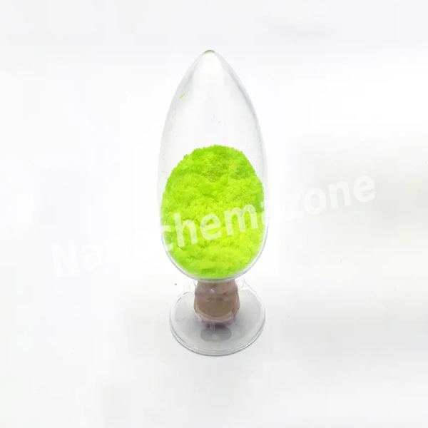
  Kish Graphite is a byproduct of steel-making. The more modern steel-making processes do not result in the generation of Kish graphite, but in earlier times it was produced during the cooling of molten steel. It is obtained when carbon crystallizes from molten steel during the steel manufacturing process. It is used by hundreds of research groups to make graphene by mechanical exfoliation.  With preparation methods, the size of kish graphite is from mm to cm. As it is obtained by high temperature, the main applications include: as raw materials to synthesis the graphene, graphite intercalation compounds, and the fundamental research works such as the properties of graphite, large size graphite layer compounds.
Product Codes- NCZ-2717K