Samarium Oxide Nanopowder/ Nanoparticles (Sm2O3, 99.9%, 100nm)

$215.00
Select options This product has multiple variants. The options may be chosen on the product page
$215/25g
Product Samarium Oxide Nanopowder/ Nanoparticles (Sm2O3, 99.9%, 100nm)
CAS No. 12060-58-1
Appearance Yellow to white powder
Purity ≥99%,  ≥99.9%,  ≥95%(Other purities are also available)
APS 100nm (Size Can be customized),  Ask for other available size range.
Ingredient Sm₂O₃. 
Molecular Weight 348.72 g/mol
Melting Point 2,335° C
Boiling Point 4,118° C
Density 8.347g/cm3
Product Codes NCZ-120R
 

Samarium TMHD

Price range: $39.00 through $222.00
Select options This product has multiple variants. The options may be chosen on the product page
Product Samarium TMHD
CAS No. 15492-50-9
Appearance Pale yellow crystalline
Purity ≥99%,  ≥99.9%,  ≥95%(Other purities are also available)
APS N/A
Ingredient C₃₃H₅₇O₆Sm
Molecular Weight N/A
Melting Point 191–193 °C
Boiling Point 250 °C
Density N/A
Product Codes NCZ-361R
 

Samarium TTFA

Price range: $28.00 through $169.00
Select options This product has multiple variants. The options may be chosen on the product page
Product Samarium TTFA
CAS No. N/A
Appearance Pale yellow to orange solid
Purity ≥99%,  ≥99.9%,  ≥95%(Other purities are also available)
APS N/A
Ingredient C₂₇H₁₅F₉O₆S₃Sm
Molecular Weight 810.5 g/mol
Melting Point N/A
Boiling Point N/A
Density N/A
Product Codes NCZ-398R

SAPO-11 (972853)

$290.00
SAPO-11 (972853)

Pore Structure AEL Pore Size(nm) 0.6 - 0.7 SiO2/P2O5/Al2O3 = 0-0.3 : 1 : 1, 0.3-0.5 : 1 : 1, 0.5-0.8 : 1 : 1 Relative Crystallinity(%) >= 95 Na2O weight(%) <= 0.1 Loss on Ignition(%) <= 5 


Product Codes- NCZ-2732K

SAPO-34(SiO2/P2O5/Al2O3=0.4:1:1) (963853)

$290.00
Select options This product has multiple variants. The options may be chosen on the product page
SAPO-34(SiO2/P2O5/Al2O3=0.4:1:1) (963853)

Pore Structure CHA SiO2/P2O5/Al2O3 = 0.4 : 1 : 1 Relative Crystallinity(%) >= 95 Na2O weight(%) <= 0.1 Loss on Ignition(%) <= 5    


Product Codes- NCZ-2733K

SAPO-35 (961853)

$290.00
SAPO-35 (961853)

Pore Structure LEV Pore Size(nm) 0.7 - 1.7

SiO2/Al2O3 0 - 0.3 

SiO2/Al2O3 0.3 - 0.8

SiO2/Al2O3 0.8 - 1.2

Relative Crystallinity(%) >= 95 Na2O weight(%) <= 0.1 Loss on Ignition(%) <= 5


Product Codes- NCZ-2734K

SAPO-37(SiO2/P2O5/Al2O3=0-0.3:1:1) (254853)

$290.00
Select options This product has multiple variants. The options may be chosen on the product page
SAPO-37(SiO2/P2O5/Al2O3=0-0.3:1:1) (254853)
Framework Type FAU Pore Size(nm) 0.8 SiO2/P2O5/Al2O3 = 0-0.3 : 1 : 1 Relative Crystallinity(%) >= 95 Loss on Ignition(%) <= 5


Product Codes- NCZ-2735K

SAPO-41(SiO2/P2O5/Al2O3=0-0.3:1:1) (557853)

$290.00
Select options This product has multiple variants. The options may be chosen on the product page
SAPO-41(SiO2/P2O5/Al2O3=0-0.3:1:1) (557853)
Framework Type AFO SiO2/P2O5/Al2O3 = 0-0.3 : 1 : 1 Relative Crystallinity(%) >= 95 Loss on Ignition(%) <= 5


Product Codes- NCZ-2736K

SAPO-42(SiO2/P2O5/Al2O3=0-0.3:1:1) (355853)

$290.00
Select options This product has multiple variants. The options may be chosen on the product page
SAPO-42(SiO2/P2O5/Al2O3=0-0.3:1:1) (355853)
Framework Type LTA Pore Size(nm) 0.43 SiO2/P2O5/Al2O3 = 0-0.3 : 1 : 1 Relative Crystallinity(%) >= 95 Loss on Ignition(%) <= 5


Product Codes- NCZ-2738K

SAPO-46(SiO2/P2O5/Al2O3=0.2:1:1.3) (976853)

$290.00
Select options This product has multiple variants. The options may be chosen on the product page
SAPO-46(SiO2/P2O5/Al2O3=0.2:1:1.3) (976853)

SiO2/P2O5/Al2O3 = 0.2 : 1 : 1.3 Relative Crystallinity(%) >= 95 Na2O weight(%) <= 0.1 Loss on Ignition(%) <= 5 


Product Codes- NCZ-2739K

SAPO-47(SiO2/P2O5/Al2O3=0.3:1:1) (977853)

$290.00
Select options This product has multiple variants. The options may be chosen on the product page
SAPO-47(SiO2/P2O5/Al2O3=0.3:1:1) (977853)

Pore Structure CHA SiO2/P2O5/Al2O3 = 0.3 : 1 : 1 Relative Crystallinity(%) >= 95 Na2O weight(%) <= 0.1 Loss on Ignition(%) <= 5 


Product Codes- NCZ-2740K

SAPO-5(SiO2/Al2O3=0.3-0.5) (978853)

$290.00
Select options This product has multiple variants. The options may be chosen on the product page
SAPO-5(SiO2/Al2O3=0.3-0.5) (978853)

Pore Structure AFI SiO2/Al2O3 0.3 - 0.5 Relative Crystallinity(%) >= 95 Na2O weight(%) < 0.1 Loss on Ignition(%) < 5 


Product Codes- NCZ-2731K

SBA-15(All Si) (862853)

Price range: $190.00 through $1,395.00
Select options This product has multiple variants. The options may be chosen on the product page
SBA-15(All Si) (862853)

Pore Size(nm) 3.2 All Si BET(m2/g) 600 - 800 Na2O(ppm) <1000 Relative Crystallinity(%) 95 Loss on Ignition(%) <5

Product Codes- NCZ-2718K

ScAl3C3 MAXene Powder

$0.00

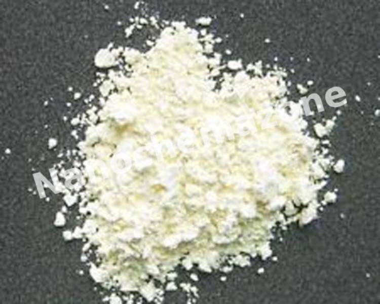
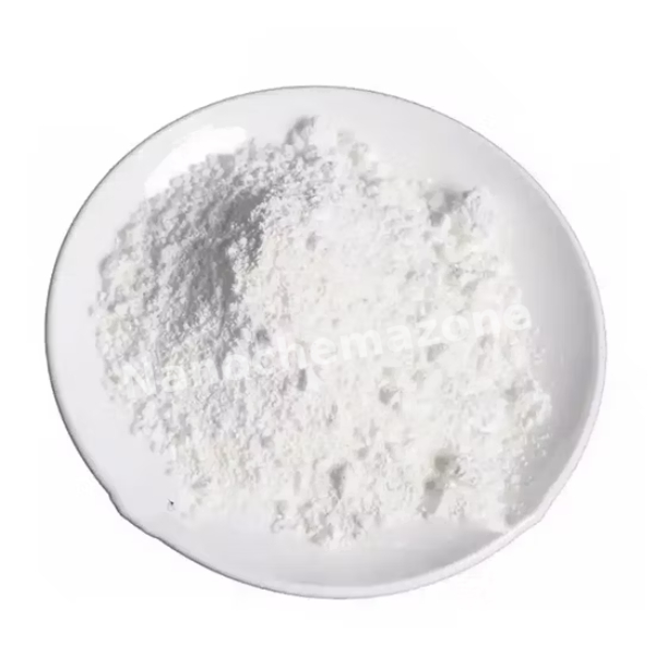
Product Name: ScAl3C3 MAXene Powder

Product ScAl3C3 MAXene Powder
CAS No. 12316-56-2
Appearance Powder
Purity 99%
APS 1 – 5 microns (can be customized)
Ingredient ScAl3C3
Product Code NCZ-MX-319

ScAl3C3 MAXene Powder INTRODUCTION

MAX phase ceramics (including titanium silicon carbide, Ti3AlC2 materials, etc.) are a new type of processing conductive ceramic materials that have attracted much attention. These ceramics contain more than sixty kinds of ternary carbides or nitrides. M represents the transitional front metal elements. ; A represents the main group element, mainly the elements of the third main group and the fourth main group; X represents a carbon or nitrogen element. Among them, Ti3SiC2 is the most widely studied. Ti3SiC2 was successfully synthesized by hot pressing method in 1996 by Professor Barsoum M of Drexel University in the United States, and its excellent performance was found. Due to the unique nano-layered crystal structure, these ceramic materials have antioxidant, self-lubricating properties, high room temperature fracture toughness and electrical conductivity. Such materials can be widely used as high temperature structural materials, electrode brush materials, chemical anticorrosive materials and high temperature heating elements. The products are mainly used for high temperature coating, MXene precursor, conductive self-lubricating ceramic, lithium ion battery, super capacitor, electrochemical catalysis.   RELATED INFORMATION Storage Conditions: Airtight sealed, avoid light, and keep dry at room temperature. Please email us for the customization. Email: contact@nanochemazone.com

Scandium (Sc) Micron Powder Purity: 99.5 %, Size: 325 mesh

Price range: $101.00 through $2,794.00
Select options This product has multiple variants. The options may be chosen on the product page
1 gram/90 € 5 grams/294 € 25 grams/885 € 100 grams/2479 €    

Scandium (Sc) Micron Powder Purity: 99.9 %, Particle Size: 200 mesh

Price range: $96.00 through $2,660.00
Select options This product has multiple variants. The options may be chosen on the product page
1 gram/86 € 5 grams/290 € 25 grams/864 € 100 grams/2360 €      

Scandium (Sc) Micron Powder, Purity: 99.5 %, Size: 325 mesh

Price range: $141.00 through $3,874.00
Select options This product has multiple variants. The options may be chosen on the product page

Applications:

Scandium is one of the transition metals. It is oxidized in air giving yellow or pinkish color. Scandium is found in over 800 mineral species. It can be found in concentrated amounts in the minerals euxenite, gadolinite and thortveitite. Scandium is mainly applied in aluminum scandium alloys. Its light weight makes it suitable for minor aerospace industry components. 

Scandium (Sc) Micron Powder, Purity: 99.9 %, Particle Size: 200 mesh

Price range: $135.00 through $3,687.00
Select options This product has multiple variants. The options may be chosen on the product page

Applications:

Scandium is one of the transition metals. Scandium is oxidized in air giving yellow or pinkish color. Scandium is found in over 800 mineral species. It can be found in concentrated amounts in the minerals euxenite, gadolinite and thortveitite.Scandium is mainly applied in aluminum scandium alloys. Scandium's light weight makes Scandium  suitable for minor aerospace industry components. 

Scandium (Sc) Sputtering Target

Price range: $927.00 through $2,148.00
Select options This product has multiple variants. The options may be chosen on the product page

Product 

Scandium (Sc) Sputtering Target

CAS No.

7440-20-2

Appearance

Powder

Purity

≥99%,  ≥99.9%,  ≥95%

(Other purities are also available)

APS

 NA (Size Can be customized), Ask for other available size ranges.

Ingredient

N/A

Molecular Weight

44.96 g/mol

Melting Point

 1,541 °C

Boiling Point

 2,838 °C

Density

2.99 g/cm³

Product Codes

NCZ-1359K

Scandium ACAC

Price range: $16.00 through $111.00
Select options This product has multiple variants. The options may be chosen on the product page
Product Scandium ACAC
CAS No. 14284-94-7
Appearance White, volatile solid
Purity ≥99%,  ≥99.9%,  ≥95%(Other purities are also available)
APS N/A
Ingredient Sc(C₅H₇O₂)₃
Molecular Weight 342.28 g/mol
Melting Point N/A
Boiling Point N/A
Density 1.385 g/cm³
Product Codes NCZ-295R

Scandium HFAC

Price range: $35.00 through $200.00
Select options This product has multiple variants. The options may be chosen on the product page
Product Scandium HFAC
CAS No. 18990-42-6 
Appearance Powder solid
Purity ≥99%,  ≥99.9%,  ≥95%(Other purities are also available)
APS N/A
Ingredient C₁₅H₃F₁₈O₆Sc
Molecular Weight 666.10–666.11 g/mol
Melting Point 90 °C
Boiling Point N/A
Density N/A
Product Codes NCZ-327R
 

Scandium Oxide (Sc2O3) Micron Powder, Purity: 99.99%, Size: 325 mesh

Price range: $117.00 through $2,141.00
Select options This product has multiple variants. The options may be chosen on the product page

Applications:

Scandium oxide is used in the preparation of other scandium compounds. It is also used as additive to glass, ceramics and high temperature systems to improve their properties.

Scandium TMHD

Price range: $29.00 through $174.00
Select options This product has multiple variants. The options may be chosen on the product page
Product Scandium TMHD
CAS No. 307532-33-8
Appearance White
Purity ≥99%,  ≥99.9%,  ≥95%(Other purities are also available)
APS N/A
Ingredient C₃₃H₅₇O₆Sc
Molecular Weight N/A
Melting Point 150–152 °C
Boiling Point 275 °C
Density N/A
Product Codes NCZ-362R

Scandium(III) oxide (Sc2O3) 99.99% 4N Powder

Price range: $315.00 through $3,010.00
Select options This product has multiple variants. The options may be chosen on the product page
Product Scandium(III) oxide (Sc2O3) 99.99% 4N Powder
CAS No. 12060-08-1
Appearance White
Purity ≥99%,  ≥99.9%,  ≥95%(Other purities are also available)
APS 5µm (Size Can be customized),  Ask for other available size range.
Ingredient Sc2O3
Molecular Weight 137.91 g/mol
Melting Point 2485°C
Boiling Point N/A
Density 3.86 g/cm³
Product Codes NCZ-511I
 

Scandium(III) oxide (Sc2O3) 99.999% 5N Powder

Price range: $503.00 through $3,945.00
Select options This product has multiple variants. The options may be chosen on the product page
Product Scandium(III) oxide (Sc2O3) 99.999% 5N Powder
CAS No. 12060-08-1
Appearance White
Purity ≥99%,  ≥99.9%,  ≥95%(Other purities are also available)
APS 5µm (Size Can be customized),  Ask for other available size range.
Ingredient Sc2O3
Molecular Weight 137.91 g/mol
Melting Point 2485°C
Boiling Point N/A
Density 3.86 g/cm³
Product Codes NCZ-512I

Selenium (Se) Micron Powder Purity: 99.9%, Size: 325 mesh

Price range: $27.00 through $541.00
Select options This product has multiple variants. The options may be chosen on the product page
5 grams/24 € 25 grams/56 €                        
100 grams/122 €                     
500 grams/295 €                     
1000 grams/490 €

Purity: 99.9%, Size: 325 mesh

Selenium (Se) Nanopowder/Nanoparticles, Purity: 99.5+%, Size: < 100 nm

Price range: $1,577.00 through $4,971.00
Select options This product has multiple variants. The options may be chosen on the product page
25 grams/1390 €                       
100 grams/4380 €
Please contact us for quotes on larger quantities !!!

Selenium (Se) Nanopowder/Nanoparticles

Purity: 99.5+%, Size: < 100 nm

Selenium (Se) Nanopowder/Nanoparticles, Purity: 99.5+%, Size: < 100 nm

Price range: $1,577.69 through $5,770.00
Select options This product has multiple variants. The options may be chosen on the product page
Description 25 grams/1390 €                        100 grams/4380 € Please contact us for

Selenium (Se) Sputtering Target

Price range: $261.00 through $923.00
Select options This product has multiple variants. The options may be chosen on the product page

Product 

Selenium (Se) Sputtering Target

CAS No.

7782‑49‑2

Appearance

Powder

Purity

≥99%,  ≥99.9%,  ≥95%

(Other purities are also available)

APS

 NA (Size Can be customized), Ask for other available size ranges.

Ingredient

N/A

Molecular Weight

~78.96 u/g·mol

Melting Point

~217 °C

Boiling Point

~685 °C

Density

~4.79 g/cm³

Product Codes

NCZ-1303K

Selenium (Se) Sputtering Targets, elastomer, Purity: 99.999%, Size: 2”, Thickness: 0.125”

$312.00

Applications of Sputtering Targets;

Film deposition is accomplished using sputtering targets. A technique for sputtering thin films is called "deposition made by sputter targets," which entails eroding material from a "target" source onto a "substrate" like a silicon wafer. Etching of the target is done using semiconductor sputtering targets. When selectivity is not an issue and a high degree of etching anisotropy is required, sputter etching is the method of choice. By removing the target material through etching, sputter targets are also utilized for investigation. In secondary ion spectroscopy (SIMS), one example is when the target material is sputtered at a steady pace. Mass spectrometry is used to quantify the concentration and identity of spewed atoms as the target is sputtered.

The target material's composition may be ascertained and even very low concentrations of contaminants can be found with the aid of the sputtering target.

There is also an application area for sputtering targets in space. One type of space weathering that alters the chemical and physical characteristics of airless worlds like the Moon and asteroids is sputtering.

Selenium (Se) Sputtering Targets, elastomer, Purity: 99.999%, Size: 2”, Thickness: 0.125”

$362.00

Product 

Selenium (Se) Sputtering Targets, elastomer, Purity: 99.999%, Size: 2'', Thickness: 0.125''

CAS No.

7782-49-2

Appearance

Powder

Purity

≥99%,  ≥99.9%,  ≥95%

(Other purities are also available)

APS

N/A  (Size Can be customized), Ask for other available size ranges.

Ingredient

N/A

Molecular Weight

 78.96 g/mol

Melting Point

 221 °C

Boiling Point

 685 °C

Density

 4.81 g/cm³

Product Codes

NCZ-1767K

Selenium (Se) Sputtering Targets, Purity: 99.999%, Size: 1”, Thickness: 0.250”

$116.00

Applications of Sputtering Targets;

Film deposition is accomplished using sputtering targets. A technique for sputtering thin films is called "deposition made by sputter targets," which entails eroding material from a "target" source onto a "substrate" like a silicon wafer. Etching of the target is done using semiconductor sputtering targets. When selectivity is not an issue and a high degree of etching anisotropy is required, sputter etching is the method of choice. By removing the target material through etching, sputter targets are also utilized for investigation. In secondary ion spectroscopy (SIMS), one example is when the target material is sputtered at a steady pace. Mass spectrometry is used to quantify the concentration and identity of spewed atoms as the target is sputtered.

The target material's composition may be ascertained and even very low concentrations of contaminants can be found with the aid of the sputtering target.

There is also an application area for sputtering targets in space. One type of space weathering that alters the chemical and physical characteristics of airless worlds like the Moon and asteroids is sputtering.

Selenium (Se) Sputtering Targets, Purity: 99.999%, Size: 1”, Thickness: 0.250”

$131.00

Product 

Selenium (Se) Sputtering Targets, Purity: 99.999%, Size: 1'', Thickness: 0.250''

CAS No.

7782-49-2

Appearance

Powder

Purity

≥99%,  ≥99.9%,  ≥95%

(Other purities are also available)

APS

N/A  (Size Can be customized), Ask for other available size ranges.

Ingredient

N/A

Molecular Weight

 78.96 g/mol

Melting Point

 221 °C

Boiling Point

 685 °C

Density

 4.81 g/cm³

Product Codes

NCZ-1773K

Selenium (Se) Sputtering Targets, Purity: 99.999%, Size: 2”, Thickness: 0.125”

$495.00

Applications of Sputtering Targets;

Film deposition is accomplished using sputtering targets. A technique for sputtering thin films is called "deposition made by sputter targets," which entails eroding material from a "target" source onto a "substrate" like a silicon wafer. Etching of the target is done using semiconductor sputtering targets. When selectivity is not an issue and a high degree of etching anisotropy is required, sputter etching is the method of choice. By removing the target material through etching, sputter targets are also utilized for investigation. In secondary ion spectroscopy (SIMS), one example is when the target material is sputtered at a steady pace. Mass spectrometry is used to quantify the concentration and identity of spewed atoms as the target is sputtered.

Selenium (Se) Sputtering Targets, Purity: 99.999%, Size: 2”, Thickness: 0.125”

$577.00

Product 

Selenium (Se) Sputtering Targets, Purity: 99.999%, Size: 2'', Thickness: 0.125''

CAS No.

7782-49-2

Appearance

Powder

Purity

≥99%,  ≥99.9%,  ≥95%

(Other purities are also available)

APS

N/A  (Size Can be customized), Ask for other available size ranges.

Ingredient

N/A

Molecular Weight

 78.96 g/mol

Melting Point

 221 °C

Boiling Point

 685 °C

Density

 4.81 g/cm³

Product Codes

NCZ-1772K

Selenium (Se) Sputtering Targets, Purity: 99.999%, Size: 2”, Thickness: 0.250”

$470.00

Applications of Sputtering Targets;

Film deposition is accomplished using sputtering targets. A technique for sputtering thin films is called "deposition made by sputter targets," which entails eroding material from a "target" source onto a "substrate" like a silicon wafer. Etching of the target is done using semiconductor sputtering targets. When selectivity is not an issue and a high degree of etching anisotropy is required, sputter etching is the method of choice. By removing the target material through etching, sputter targets are also utilized for investigation. In secondary ion spectroscopy (SIMS), one example is when the target material is sputtered at a steady pace. Mass spectrometry is used to quantify the concentration and identity of spewed atoms as the target is sputtered.

The target material's composition may be ascertained and even very low concentrations of contaminants can be found with the aid of the sputtering target.

There is also an application area for sputtering targets in space. One type of space weathering that alters the chemical and physical characteristics of airless worlds like the Moon and asteroids is sputtering.

Selenium (Se) Sputtering Targets, Purity: 99.999%, Size: 2”, Thickness: 0.250”

$248.00

Product 

Selenium (Se) Sputtering Targets, Purity: 99.999%, Size: 2'', Thickness: 0.250''

CAS No.

7782-49-2

Appearance

Powder

Purity

≥99%,  ≥99.9%,  ≥95%

(Other purities are also available)

APS

N/A  (Size Can be customized), Ask for other available size ranges.

Ingredient

N/A

Molecular Weight

 78.96 g/mol

Melting Point

 221 °C

Boiling Point

 685 °C

Density

 4.81 g/cm³

Product Codes

NCZ-1771K

Selenium (Se) Sputtering Targets, Purity: 99.999%, Size: 3”, Thickness: 0.125”

$288.00

Applications of Sputtering Targets;

Film deposition is accomplished using sputtering targets. A technique for sputtering thin films is called "deposition made by sputter targets," which entails eroding material from a "target" source onto a "substrate" like a silicon wafer. Etching of the target is done using semiconductor sputtering targets. When selectivity is not an issue and a high degree of etching anisotropy is required, sputter etching is the method of choice. By removing the target material through etching, sputter targets are also utilized for investigation. In secondary ion spectroscopy (SIMS), one example is when the target material is sputtered at a steady pace. Mass spectrometry is used to quantify the concentration and identity of spewed atoms as the target is sputtered.

The target material's composition may be ascertained and even very low concentrations of contaminants can be found with the aid of the sputtering target.

There is also an application area for sputtering targets in space. One type of space weathering that alters the chemical and physical characteristics of airless worlds like the Moon and asteroids is sputtering.

Selenium (Se) Sputtering Targets, Purity: 99.999%, Size: 3”, Thickness: 0.125”

$334.00

Product 

Selenium (Se) Sputtering Targets, Purity: 99.999%, Size: 3'', Thickness: 0.125''

CAS No.

7782-49-2

Appearance

Powder

Purity

≥99%,  ≥99.9%,  ≥95%

(Other purities are also available)

APS

N/A  (Size Can be customized), Ask for other available size ranges.

Ingredient

N/A

Molecular Weight

 78.96 g/mol

Melting Point

 221 °C

Boiling Point

 685 °C

Density

 4.81 g/cm³

Product Codes

NCZ-1770K

Selenium (Se) Sputtering Targets, Purity: 99.999%, Size: 3”, Thickness: 0.250”

$327.00

Applications of Sputtering Targets;

Film deposition is accomplished using sputtering targets. A technique for sputtering thin films is called "deposition made by sputter targets," which entails eroding material from a "target" source onto a "substrate" like a silicon wafer. Etching of the target is done using semiconductor sputtering targets. When selectivity is not an issue and a high degree of etching anisotropy is required, sputter etching is the method of choice. By removing the target material through etching, sputter targets are also utilized for investigation. In secondary ion spectroscopy (SIMS), one example is when the target material is sputtered at a steady pace. Mass spectrometry is used to quantify the concentration and identity of spewed atoms as the target is sputtered.

Selenium (Se) Sputtering Targets, Purity: 99.999%, Size: 3”, Thickness: 0.250”

$380.00

Product 

Selenium (Se) Sputtering Targets, Purity: 99.999%, Size: 3'', Thickness: 0.250''

CAS No.

7782-49-2

Appearance

Powder

Purity

≥99%,  ≥99.9%,  ≥95%

(Other purities are also available)

APS

N/A  (Size Can be customized), Ask for other available size ranges.

Ingredient

N/A

Molecular Weight

 78.96 g/mol

Melting Point

 221 °C

Boiling Point

 685 °C

Density

 4.81 g/cm³

Product Codes

NCZ-1769K

Selenium (Se) Sputtering Targets, Purity: 99.999%, Size: 4”, Thickness: 0.125”

$290.00

Applications of Sputtering Targets;

Film deposition is accomplished using sputtering targets. A technique for sputtering thin films is called "deposition made by sputter targets," which entails eroding material from a "target" source onto a "substrate" like a silicon wafer. Etching of the target is done using semiconductor sputtering targets. When selectivity is not an issue and a high degree of etching anisotropy is required, sputter etching is the method of choice. By removing the target material through etching, sputter targets are also utilized for investigation. In secondary ion spectroscopy (SIMS), one example is when the target material is sputtered at a steady pace. Mass spectrometry is used to quantify the concentration and identity of spewed atoms as the target is sputtered.

The target material's composition may be ascertained and even very low concentrations of contaminants can be found with the aid of the sputtering target.

There is also an application area for sputtering targets in space. One type of space weathering that alters the chemical and physical characteristics of airless worlds like the Moon and asteroids is sputtering.

Selenium (Se) Sputtering Targets, Purity: 99.999%, Size: 4”, Thickness: 0.125”

$336.00

Product 

Selenium (Se) Sputtering Targets, Purity: 99.999%, Size: 4'', Thickness: 0.250''

CAS No.

7782-49-2

Appearance

Powder

Purity

≥99%,  ≥99.9%,  ≥95%

(Other purities are also available)

APS

N/A  (Size Can be customized), Ask for other available size ranges.

Ingredient

N/A

Molecular Weight

 78.96 g/mol

Melting Point

 221 °C

Boiling Point

 685 °C

Density

 4.81 g/cm³

Product Codes

NCZ-1768K

Selenium (Se) Sputtering Targets, Purity: 99.999%, Size: 4”, Thickness: 0.250”

$537.00

Applications of Sputtering Targets;

Film deposition is accomplished using sputtering targets. A technique for sputtering thin films is called "deposition made by sputter targets," which entails eroding material from a "target" source onto a "substrate" like a silicon wafer. Etching of the target is done using semiconductor sputtering targets. When selectivity is not an issue and a high degree of etching anisotropy is required, sputter etching is the method of choice. By removing the target material through etching, sputter targets are also utilized for investigation. In secondary ion spectroscopy (SIMS), one example is when the target material is sputtered at a steady pace. Mass spectrometry is used to quantify the concentration and identity of spewed atoms as the target is sputtered.

The target material's composition may be ascertained and even very low concentrations of contaminants can be found with the aid of the sputtering target.

There is also an application area for sputtering targets in space. One type of space weathering that alters the chemical and physical characteristics of airless worlds like the Moon and asteroids is sputtering.

Selenium (Se) Sputtering Targets, Purity: 99.999%, Size: 4”, Thickness: 0.250”

$627.00

Product 

Selenium (Se) Sputtering Targets, Purity: 99.999%, Size: 4'', Thickness: 0.250''

CAS No.

7782-49-2

Appearance

Powder

Purity

≥99%,  ≥99.9%,  ≥95%

(Other purities are also available)

APS

N/A  (Size Can be customized), Ask for other available size ranges.

Ingredient

N/A

Molecular Weight

 78.96 g/mol

Melting Point

 221 °C

Boiling Point

 685 °C

Density

 4.81 g/cm³

Product Codes

NCZ-1768K

Selenium (Se) Sputtering Targets, Purity: 99.999%, Size:1”, Thickness: 0.125”

$116.00

Applications of Sputtering Targets;

Film deposition is accomplished using sputtering targets. A technique for sputtering thin films is called "deposition made by sputter targets," which entails eroding material from a "target" source onto a "substrate" like a silicon wafer. Etching of the target is done using semiconductor sputtering targets. When selectivity is not an issue and a high degree of etching anisotropy is required, sputter etching is the method of choice. By removing the target material through etching, sputter targets are also utilized for investigation. In secondary ion spectroscopy (SIMS), one example is when the target mat

The target material's composition may be ascertained and even very low concentrations of contaminants can be found with the aid of the sputtering target.

There is also an application area for sputtering targets in space. One type of space weathering that alters the chemical and physical characteristics of airless worlds like the Moon and asteroids is sputtering.

erial is sputtered at a steady pace. Mass spectrometry is used to quantify the concentration and identity of spewed atoms as the target is sputtered.

Selenium (Se) Sputtering Targets, Purity: 99.999%, Size:1”, Thickness: 0.125”

$131.00

Product 

Selenium (Se) Sputtering Targets, Purity: 99.999%, Size:1'', Thickness: 0.125''

CAS No.

7782-49-2

Appearance

Powder

Purity

≥99%,  ≥99.9%,  ≥95%

(Other purities are also available)

APS

N/A  (Size Can be customized), Ask for other available size ranges.

Ingredient

N/A

Molecular Weight

 78.96 g/mol

Melting Point

 221 °C

Boiling Point

 685 °C

Density

 4.81 g/cm³

Product Codes

NCZ-1774K

Selenium Sputtering Target Se

Price range: $329.00 through $759.00
Select options This product has multiple variants. The options may be chosen on the product page
Product Selenium Sputtering Target Se
CAS No. 7782-49-2
Appearance Gray, Metallic Luster, Non-Metallic
Purity ≥99%,  ≥99.9%,  ≥95%(Other purities are also available)
APS 1–10 µm (Size Can be customized),  Ask for other available size range.
Ingredient Se
Molecular Weight 78.96 g/mol
Melting Point N/A
Boiling Point N/A
Density 4.79 g/cm
Product Codes NCZ-135H
 

Shape Memory Polymer NGM2520, Ether Type

Price range: $495.00 through $6,175.00
Select options This product has multiple variants. The options may be chosen on the product page

Applications:

Shape Memory Polymer (SMP) has myriad of advanced applications in different fields from daily life uses like textile to biomedicals. These applications include smart catheter, drug-delivery systems, biosensors, auto-repairing automobile parts, smart textile, self-healing materials, smart suture, artificial organs like muscles, and so on.

Shape Memory Polymer NGM3520, Ether Type

Price range: $603.75 through $7,633.75
Select options This product has multiple variants. The options may be chosen on the product page

Applications:

Shape Memory Polymer (SMP) has myriad of advanced applications in different fields from daily life uses like textile to biomedicals. These applications include smart catheter, drug-delivery systems, biosensors, auto-repairing automobile parts, smart textile, self-healing materials, smart suture, artificial organs like muscles, and so on.

Shape Memory Polymer NGM4520, Ether Type

Price range: $475.00 through $6,094.00
Select options This product has multiple variants. The options may be chosen on the product page

Applications:

Shape Memory Polymer (SMP) has myriad of advanced applications in different fields from daily life uses like textile to biomedicals. These applications include smart catheter, drug-delivery systems, biosensors, auto-repairing automobile parts, smart textile, self-healing materials, smart suture, artificial organs like muscles, and so on.

Shape Memory Polymer NGM5520, Ether Type

Price range: $457.00 through $6,057.00
Select options This product has multiple variants. The options may be chosen on the product page

Applications:

Shape Memory Polymer (SMP) has myriad of advanced applications in different fields from daily life uses like textile to biomedicals. These applications include smart catheter, drug-delivery systems, biosensors, auto-repairing automobile parts, smart textile, self-healing materials, smart suture, artificial organs like muscles, and so on.

Shape Memory Polymer NGM6520, Ether Type

Price range: $450.00 through $6,032.00
Select options This product has multiple variants. The options may be chosen on the product page

Applications:

Shape Memory Polymer (SMP) has myriad of advanced applications in different fields from daily life uses like textile to biomedicals. These applications include smart catheter, drug-delivery systems, biosensors, auto-repairing automobile parts, smart textile, self-healing materials, smart suture, artificial organs like muscles, and so on.

Shape Memory Polymer NGM7520, Ether Type

Price range: $432.00 through $5,988.00
Select options This product has multiple variants. The options may be chosen on the product page

Applications:

Shape Memory Polymer (SMP) has myriad of advanced applications in different fields from daily life uses like textile to biomedicals. These applications include smart catheter, drug-delivery systems, biosensors, auto-repairing automobile parts, smart textile, self-healing materials, smart suture, artificial organs like muscles, and so on.

Shape Memory Polymer NGM9020, Ether Type

Price range: $425.00 through $5,963.00
Select options This product has multiple variants. The options may be chosen on the product page

Applications:

Shape Memory Polymer (SMP) has myriad of advanced applications in different fields from daily life uses like textile to biomedicals. These applications include smart catheter, drug-delivery systems, biosensors, auto-repairing automobile parts, smart textile, self-healing materials, smart suture, artificial organs like muscles, and so on.

Shape Memory Polymer NGP2510, Potting Type

Price range: $2,482.00 through $8,588.00
Select options This product has multiple variants. The options may be chosen on the product page

Applications:

Shape Memory Polymer (SMP) has myriad of advanced applications in different fields from daily life uses like textile to biomedicals. These applications include smart catheter, drug-delivery systems, biosensors, auto-repairing automobile parts, smart textile, self-healing materials, smart suture, artificial organs like muscles, and so on.

Shape Memory Polymer NGP3510, Potting Type

Price range: $2,482.00 through $8,588.00
Select options This product has multiple variants. The options may be chosen on the product page

Applications:

Shape Memory Polymer (SMP) has myriad of advanced applications in different fields from daily life uses like textile to biomedicals. These applications include smart catheter, drug-delivery systems, biosensors, auto-repairing automobile parts, smart textile, self-healing materials, smart suture, artificial organs like muscles, and so on.

Shape Memory Polymer NGP4510, Potting Type

Price range: $2,482.00 through $8,588.00
Select options This product has multiple variants. The options may be chosen on the product page

Applications:

Shape Memory Polymer (SMP) has myriad of advanced applications in different fields from daily life uses like textile to biomedicals. These applications include smart catheter, drug-delivery systems, biosensors, auto-repairing automobile parts, smart textile, self-healing materials, smart suture, artificial organs like muscles, and so on.

Shape Memory Polymer NGP5510, Potting Type

Price range: $2,482.00 through $8,588.00
Select options This product has multiple variants. The options may be chosen on the product page

Applications:

Shape Memory Polymer (SMP) has myriad of advanced applications in different fields from daily life uses like textile to biomedicals. These applications include smart catheter, drug-delivery systems, biosensors, auto-repairing automobile parts, smart textile, self-healing materials, smart suture, artificial organs like muscles, and so on.

Shape Memory Polymer NGS2520, Solution Type

Price range: $432.00 through $6,232.00
Select options This product has multiple variants. The options may be chosen on the product page

Applications:

Shape Memory Polymer (SMP) has myriad of advanced applications in different fields from daily life uses like textile to biomedicals. These applications include smart catheter, drug-delivery systems, biosensors, auto-repairing automobile parts, smart textile, self-healing materials, smart suture, artificial organs like muscles, and so on.