1 piece/53 €
5 pieces/225 €
25 pieces/1050 €
Please contact us for quotes on larger quantities !!!
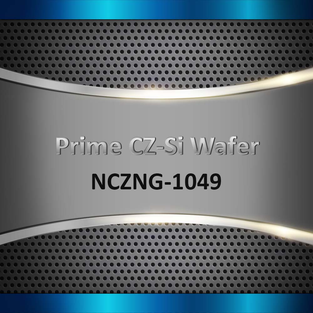
Prime CZ-Si Wafer
Size: 6”, Orientation: (100), Boron Doped, 1-Side Polished, Thickness: 675 ± 15 μm
Technical Properties:
| Quality |
Prime |
| Materials |
CZ-Si |
| Size (inch) |
6” |
| Orientation |
(100) |
| Coating |
|
| Thickness (μm) |
675 ± 15 |
| Doping |
Boron |
| Resistivity (ohm.cm) |
1-10 |
| Polished |
One Side |
Silicon is one of the most common elements on earths crust. Main usage of Silicon wafers is electronics and technology. Silicon wafers have very flat and mirror like surfaces. It is produced by Czochralski method to obtain the highest purity. Depending on the usage area, silicon wafers can be doped with different materials to tailor its purity accordingly. The amount and type of dopants highly affect the electronic properties. Galium, indium, boron and nitrogen are some of the dopants that can be used in production process.
Silicon wafers are used in semiconductors, microchips, integrated circuits, smartphones, computers etc. Silicon is the key platform for semiconductor gadgets. A wafer is just but a thin slice of the semiconductor material that acts as a substratum for microelectronic devices fitted in and above the wafer.