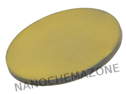
Magnesium Fluoride (MgF2) Sputtering Targets, Purity: 99.9%, Size: 2”, Thickness: 0.125”

$495.00

Applications of Sputtering Targets;

Film deposition is accomplished using sputtering targets. A technique for sputtering thin films is called "deposition made by sputter targets," which entails eroding material from a "target" source onto a "substrate" like a silicon wafer. Etching of the target is done using semiconductor sputtering targets. When selectivity is not an issue and a high degree of etching anisotropy is required, sputter etching is the method of choice. By removing the target material through etching, sputter targets are also utilized for investigation. In secondary ion spectroscopy (SIMS), one example is when the target material is sputtered at a steady pace. Mass spectrometry is used to quantify the concentration and identity of spewed atoms as the target is sputtered.

By helping of the sputtering target, the composition of the target material may be evaluated and even extremely tiny amounts of contaminants are recognized.

There is also an application area for sputtering targets in space. One type of space weathering that alters the chemical and physical characteristics of airless worlds like the Moon and asteroids is sputtering.

Magnesium Fluoride (MgF2) Sputtering Targets, Purity: 99.9%, Size: 4”, Thickness: 0.250”

$495.00

Film deposition is accomplished using sputtering targets. A technique for sputtering thin films is called "deposition made by sputter targets," which entails eroding material from a "target" source onto a "substrate" like a silicon wafer. Etching of the target is done using semiconductor sputtering targets. When selectivity is not an issue and a high degree of etching anisotropy is required, sputter etching is the method of choice. By removing the target material through etching, sputter targets are also utilized for investigation. In secondary ion spectroscopy (SIMS), one example is when the target material is sputtered at a steady pace. Mass spectrometry is used to quantify the concentration and identity of spewed atoms as the target is sputtered.

By helping of the sputtering target, the composition of the target material may be evaluated and even extremely tiny amounts of contaminants are recognized.

There is also an application area for sputtering targets in space. One type of space weathering that alters the chemical and physical characteristics of airless worlds like the Moon and asteroids is sputtering.

Nickel Chromium (Ni-Cr) Sputtering Targets, Purity: 99.9%, Size: 4”, Thickness: 0.250”

$495.00

Applications of Sputtering Targets;

Film deposition is done using puttering targets. A technique for sputtering thin films is called "deposition made by sputter targets," which entails eroding material from a "target" source onto a "substrate" like a silicon wafer. Etching of the target is done using semiconductor sputtering targets. When selectivity is not an issue and a high degree of etching anisotropy is required, sputter etching is the method of choice. By removing the target material through etching, sputter targets are also utilized for investigation. In secondary ion spectroscopy (SIMS), one example is when the target material is sputtered at a steady pace. Mass spectrometry is used to quantify the concentration and identity of spewed atoms as the target is sputtered.

The target material's composition may be ascertained and even very low concentrations of contaminants can be found with the aid of the sputtering target.

There is also an application area for sputtering targets in space. One type of space weathering that alters the chemical and physical characteristics of airless worlds like the Moon and asteroids is sputtering.

Nickel Chromium (Ni-Cr) Sputtering Targets, Purity: 99.95%, Size: 6”, Thickness: 0.125”

$495.00

Applications of Sputtering Targets;

Film deposition is accomplished using sputtering targets. A technique for sputtering thin films is called "deposition made by sputter targets," which entails eroding material from a "target" source onto a "substrate" like a silicon wafer. Etching of the target is done using semiconductor sputtering targets. When selectivity is not an issue and a high degree of etching anisotropy is required, sputter etching is the method of choice. By removing the target material through etching, sputter targets are also utilized for investigation. In secondary ion spectroscopy (SIMS), one example is when the target material is sputtered at a steady pace. Mass spectrometry is used to quantify the concentration and identity of spewed atoms as the target is sputtered.

The target material's composition may be ascertained and even very low concentrations of contaminants can be found with the aid of the sputtering target.

There is also an application area for sputtering targets in space. One type of space weathering that alters the chemical and physical characteristics of airless worlds like the Moon and asteroids is sputtering.

Selenium (Se) Sputtering Targets, Purity: 99.999%, Size: 2”, Thickness: 0.125”

$495.00

Applications of Sputtering Targets;

Film deposition is accomplished using sputtering targets. A technique for sputtering thin films is called "deposition made by sputter targets," which entails eroding material from a "target" source onto a "substrate" like a silicon wafer. Etching of the target is done using semiconductor sputtering targets. When selectivity is not an issue and a high degree of etching anisotropy is required, sputter etching is the method of choice. By removing the target material through etching, sputter targets are also utilized for investigation. In secondary ion spectroscopy (SIMS), one example is when the target material is sputtered at a steady pace. Mass spectrometry is used to quantify the concentration and identity of spewed atoms as the target is sputtered.

Titanium Dioxide (TiO2) Anatase Phase Nanofibers, 1g/bottle

$495.00
Product Titanium Dioxide (TiO2) Anatase Phase Nanofibers, 1g/bottle
CAS No. 13463-67-7
Appearance White, fibrous
Purity ≥99%,  ≥99.9%,  ≥95%(Other purities are also available)
APS 100–200nm (Size Can be customized),  Ask for other available size range.
Ingredient TiO2
Molecular Weight N/A
Melting Point N/A
Boiling Point N/A
Density N/A
Product Codes NCZ-577I

Boron (B) Sputtering Targets, elastomer, Purity: 99.9%, Size: 2”, Thickness: 0.125”

$496.00

Applications of Sputtering Targets;

Film deposition is accomplished using sputtering targets. A technique for sputtering thin films is called "deposition made by sputter targets," which entails eroding material from a "target" source onto a "substrate" like a silicon wafer. Etching of the target is done using semiconductor sputtering targets. When selectivity is not an issue and a high degree of etching anisotropy is required, sputter etching is the method of choice. By removing the target material through etching, sputter targets are also utilized for investigation. In secondary ion spectroscopy (SIMS), one example is when the target material is sputtered at a steady pace. Mass spectrometry is used to quantify the concentration and identity of spewed atoms as the target is sputtered.

The target material's composition may be ascertained and even very low concentrations of contaminants can be found with the aid of the sputtering target.

There is also an application area for sputtering targets in space. One type of space weathering that alters the chemical and physical characteristics of airless worlds like the Moon and asteroids is sputtering.

Boron Nitride (BN) Sputtering Targets, Purity: 99.5%, Size: 2”, Thickness: 0.250”

$496.00

Applications of Sputtering Targets;

Film deposition is accomplished using sputtering targets. A technique for sputtering thin films is called "deposition made by sputter targets," which entails eroding material from a "target" source onto a "substrate" like a silicon wafer. Etching of the target is done using semiconductor sputtering targets. When selectivity is not an issue and a high degree of etching anisotropy is required, sputter etching is the method of choice. By removing the target material through etching, sputter targets are also utilized for investigation. In secondary ion spectroscopy (SIMS), one example is when the target material is sputtered at a steady pace. Mass spectrometry is used to quantify the concentration and identity of spewed atoms as the target is sputtered.

The target material's composition may be ascertained and even very low concentrations of contaminants can be found with the aid of the sputtering target.

There is also an application area for sputtering targets in space. One type of space weathering that alters the chemical and physical characteristics of airless worlds like the Moon and asteroids is sputtering.

Silicon (Si) Sputtering Targets, N-type, Purity: 99.999%, Size: 6”, Thickness: 0.250”

$496.00

Product 

Silicon (Si) Sputtering Targets, N-type, Purity: 99.999%, Size: 6'', Thickness: 0.250''

CAS No.

7440-21-3

Appearance

Powder

Purity

≥99%,  ≥99.9%,  ≥95%

(Other purities are also available)

APS

N/A  (Size Can be customized), Ask for other available size ranges.

Ingredient

N/A

Molecular Weight

28.0855 g/mol

Melting Point

 1,414 °C

Boiling Point

3,265 °C

Density

 2.33 g/cm³

Product Codes

NCZ-1756K

3N5 (99.95%) Iron (Fe) Pellets Evaporation Materials

Price range: $497.00 through $717.00
Select options This product has multiple variants. The options may be chosen on the product page
Product 3N5 (99.95%) Iron (Fe) Pellets Evaporation Materials
CAS No. 7439-89-6
Appearance Lustrous, Metallic, Grayish Tinge 
Purity ≥99%,  ≥99.9%,  ≥95%(Other purities are also available)
APS 3–10 mm (Size Can be customized),  Ask for other available size range.
Ingredient Fe
Molecular Weight 95.96 g/mol
Melting Point 1535°C
Boiling Point 3000°C
Density 7.86 g/cm³
Product Codes NCZ-120E

3N (99.9%) Titanium Dioxide (TiO2) White Pieces (3-6mm) Evaporation Materials

Price range: $497.00 through $717.00
Select options This product has multiple variants. The options may be chosen on the product page
Product 3N (99.9%) Titanium Dioxide (TiO2) White Pieces (3-6mm) Evaporation Materials
CAS No. 13463-67-7
Appearance White-Beige, Gray-Black 
Purity ≥99%,  ≥99.9%,  ≥95%(Other purities are also available)
APS 3-6mm (Size Can be customized),  Ask for other available size range.
Ingredient TiO2
Molecular Weight 79.9 g/mol
Melting Point 1,830°C
Boiling Point N/A
Density 7.86 g/cm³
Product Codes NCZ-121E

Tungsten Titanium (TiW) Sputtering Targets, Purity: 99.99%, Size: 8”, Thickness: 0.250”

$497.00

Product 

Tungsten Titanium (TiW) Sputtering Targets, Purity: 99.99%, Size: 8'', Thickness: 0.250''

CAS No.

58397‑70‑9

Appearance

Powder

Purity

≥99%,  ≥99.9%,  ≥95%

(Other purities are also available)

APS

N/A  (Size Can be customized), Ask for other available size ranges.

Ingredient

N/A

Molecular Weight

231.71 g/mol

Melting Point

~2,700–3,400 °C

Boiling Point

~3,167–3,930 °C

Density

~14.5–17.0 g/cm³ (depends on composition and porosity)

Product Codes

NCZ-1552K

Nickel Chromium (Ni-Cr) Sputtering Targets, Purity: 99.95%, Size: 3”, Thickness: 0.250”

$497.00

Product 

Nickel Chromium (Ni-Cr) Sputtering Targets, Purity: 99.95%, Size: 3'', Thickness: 0.250''

CAS No.

 11106-97-1

Appearance

Powder

Purity

≥99%,  ≥99.9%,  ≥95%

(Other purities are also available)

APS

 N/A (Size Can be customized), Ask for other available size ranges.

Ingredient

N/A

Molecular Weight

 ~110.69 g/mol

Melting Point

 ~1,400 °C

Boiling Point

 ~2,730–2,750 °C

Density

 ~8.4 – 8.5 g/cm³

Product Codes

NCZ-1854K

Magnesium (Mg) Sputtering Targets, Purity: 99.95%, Size: 6”, Thickness: 0.250”

$498.00

Product 

Magnesium (Mg) Sputtering Targets, Purity: 99.95%, Size: 6'', Thickness: 0.250''

CAS No.

7439-95-4

Appearance

Powder

Purity

≥99%,  ≥99.9%,  ≥95%

(Other purities are also available)

APS

 N/A (Size Can be customized), Ask for other available size ranges.

Ingredient

N/A

Molecular Weight

 24.305 g/mol

Melting Point

 650 °C

Boiling Point

 1,090 °C

Density

1.738 g/cm³

Product Codes

NCZ-1990K

Lanthanum Calcium Manganate (La0.7Ca0.3MnO3) Sputtering Targets, Purity: 99.9%, Size: 1”, Thickness: 0.250”

$499.00
Select options This product has multiple variants. The options may be chosen on the product page

Applications of Sputtering Targets;

  • Sputtering targets is used for film deposition. The deposition made by sputter targets is a method of depositing thin films by sputtering that involves eroding material from a "target" source onto a "substrate" such as  a silicon wafer.
  • Semiconductor sputtering targets is used to etch the target. Sputter etching is chosen in cases where a high degree of etching anisotropy is needed and selectivity is not a concern.
  • Sputter targets is also used for analysis by etching away the target material.
One of the example occurs in secondary ion spectroscopy (SIMS), where the target sample is sputtered at a constant rate. As the target is sputtered, the concentration and identity of sputtered atoms are measured using mass spectrometry. By helping of the sputtering target, the composition of the target material can be determined and even extremely low concentrations of impurities are detected. Sputtering target has also application area in space. Sputtering is one of the forms of space weathering, a process that changes the physical and chemical properties of airless bodies, such as asteroids and the Moon.

Lanthanum Calcium Manganate (La0.7Ca0.3MnO3) Sputtering Targets, Purity: 99.9%, Size: 1”, Thickness: 0.250”

$499.00

Applications of Sputtering Targets;

Film deposition is accomplished using sputtering targets. A technique for sputtering thin films is called "deposition made by sputter targets," which entails eroding material from a "target" source onto a "substrate" like a silicon wafer. Etching of the target is done using semiconductor sputtering targets. When selectivity is not an issue and a high degree of etching anisotropy is required, sputter etching is the method of choice. By removing the target material through etching, sputter targets are also utilized for investigation. In secondary ion spectroscopy (SIMS), one example is when the target material is sputtered at a steady pace. Mass spectrometry is used to quantify the concentration and identity of spewed atoms as the target is sputtered.

The target material's composition may be ascertained and even very low concentrations of contaminants can be found with the aid of the sputtering target.

There is also an application area for sputtering targets in space. One type of space weathering that alters the chemical and physical characteristics of airless worlds like the Moon and asteroids is sputtering.

Nickel (Ni) Sputtering Targets, Purity: 99.9%, Size: 6”, Thickness: 0.125”

$499.00

Applications of Sputtering Targets;

Film deposition is accomplished using sputtering targets. A technique for sputtering thin films is called "deposition made by sputter targets," which entails eroding material from a "target" source onto a "substrate" like a silicon wafer. Etching of the target is done using semiconductor sputtering targets. When selectivity is not an issue and a high degree of etching anisotropy is required, sputter etching is the method of choice. By removing the target material through etching, sputter targets are also utilized for investigation. In secondary ion spectroscopy (SIMS), one example is when the target material is sputtered at a steady pace. Mass spectrometry is used to quantify the concentration and identity of spewed atoms as the target is sputtered.

The target material's composition may be ascertained and even very low concentrations of contaminants can be found with the aid of the sputtering target.

There is also an application area for sputtering targets in space. One type of space weathering that alters the chemical and physical characteristics of airless worlds like the Moon and asteroids is sputtering.

Aluminum Fluoride (AlF3) Powder 99.99% Optical Grade

$499.00
Select options This product has multiple variants. The options may be chosen on the product page
Product Aluminum Fluoride (AlF3) Powder 99.99% Optical Grade
CAS No. 7784-18-1
Appearance White, odorless solid
Purity ≥99%,  ≥99.9%,  ≥95%(Other purities are also available)
APS 1–10µm (Size Can be customized),  Ask for other available size range.
Ingredient AlF3
Molecular Weight 83.98 g/mol
Melting Point 1,290 °C
Boiling Point N/A
Density 3.10 g/cm³
Product Codes NCZ-280I
 

Praseodymium (Pr) Sputtering Targets, Purity: 99.9%, Size: 6”, Thickness: 0.125”

$500.00

Applications of Sputtering Targets;

  • Sputtering targets is used for film deposition. The deposition made by sputter targets is a method of depositing thin films by sputtering that involves eroding material from a "target" source onto a "substrate" such as  a silicon wafer.
  • Semiconductor sputtering targets is used to etch the target. Sputter etching is chosen in cases where a high degree of etching anisotropy is needed and selectivity is not a concern.
  • Sputter targets is also used for analysis by etching away the target material.
One of the example occurs in secondary ion spectroscopy (SIMS), where the target sample is sputtered at a constant rate. As the target is sputtered, the concentration and identity of sputtered atoms are measured using mass spectrometry. By helping of the sputtering target, the composition of the target material can be determined and even extremely low concentrations of impurities are detected. Sputtering target has also application area in space. Sputtering is one of the forms of space weathering, a process that changes the physical and chemical properties of airless bodies, such as asteroids and the Moon.

Copper (Cu) Sputtering Targets, Purity: 99.999%, Size: 8”, Thickness: 0.250”

$500.00

Applications of Sputtering Targets;

Film deposition is accomplished using sputtering targets. A technique for sputtering thin films is called "deposition made by sputter targets," which entails eroding material from a "target" source onto a "substrate" like a silicon wafer. Etching of the target is done using semiconductor sputtering targets. When selectivity is not an issue and a high degree of etching anisotropy is required, sputter etching is the method of choice. By removing the target material through etching, sputter targets are also utilized for investigation. In secondary ion spectroscopy (SIMS), one example is when the target material is sputtered at a steady pace. Mass spectrometry is used to quantify the concentration and identity of spewed atoms as the target is sputtered.

The target material's composition may be ascertained and even very low concentrations of contaminants can be found with the aid of the sputtering target.

There is also an application area for sputtering targets in space. One type of space weathering that alters the chemical and physical characteristics of airless worlds like the Moon and asteroids is sputtering.

Copper (Cu) Sputtering Targets, Purity: 99.999%, Size: 8”, Thickness: 0.250”

$500.00

Applications of Sputtering Targets;

Film deposition is accomplished using sputtering targets. A technique for sputtering thin films is called "deposition made by sputter targets," which entails eroding material from a "target" source onto a "substrate" like a silicon wafer. Etching of the target is done using semiconductor sputtering targets. When selectivity is not an issue and a high degree of etching anisotropy is required, sputter etching is the method of choice. By removing the target material through etching, sputter targets are also utilized for investigation. In secondary ion spectroscopy (SIMS), one example is when the target material is sputtered at a steady pace. Mass spectrometry is used to quantify the concentration and identity of spewed atoms as the target is sputtered.

The target material's composition may be ascertained and even very low concentrations of contaminants can be found with the aid of the sputtering target.

There is also an application area for sputtering targets in space. One type of space weathering that alters the chemical and physical characteristics of airless worlds like the Moon and asteroids is sputtering.

Praseodymium (Pr) Sputtering Targets, Purity: 99.9%, Size: 6”, Thickness: 0.125”

$500.00

Applications of Sputtering Targets;

Film deposition is accomplished using sputtering targets. A technique for sputtering thin films is called "deposition made by sputter targets," which entails eroding material from a "target" source onto a "substrate" like a silicon wafer. Etching of the target is done using semiconductor sputtering targets. When selectivity is not an issue and a high degree of etching anisotropy is required, sputter etching is the method of choice. By removing the target material through etching, sputter targets are also utilized for investigation. In secondary ion spectroscopy (SIMS), one example is when the target material is sputtered at a steady pace. Mass spectrometry is used to quantify the concentration and identity of spewed atoms as the target is sputtered.

The target material's composition may be ascertained and even very low concentrations of contaminants can be found with the aid of the sputtering target.

There is also an application area for sputtering targets in space. One type of space weathering that alters the chemical and physical characteristics of airless worlds like the Moon and asteroids is sputtering.

Tungsten Disulfide (WS2) Sputtering Targets, Purity: 99.9%, Size: 8”, Thickness: 0.250”

$500.00

Product 

Tungsten Disulfide (WS2) Sputtering Targets, Purity: 99.9%, Size: 8'', Thickness: 0.250''

CAS No.

 12138-09-9

Appearance

Powder

Purity

≥99%,  ≥99.9%,  ≥95%

(Other purities are also available)

APS

N/A  (Size Can be customized), Ask for other available size ranges.

Ingredient

N/A

Molecular Weight

247.97 g/mol

Melting Point

~1,250 °C

Boiling Point

N/A

Density

~7.5 g/cm³

Product Codes

NCZ-1576K

Tantalum Oxide (Ta2O5) Sputtering Targets, Purity: 99.9%, Size: 3”, Thickness: 0.125”

$501.00

Applications of Sputtering Targets;

Film deposition is accomplished using sputtering targets. A technique for sputtering thin films is called "deposition made by sputter targets," which entails eroding material from a "target" source onto a "substrate" like a silicon wafer. Etching of the target is done using semiconductor sputtering targets. When selectivity is not an issue and a high degree of etching anisotropy is required, sputter etching is the method of choice. By removing the target material through etching, sputter targets are also utilized for investigation. In secondary ion spectroscopy (SIMS), one example is when the target material is sputtered at a steady pace. Mass spectrometry is used to quantify the concentration and identity of spewed atoms as the target is sputtered.

The target material's composition may be ascertained and even very low concentrations of contaminants can be found with the aid of the sputtering target.

There is also an application area for sputtering targets in space. One type of space weathering that alters the chemical and physical characteristics of airless worlds like the Moon and asteroids is sputtering.

Zinc Oxide (ZnO) Sputtering Targets, Purity: 99.9%, Size: 2”, Thickness: 0.250”

$501.00

Applications of Sputtering Targets;

Film deposition is accomplished using sputtering targets. A technique for sputtering thin films is called "deposition made by sputter targets," which entails eroding material from a "target" source onto a "substrate" like a silicon wafer. Etching of the target is done using semiconductor sputtering targets. When selectivity is not an issue and a high degree of etching anisotropy is required, sputter etching is the method of choice. By removing the target material through etching, sputter targets are also utilized for investigation. In secondary ion spectroscopy (SIMS), one example is when the target material is sputtered at a steady pace. Mass spectrometry is used to quantify the concentration and identity of spewed atoms as the target is sputtered.

The target material's composition may be ascertained and even very low concentrations of contaminants can be found with the aid of the sputtering target.

There is also an application area for sputtering targets in space. One type of space weathering that alters the chemical and physical characteristics of airless worlds like the Moon and asteroids is sputtering.

Barium (Ba) Sputtering Targets, Purity: 99.5%, Size: 3”, Thickness: 0.250”

$501.00

Product 

Barium (Ba) Sputtering Targets, Purity: 99.5%, Size: 3'', Thickness: 0.250''

CAS No.

7440-39-3

Appearance

Powder

Purity

≥99%,  ≥99.9%,  ≥95%

(Other purities are also available)

APS

N/A (Size Can be customized), Ask for other available size ranges.

Ingredient

N/A

Molecular Weight

137.33 g/mol

Melting Point

727 °C

Boiling Point

1897 °C

Density

~3.51 – 3.62 g/cm³

Product Codes

NCZ-2488K

Barium (Ba) Sputtering Targets, Purity: 99.5%, Size: 3”, Thickness: 0.125”

$501.00

Product 

Barium (Ba) Sputtering Targets, Purity: 99.5%, Size: 3'', Thickness: 0.125''

CAS No.

7440-39-3

Appearance

Powder

Purity

≥99%,  ≥99.9%,  ≥95%

(Other purities are also available)

APS

N/A (Size Can be customized), Ask for other available size ranges.

Ingredient

N/A

Molecular Weight

137.33 g/mol

Melting Point

727 °C

Boiling Point

1897 °C

Density

~3.51 – 3.62 g/cm³

Product Codes

NCZ-2489K

Boron (B) Sputtering Targets, indium, Purity: 99.9%, Size: 2”, Thickness: 0.125”

$502.00

Applications of Sputtering Targets;

Film deposition is accomplished using sputtering targets. A technique for sputtering thin films is called "deposition made by sputter targets," which entails eroding material from a "target" source onto a "substrate" like a silicon wafer. Etching of the target is done using semiconductor sputtering targets. When selectivity is not an issue and a high degree of etching anisotropy is required, sputter etching is the method of choice. By removing the target material through etching, sputter targets are also utilized for investigation. In secondary ion spectroscopy (SIMS), one example is when the target material is sputtered at a steady pace. Mass spectrometry is used to quantify the concentration and identity of spewed atoms as the target is sputtered.

The target material's composition may be ascertained and even very low concentrations of contaminants can be found with the aid of the sputtering target.

There is also an application area for sputtering targets in space. One type of space weathering that alters the chemical and physical characteristics of airless worlds like the Moon and asteroids is sputtering.

Boron Carbide (B4C) Sputtering Targets, Purity: 99.5%, Size: 3”, Thickness: 0.250”

$502.00

Applications of Sputtering Targets;

Film deposition is accomplished using sputtering targets. A technique for sputtering thin films is called "deposition made by sputter targets," which entails eroding material from a "target" source onto a "substrate" like a silicon wafer. Etching of the target is done using semiconductor sputtering targets. When selectivity is not an issue and a high degree of etching anisotropy is required, sputter etching is the method of choice. By removing the target material through etching, sputter targets are also utilized for investigation. In secondary ion spectroscopy (SIMS), one example is when the targ

The target material's composition may be ascertained and even very low concentrations of contaminants can be found with the aid of the sputtering target.

There is also an application area for sputtering targets in space. One type of space weathering that alters the chemical and physical characteristics of airless worlds like the Moon and asteroids is sputtering.

et material is sputtered at a steady pace. Mass spectrometry is used to quantify the concentration and identity of spewed atoms as the target is sputtered.

Vanadium Carbide (VC) Sputtering Target

Price range: $502.00 through $1,468.00
Select options This product has multiple variants. The options may be chosen on the product page

Product 

Vanadium Carbide (VC) Sputtering Target

CAS No.

 12070-10-9

Appearance

Powder

Purity

≥99%,  ≥99.9%,  ≥95%

(Other purities are also available)

APS

 NA (Size Can be customized), Ask for other available size ranges.

Ingredient

N/A

Molecular Weight

62.95 g/mol

Melting Point

~2,810 °C

Boiling Point

~3,900 °C

Density

~5.77 g/cm³

Product Codes

NCZ-1338K

Indium Tin Oxide (ITO, 95:5wt%) Yellow Nanopowder 99.99% (4N), 100g

$502.00
Product Indium Tin Oxide (ITO, 95:5wt%) Yellow Nanopowder 99.99% (4N), 100g
CAS No. 1312-43-2
Appearance Yellow
Purity ≥99%,  ≥99.9%,  ≥95%(Other purities are also available)
APS 20–50nm (Size Can be customized),  Ask for other available size range.
Ingredient In2−xSnxO3​
Molecular Weight 272–275 g/mol
Melting Point N/A
Boiling Point N/A
Density 7.14 g/cm³
Product Codes NCZ-429I
 

Germanium (Ge) Sputtering Targets, indium, Purity: 99.999%, Size: 2”, Thickness: 0.125”

$502.00

Product 

Germanium (Ge) Sputtering Targets, indium, Purity: 99.999%, Size: 2'', Thickness: 0.125''

CAS No.

7440-56-4

Appearance

Powder

Purity

≥99%,  ≥99.9%,  ≥95%

(Other purities are also available)

APS

 N/A (Size Can be customized), Ask for other available size ranges.

Ingredient

N/A

Molecular Weight

 72.63 g/mol

Melting Point

 938.3 °C

Boiling Point

2,833 °C

Density

 5.32 g/cm³

Product Codes

NCZ-2236K

Germanium (Ge) Sputtering Targets, Purity: 99.999%, Size: 3”, Thickness: 0.250”

$502.00

Product 

Germanium (Ge) Sputtering Targets, Purity: 99.999%, Size: 3'', Thickness: 0.250''

CAS No.

7440-56-4

Appearance

Powder

Purity

≥99%,  ≥99.9%,  ≥95%

(Other purities are also available)

APS

 N/A (Size Can be customized), Ask for other available size ranges.

Ingredient

N/A

Molecular Weight

 72.63 g/mol

Melting Point

 938.3 °C

Boiling Point

2,833 °C

Density

 5.32 g/cm³

Product Codes

NCZ-2239K

Bismuth Oxide (Bi2O3) Sputtering Targets, indium, Purity: 99.9%, Size: 3”, Thickness: 0.125”

$502.00

Product 

Bismuth Oxide (Bi2O3) Sputtering Targets, indium, Purity: 99.9%, Size: 3”, Thickness: 0.125”

CAS No.

 1304-76-3

Appearance

Powder

Purity

≥99%,  ≥99.9%,  ≥95%

(Other purities are also available)

APS

 N/A (Size Can be customized), Ask for other available size ranges.

Ingredient

N/A

Molecular Weight

465.96 g/mol

Melting Point

 ~817 °C

Boiling Point

N/A

Density

 ~8.9 g/cm³

Product Codes

NCZ-2405K

Gold-Carbon Nanotube Fibers Composite Wires, Au-CNT, Diameter: 10-30 µm, Coating Thickness: 1 µm, Electrical conductivity: 1×10^7 S/m

Price range: $503.00 through $1,975.00
Select options This product has multiple variants. The options may be chosen on the product page
Gold-Carbon Nanotube Fibers Composite Wires Au-CNT, Diameter: 10-30 µm, Coating Thickness: 1 µm, Electrical conductivity: 1x10⁷ S/m Gold/carbon nanotube composites (Au/CNT composites) is produced for the demand of superior electrical, thermal and mechanical performances. They are used in many industries and vehicles in order to obtain better conductivity performances. In electronics, they offer better interconnection and thermal management than non-composite materials. This material is highly functional, efficient, and sustainable for the next-generation electrical and electronics systems.

Cerium (III) Oxide (Ce2O3) Powder, Purity 99.9%

Price range: $503.00 through $1,476.00
Select options This product has multiple variants. The options may be chosen on the product page
Product Cerium (III) Oxide (Ce2O3) Powder, Purity 99.9%
CAS No. 12037-29-5
Appearance Pale yellow to light brown
Purity ≥99%,  ≥99.9%,  ≥95%(Other purities are also available)
APS N/A
Ingredient Ce2O3
Molecular Weight 328.24 g/mol
Melting Point N/A
Boiling Point N/A
Density 7.22 g/cm³
Product Codes NCZ-311I

Iron (III) Oxide (Fe2O3) Nanoparticles, 30nm, >99.9% Purity, 250g

$503.00
Product Iron (III) Oxide (Fe2O3) Nanoparticles, 30nm, >99.9% Purity, 250g
CAS No. 1309-37-1
Appearance Red to reddish-brown
Purity ≥99%,  ≥99.9%,  ≥95%(Other purities are also available)
APS 30nm (Size Can be customized),  Ask for other available size range.
Ingredient Fe2O3
Molecular Weight 159.69 g/mol
Melting Point 1565 °C
Boiling Point N/A
Density 5.24 g/cm³
Product Codes NCZ-432I

Scandium(III) oxide (Sc2O3) 99.999% 5N Powder

Price range: $503.00 through $3,945.00
Select options This product has multiple variants. The options may be chosen on the product page
Product Scandium(III) oxide (Sc2O3) 99.999% 5N Powder
CAS No. 12060-08-1
Appearance White
Purity ≥99%,  ≥99.9%,  ≥95%(Other purities are also available)
APS 5µm (Size Can be customized),  Ask for other available size range.
Ingredient Sc2O3
Molecular Weight 137.91 g/mol
Melting Point 2485°C
Boiling Point N/A
Density 3.86 g/cm³
Product Codes NCZ-512I

Germanium (Ge) Sputtering Targets, Purity: 99.999%, Size: 4”, Thickness: 0.125”

$503.00

Product 

Germanium (Ge) Sputtering Targets, Purity: 99.999%, Size: 4'', Thickness: 0.125''

CAS No.

7440-56-4

Appearance

Powder

Purity

≥99%,  ≥99.9%,  ≥95%

(Other purities are also available)

APS

 N/A (Size Can be customized), Ask for other available size ranges.

Ingredient

N/A

Molecular Weight

 72.63 g/mol

Melting Point

 938.3 °C

Boiling Point

2,833 °C

Density

 5.32 g/cm³

Product Codes

NCZ-2238K

Aluminum Nitride (AlN) Sputtering Targets, Purity: 99.8%, Size: 1”, Thickness: 0.250”

$503.00

Product 

Aluminum Nitride (AlN) Sputtering Targets, Purity: 99.8%, Size: 1'', Thickness: 0.250''

CAS No.

 24304-00-5

Appearance

Powder

Purity

≥99%,  ≥99.9%,  ≥95%

(Other purities are also available)

APS

N/A (Size Can be customized), Ask for other available size ranges.

Ingredient

N/A

Molecular Weight

40.99 g/mol

Melting Point

 ~2200 °C

Boiling Point

 N/A

Density

 ~3.26 g/cm³

Product Codes

NCZ-2560K

Tin (Sn) Sputtering Targets, Purity: 99.99%, Size: 8”, Thickness: 0.250”

$504.00

Applications of Sputtering Targets;

Film deposition is accomplished using sputtering targets. A technique for sputtering thin films is called "deposition made by sputter targets," which entails eroding material from a "target" source onto a "substrate" like a silicon wafer. Etching of the target is done using semiconductor sputtering targets. When selectivity is not an issue and a high degree of etching anisotropy is required, sputter etching is the method of choice. By removing the target material through etching, sputter targets are also utilized for investigation. In secondary ion spectroscopy (SIMS), one example is when the target material is sputtered at a steady pace. Mass spectrometry is used to quantify the concentration and identity of spewed atoms as the target is sputtered.

The target material's composition may be ascertained and even very low concentrations of contaminants can be found with the aid of the sputtering target.

There is also an application area for sputtering targets in space. One type of space weathering that alters the chemical and physical characteristics of airless worlds like the Moon and asteroids is sputtering.

Tin Oxide (SnO2) Sputtering Targets, Purity: 99.99%, Size: 1”, Thickness: 0.250”

$504.00

Product 

Tin Oxide (SnO2) Sputtering Targets, Purity: 99.99%, Size: 1'', Thickness: 0.250''

CAS No.

18282-10-5

Appearance

Powder

Purity

≥99%,  ≥99.9%,  ≥95%

(Other purities are also available)

APS

N/A  (Size Can be customized), Ask for other available size ranges.

Ingredient

N/A

Molecular Weight

150.71 g/mol

Melting Point

~1630 °C

Boiling Point

~1800–1900 °C

Density

~6.95 g/cm³

Product Codes

NCZ-1631K

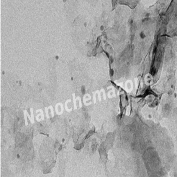
200mg Fluorinated Graphene Powder (Research Grade)

$505.00
Product 200mg Fluorinated Graphene Powder (Research Grade)
CAS No. 99685-96-8
Appearance Dark gray to black
Purity ≥99%,  ≥99.9%,  ≥95%(Other purities are also available)
APS 1–10µm (Size Can be customized),  Ask for other available size range.
Ingredient CₓFᵧ
Molecular Weight N/A
Melting Point N/A
Boiling Point N/A
Density 2.0–2.2 g/cm³
Product Codes NCZ-146I
 

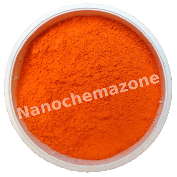
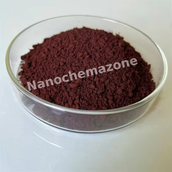
Lead (II, IV) Oxide (Pb3O4) 99.99% 4N Powder, 500g

$505.00
Product Lead (II, IV) Oxide (Pb3O4) 99.99% 4N Powder, 500g
CAS No. 1314-41-6
Appearance Bright red to orange-red crystalline
Purity ≥99%,  ≥99.9%,  ≥95%(Other purities are also available)
APS 1-10nm (Size Can be customized),  Ask for other available size range.
Ingredient Pb3O4
Molecular Weight 685.60 g/mol
Melting Point N/A
Boiling Point N/A
Density 8.3–9.1 g/cm³
Product Codes NCZ-443I

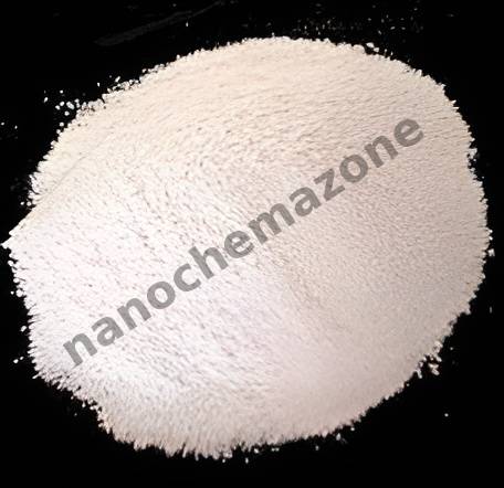
Aluminum Oxide (Al2O3) Sputtering Targets, Purity: 99.999%, Size: 1”, Thickness: 0.125”

$505.00

Product 

Aluminum Oxide (Al2O3) Sputtering Targets, Purity: 99.999%, Size: 1'', Thickness: 0.125''

CAS No.

 1344-28-1

Appearance

Powder

Purity

≥99%,  ≥99.9%,  ≥95%

(Other purities are also available)

APS

N/A (Size Can be customized), Ask for other available size ranges.

Ingredient

N/A

Molecular Weight

101.96 g/mol

Melting Point

~2,072 °C

Boiling Point

~2,977 °C

Density

~3.97–3.98 g/cm³

Product Codes

NCZ-2549K

β-Tricalcium phosphate(β-Ca3(PO4)2, >98%) (208982)

$505.00
Select options This product has multiple variants. The options may be chosen on the product page

Product 

β-Tricalcium phosphate(β-Ca3(PO4)2, >98%) (208982)

CAS No.

7758‑87‑4

Appearance

Powder

Purity

≥99%,  ≥99.9%,  ≥95%

(Other purities are also available)

APS

  <80um (Size Can be customized), Ask for other available size ranges.

Ingredient

N/A

Molecular Weight

~310.18 g/mol

Melting Point

~1670 °C

Boiling Point

N/A

Density

 β‑phase: ~3.066 g/cm³

Product Codes

NCZ-2611K

Aluminum Oxide (Al2O3) Sputtering Targets, Purity: 99.99%, Size: 3”, Thickness: 0.250”

$506.00

 Applications of Sputtering Targets;

Film deposition is accomplished using sputtering targets. A technique for sputtering thin films is called "deposition made by sputter targets," which entails eroding material from a "target" source onto a "substrate" like a silicon wafer. Etching of the target is done using semiconductor sputtering targets. When selectivity is not an issue and a high degree of etching anisotropy is required, sputter etching is the method of choice. By removing the target material through etching, sputter targets are also utilized for investigation. In secondary ion spectroscopy (SIMS), one example is when the target material is sputtered at a steady pace. When the target shatters,

Mass spectrometry measures the concentration and identity of sputtered atoms. The target material's composition may be ascertained and even very low concentrations of contaminants can be found with the aid of the sputtering target.

There is also an application area for sputtering targets in space. One type of space weathering that alters the chemical and physical characteristics of airless worlds like the Moon and asteroids is sputtering.

With the chemical formula Al2O3, aluminum oxide is a compound made of aluminum and oxygen.

Carbon (C) (Pyrolytic Graphite) Sputtering Targets, Purity: 99.999%, Size: 3”, Thickness: 0.250”

$506.00

Applications of Sputtering Targets;

Film deposition is accomplished using sputtering targets. A technique for sputtering thin films is called "deposition made by sputter targets," which entails eroding material from a "target" source onto a "substrate" like a silicon wafer. Etching of the target is done using semiconductor sputtering targets. When selectivity is not an issue and a high degree of etching anisotropy is required, sputter etching is the method of choice. By removing the target material through etching, sputter targets are also utilized for investigation. In secondary ion spectroscopy (SIMS), one example is when the target material is sputtered at a steady pace. Mass spectrometry is used to quantify the concentration and identity of spewed atoms as the target is sputtered.
The target material's composition may be ascertained and even very low concentrations of contaminants can be found with the aid of the sputtering target.

There is also an application area for sputtering targets in space. One type of space weathering that alters the chemical and physical characteristics of airless worlds like the Moon and asteroids is sputtering.

Molybdenum Disulfide (MoS2) Sputtering Targets, Purity: 99.9%, Size: 4”, Thickness: 0.250”

$506.00

Applications of Sputtering Targets;

Film deposition is accomplished using sputtering targets. A technique for sputtering thin films is called "deposition made by sputter targets," which entails eroding material from a "target" source onto a "substrate" like a silicon wafer. Etching of the target is done using semiconductor sputtering targets. When selectivity is not an issue and a high degree of etching anisotropy is required, sputter etching is the method of choice. By removing the target material through etching, sputter targets are also utilized for investigation. In secondary ion spectroscopy (SIMS), one example is when the target material is sputtered at a steady pace. Mass spectrometry is used to quantify the concentration and identity of spewed atoms as the target is sputtered.

By helping of the sputtering target, the composition of the target material may be evaluated and even extremely tiny amounts of contaminants are recognized.

There is also an application area for sputtering targets in space. One type of space weathering that alters the chemical and physical characteristics of airless worlds like the Moon and asteroids is sputtering.

Titanium Dioxide (TiO2) Sputtering Targets, indium, Purity: 99.9%, Size: 1”, Thickness: 0.125”, Grey to Black

$506.00

Applications of Sputtering Targets;

Film deposition is accomplished using sputtering targets. A technique for sputtering thin films is called "deposition made by sputter targets," which entails eroding material from a "target" source onto a "substrate" like a silicon wafer. Etching of the target is done using semiconductor sputtering targets. When selectivity is not an issue and a high degree of etching anisotropy is required, sputter etching is the method of choice. By removing the target material through etching, sputter targets are also utilized for investigation. In secondary ion spectroscopy (SIMS), one example is when the target material is sputtered at a steady pace. Mass spectrometry is used to quantify the concentration and identity of spewed atoms as the target is sputtered.

The target material's composition may be ascertained and even very low concentrations of contaminants can be found with the aid of the sputtering target.

There is also an application area for sputtering targets in space. One type of space weathering that alters the chemical and physical characteristics of airless worlds like the Moon and asteroids is sputtering.

Titanium Dioxide (TiO2) Sputtering Targets, Purity: 99.9%, Size: 3”, Thickness: 0.250”, Grey to Black

$506.00

Applications of Sputtering Targets;

Film deposition is accomplished using sputtering targets. A technique for sputtering thin films is called "deposition made by sputter targets," which entails eroding material from a "target" source onto a "substrate" like a silicon wafer. Etching of the target is done using semiconductor sputtering targets. When selectivity is not an issue and a high degree of etching anisotropy is required, sputter etching is the method of choice. By removing the target material through etching, sputter targets are also utilized for investigation. In secondary ion spectroscopy (SIMS), one example is when the target material is sputtered at a steady pace. Mass spectrometry is used to quantify the concentration and identity of spewed atoms as the target is sputtered.

The target material's composition may be ascertained and even very low concentrations of contaminants can be found with the aid of the sputtering target.

There is also an application area for sputtering targets in space. One type of space weathering that alters the chemical and physical characteristics of airless worlds like the Moon and asteroids is sputtering.

Tungsten Disulfide (WS2) Sputtering Targets, Purity: 99.9%, Size: 3”, Thickness: 0.250”

$506.00

Applications of Sputtering Targets;

Film deposition is accomplished using sputtering targets. A technique for sputtering thin films is called "deposition made by sputter targets," which entails eroding material from a "target" source onto a "substrate" like a silicon wafer. Etching of the target is done using semiconductor sputtering targets. When selectivity is not an issue and a high degree of etching anisotropy is required, sputter etching is the method of choice. By removing the target material through etching, sputter targets are also utilized for investigation. In secondary ion spectroscopy (SIMS), one example is when the target material is sputtered at a steady pace. Mass spectrometry is used to quantify the concentration and identity of spewed atoms as the target is sputtered.

The target material's composition may be ascertained and even very low concentrations of contaminants can be found with the aid of the sputtering target.

There is also an application area for sputtering targets in space. One type of space weathering that alters the chemical and physical characteristics of airless worlds like the Moon and asteroids is sputtering.

Zinc Oxide (ZnO) Sputtering Targets, Purity: 99.999%, Size: 2”, Thickness: 0.125”

$506.00

Applications of Sputtering Targets;

Film deposition is accomplished using sputtering targets. A technique for sputtering thin films is called "deposition made by sputter targets," which entails eroding material from a "target" source onto a "substrate" like a silicon wafer. Etching of the target is done using semiconductor sputtering targets. When selectivity is not an issue and a high degree of etching anisotropy is required, sputter etching is the method of choice. By removing the target material through etching, sputter targets are also utilized for investigation. In secondary ion spectroscopy (SIMS), one example is when the target material is sputtered at a steady pace. Mass spectrometry is used to quantify the concentration and identity of spewed atoms as the target is sputtered.

The target material's composition may be ascertained and even very low concentrations of contaminants can be found with the aid of the sputtering target.

There is also an application area for sputtering targets in space. One type of space weathering that alters the chemical and physical characteristics of airless worlds like the Moon and asteroids is sputtering.

High Purity Titanium Aluminum Carbide (Ti2AlC) MAX Phase Micron-Powder, 10g

Price range: $506.00 through $539.00
Select options This product has multiple variants. The options may be chosen on the product page
Product High Purity Titanium Aluminum Carbide (Ti2AlC) MAX Phase Micron-Powder, 10g
CAS No. 1446365-12-5
Appearance Gray to black fine
Purity ≥99%,  ≥99.9%,  ≥95%(Other purities are also available)
APS N/A
Ingredient Ti2AlC
Molecular Weight 171.78 g/mol
Melting Point N/A
Boiling Point N/A
Density 4.1 g/cm³
Product Codes NCZ-414I

Molybdenum Titanium Aluminum Carbide (Mo2Ti2AlC3) MAX Phase Micron-Powder, 5g

$506.00
Select options This product has multiple variants. The options may be chosen on the product page
Product Molybdenum Titanium Aluminum Carbide (Mo2Ti2AlC3) MAX Phase Micron-Powder, 5g
CAS No. 7783-40-6
Appearance Gray to black fine
Purity ≥99%,  ≥99.9%,  ≥95%(Other purities are also available)
APS 1 – 5µm (Size Can be customized),  Ask for other available size range.
Ingredient Mo2Ti2AlC3
Molecular Weight 408.49 g/mol
Melting Point 1400 °C
Boiling Point N/A
Density 5.0–6.0 g/cm³
Product Codes NCZ-452I
 

Monolayer Molybdenum Disulfide (MoS2) Nanopowder, Nano Flakes

Price range: $506.00 through $1,089.00
Select options This product has multiple variants. The options may be chosen on the product page
Product Monolayer Molybdenum Disulfide (MoS2) Nanopowder, Nano Flakes
CAS No. 1317-33-5
Appearance Black to dark gray
Purity ≥99%,  ≥99.9%,  ≥95%(Other purities are also available)
APS 100nm (Size Can be customized),  Ask for other available size range.
Ingredient MoS2
Molecular Weight 160.07 g/mol
Melting Point N/A
Boiling Point N/A
Density 5.06 g/cm³
Product Codes NCZ-457I

Indium Tin Oxide/ITO (In203:Sn02) Sputtering Targets, Purity: 99.99%, Size: 3”, Thickness: 0.125”

$506.00

Product 

Indium Tin Oxide/ITO (In203:Sn02) Sputtering Targets, Purity: 99.99%, Size: 3'', Thickness: 0.125''

CAS No.

• Indium Oxide (In₂O₃): 1312-43-2 • Tin Oxide (SnO₂): 18282-10-5

Appearance

Powder

Purity

≥99%,  ≥99.9%,  ≥95%

(Other purities are also available)

APS

< 5 µm (Size Can be customized), Ask for other available size ranges.

Ingredient

N/A

Molecular Weight

 Approx. 292.6 g/mol (based on 90:10 wt% In₂O₃:SnO₂ blend)

Melting Point

 ~1,800 °C (sintered ceramic composite; no sharp melting point)

Boiling Point

N/A

Density

 ~7.15 g/cm³

Product Codes

NCZ-2208K

Indium Tin Oxide/ITO (In203:Sn02) Sputtering Targets, Purity: 99.99%, Size: 1”, Thickness: 0.125”

$506.00

Product 

Indium Tin Oxide/ITO (In203:Sn02) Sputtering Targets, Purity: 99.99%, Size: 1'', Thickness: 0.125''

CAS No.

• Indium Oxide (In₂O₃): 1312-43-2 • Tin Oxide (SnO₂): 18282-10-5

Appearance

Powder

Purity

≥99%,  ≥99.9%,  ≥95%

(Other purities are also available)

APS

< 5 µm (Size Can be customized), Ask for other available size ranges.

Ingredient

N/A

Molecular Weight

 Approx. 292.6 g/mol (based on 90:10 wt% In₂O₃:SnO₂ blend)

Melting Point

 ~1,800 °C (sintered ceramic composite; no sharp melting point)

Boiling Point

N/A

Density

 ~7.15 g/cm³

Product Codes

NCZ-2212K

Titanium Nitride (TiN) Sputtering Targets, Purity: 99.5%, Size: 2”, Thickness: 0.125”

$507.00

Applications of Sputtering Targets;

Film deposition is accomplished using sputtering targets. A technique for sputtering thin films is called "deposition made by sputter targets," which entails eroding material from a "target" source onto a "substrate" like a silicon wafer. Etching of the target is done using semiconductor sputtering targets. When selectivity is not an issue and a high degree of etching anisotropy is required, sputter etching is the method of choice. By removing the target material through etching, sputter targets are also utilized for investigation. In secondary ion spectroscopy (SIMS), one example is when the target material is sputtered at a steady pace. Mass spectrometry is used to quantify the concentration and identity of spewed atoms as the target is sputtered.

The target material's composition may be ascertained and even very low concentrations of contaminants can be found with the aid of the sputtering target.

There is also an application area for sputtering targets in space. One type of space weathering that alters the chemical and physical characteristics of airless worlds like the Moon and asteroids is sputtering.

Tungsten Disulfide (WS2) Sputtering Targets, Purity: 99.9%, Size: 5”, Thickness: 0.250”

$507.00

Applications of Sputtering Targets;

Film deposition is accomplished using sputtering targets. A technique for sputtering thin films is called "deposition made by sputter targets," which entails eroding material from a "target" source onto a "substrate" like a silicon wafer. Etching of the target is done using semiconductor sputtering targets. When selectivity is not an issue and a high degree of etching anisotropy is required, sputter etching is the method of choice. By removing the target material through etching, sputter targets are also utilized for investigation. In secondary ion spectroscopy (SIMS), one example is when the target material is sputtered at a steady pace. Mass spectrometry is used to quantify the concentration and identity of spewed atoms as the target is sputtered.

The target material's composition may be ascertained and even very low concentrations of contaminants can be found with the aid of the sputtering target.

There is also an application area for sputtering targets in space. One type of space weathering that alters the chemical and physical characteristics of airless worlds like the Moon and asteroids is sputtering.