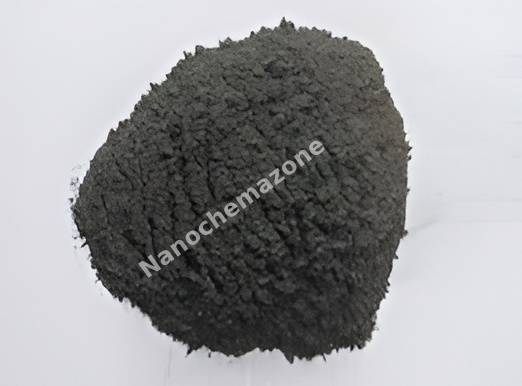
Titanium Nanoparticles/Nanopowder PVP Coated ( Ti, 99.9%, 40~60nm)

$480.00
Select options This product has multiple variants. The options may be chosen on the product page
$480/100g

Product 

Titanium Nanoparticles/Nanopowder PVP Coated ( Ti, 99.9%, 40~60nm)

CAS No.

7440-32-6

Appearance

Powder

Purity

≥99%,  ≥99.9%,  ≥95%

(Other purities are also available)

APS

40~60nm (Size Can be customized), Ask for other available size ranges.

Ingredient

N/A

Molecular Weight

47.87 g/mol

Melting Point

1,668 °C

Boiling Point

3,287 °C

Density

4.51 g/cm³

Product Codes

NCZ-1079K

Aluminum doped Zinc Oxide (AZO) Nanopowder 99.9% (3N), 100g

$480.00
Product Aluminum doped Zinc Oxide (AZO) Nanopowder 99.9% (3N), 100g
CAS No. 1314-13-2
Appearance Fine white
Purity ≥99%,  ≥99.9%,  ≥95%(Other purities are also available)
APS 20–80nm (Size Can be customized),  Ask for other available size range.
Ingredient (Zn₁₋ₓAlₓ)O
Molecular Weight 81.38 g/mol
Melting Point N/A
Boiling Point N/A
Density 5.6 g/cm³
Product Codes NCZ-278I
 

High Purified (>95 wt%) Large Surface Area Single-walled Carbon Nanotubes (Floating Catalyst Method), 1g

$480.00
Product High Purified (>95 wt%) Large Surface Area Single-walled Carbon Nanotubes (Floating Catalyst Method), 1g
CAS No. 308068-56-6
Appearance Black
Purity ≥99%,  ≥99.9%,  ≥95%(Other purities are also available)
APS 1–2 nm (Size Can be customized),  Ask for other available size range.
Ingredient C
Molecular Weight N/A
Melting Point N/A
Boiling Point N/A
Density 1.3–1.4 g/cm³
Product Codes NCZ-383I

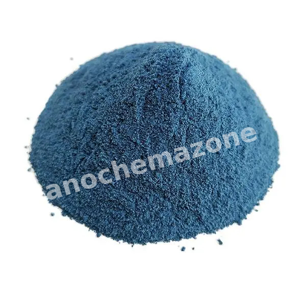
Indium Tin Oxide (ITO, 95:5wt%) Blue Nanopowder 99.99% (4N), 100g

$480.00
Product Indium Tin Oxide (ITO, 95:5wt%) Blue Nanopowder 99.99% (4N), 100g
CAS No. 1312-43-2
Appearance Blue
Purity ≥99%,  ≥99.9%,  ≥95%(Other purities are also available)
APS 20–50nm (Size Can be customized),  Ask for other available size range.
Ingredient In2−xSnxO
Molecular Weight 272–275 g/mol
Melting Point N/A
Boiling Point N/A
Density 7.14 g/cm³
Product Codes NCZ-427I
 

Lanthanum (III) Chloride Heptahydrate (LaCl3 · 7H2O) 99.99% 4N 500g

$480.00
Product Lanthanum (III) Chloride Heptahydrate (LaCl3 · 7H2O) 99.99% 4N 500g
CAS No. 10099-58-8
Appearance White crystalline powder or flaky crystals
Purity ≥99%,  ≥99.9%,  ≥95%(Other purifies are also available)
APS 100nm (Size Can be customized),  Ask for other available size range.
Ingredient LaCl3·7H2O
Molecular Weight N/A
Melting Point N/A
Boiling Point N/A
Density N/A
Product Codes NCZ-433I
 

Boron Nitride (BN) Sputtering Targets, Purity: 99.5%, Size: 3”, Thickness: 0.125”

$481.00

Applications of Sputtering Targets;

Film deposition is accomplished using sputtering targets. A technique for sputtering thin films is called "deposition made by sputter targets," which entails eroding material from a "target" source onto a "substrate" like a silicon wafer. Etching of the target is done using semiconductor sputtering targets. When selectivity is not an issue and a high degree of etching anisotropy is required, sputter etching is the method of choice. By removing the target material through etching, sputter targets are also utilized for investigation. In secondary ion spectroscopy (SIMS), one example is when the target material is sputtered at a steady pace. Mass spectrometry is used to quantify the concentration and identity of spewed atoms as the target is sputtered.

The target material's composition may be ascertained and even very low concentrations of contaminants can be found with the aid of the sputtering target.

There is also an application area for sputtering targets in space. One type of space weathering that alters the chemical and physical characteristics of airless worlds like the Moon and asteroids is sputtering.

Molybdenum Disulfide (MoS2) Sputtering Targets, Purity: 99.9%, Size: 2”, Thickness: 0.250”

$481.00

Applications of Sputtering Targets;

Film deposition is accomplished using sputtering targets. A technique for sputtering thin films is called "deposition made by sputter targets," which entails eroding material from a "target" source onto a "substrate" like a silicon wafer. Etching of the target is done using semiconductor sputtering targets. When selectivity is not an issue and a high degree of etching anisotropy is required, sputter etching is the method of choice. By removing the target material through etching, sputter targets are also utilized for investigation. In secondary ion spectroscopy (SIMS), one example is when the target material is sputtered at a steady pace. Mass spectrometry is used to quantify the concentration and identity of spewed atoms as the target is sputtered.

By helping of the sputtering target, the composition of the target material may be evaluated and even extremely tiny amounts of contaminants are recognized.

There is also an application area for sputtering targets in space. One type of space weathering that alters the chemical and physical characteristics of airless worlds like the Moon and asteroids is sputtering.

Zinc Oxide (ZnO) Sputtering Targets, Purity: 99.9%, Size: 3”, Thickness: 0.125”

$481.00

Applications of Sputtering Targets;

Film deposition is accomplished using sputtering targets. A technique for sputtering thin films is called "deposition made by sputter targets," which entails eroding material from a "target" source onto a "substrate" like a silicon wafer. Etching of the target is done using semiconductor sputtering targets. When selectivity is not an issue and a high degree of etching anisotropy is required, sputter etching is the method of choice. By removing the target material through etching, sputter targets are also utilized for investigation. In secondary ion spectroscopy (SIMS), one example is when the target material is sputtered at a steady pace. Mass spectrometry is used to quantify the concentration and identity of spewed atoms as the target is sputtered.

The target material's composition may be ascertained and even very low concentrations of contaminants can be found with the aid of the sputtering target.

There is also an application area for sputtering targets in space. One type of space weathering that alters the chemical and physical characteristics of airless worlds like the Moon and asteroids is sputtering.

Molybdenum Oxide (MoO3) Sputtering Targets, Purity: 99.9%, Size: 3”, Thickness: 0.250”

$481.00

Product 

Molybdenum Oxide (MoO3) Sputtering Targets, Purity: 99.9%, Size: 3'', Thickness: 0.250''

CAS No.

1313-27-5

Appearance

Powder

Purity

≥99%,  ≥99.9%,  ≥95%

(Other purities are also available)

APS

 N/A (Size Can be customized), Ask for other available size ranges.

Ingredient

N/A

Molecular Weight

 143.94 g/mol

Melting Point

 ~795°C

Boiling Point

 ~1155°C

Density

 ~4.7 g/cm³

Product Codes

NCZ-1900K

Silicon (Si) Sputtering Targets, N-type, Purity: 99.999%, Size: 6”, Thickness: 0.125”

$482.00

Product 

Silicon (Si) Sputtering Targets, N-type, Purity: 99.999%, Size: 6'', Thickness: 0.125''

CAS No.

7440-21-3

Appearance

Powder

Purity

≥99%,  ≥99.9%,  ≥95%

(Other purities are also available)

APS

N/A  (Size Can be customized), Ask for other available size ranges.

Ingredient

N/A

Molecular Weight

28.0855 g/mol

Melting Point

 1,414 °C

Boiling Point

3,265 °C

Density

 2.33 g/cm³

Product Codes

NCZ-1757K

Dicalcium silicate(Ca2SiO4) (205982)

$482.00
Select options This product has multiple variants. The options may be chosen on the product page

Product 

Dicalcium silicate(Ca2SiO4) (205982)

CAS No.

10034‑77‑2

Appearance

Powder

Purity

≥99%,  ≥99.9%,  ≥95%

(Other purities are also available)

APS

  <10um (Size Can be customized), Ask for other available size ranges.

Ingredient

N/A

Molecular Weight

~172.24 g/mol

Melting Point

~1540 °C (note: some sources mention up to 2130 °C for certain polymorphs)

Boiling Point

N/A

Density

 ~2.9 g/cm³

Product Codes

NCZ-2606K

Tricalcium silicate(Ca3SiO5) (203982)

$482.00
Select options This product has multiple variants. The options may be chosen on the product page

Product 

Tricalcium silicate(Ca3SiO5) (203982)

CAS No.

12168‑85‑3 — tricalcium silicate (also known as C₃S or alite)

Appearance

Powder

Purity

≥99%,  ≥99.9%,  ≥95%

(Other purities are also available)

APS

  <10um (Size Can be customized), Ask for other available size ranges.

Ingredient

N/A

Molecular Weight

~228.3 g/mol

Melting Point

~2150 °C — high-temperature data from CRC sources

Boiling Point

N/A

Density

 ~3.14 g/cm³

Product Codes

NCZ-2607K

Tristrontium silicate(Sr3SiO5) (203677)

$482.00
Select options This product has multiple variants. The options may be chosen on the product page

Product 

Tristrontium silicate(Sr3SiO5) (203677)

CAS No.

12712‑63‑9

Appearance

Powder

Purity

≥99%,  ≥99.9%,  ≥95%

(Other purities are also available)

APS

  <30um (Size Can be customized), Ask for other available size ranges.

Ingredient

N/A

Molecular Weight

N/A

Melting Point

N/A

Boiling Point

N/A

Density

~4.74 g/cm³ (as tristrontium silicate is termed Sr₃[SiO₄]O

Product Codes

NCZ-2608K

Tungsten Disulfide (WS2) Sputtering Targets, Purity: 99.9%, Size: 5”, Thickness: 0.125”

$484.00

Product 

Tungsten Disulfide (WS2) Sputtering Targets, Purity: 99.9%, Size: 5'', Thickness: 0.125''

CAS No.

 12138-09-9

Appearance

Powder

Purity

≥99%,  ≥99.9%,  ≥95%

(Other purities are also available)

APS

N/A  (Size Can be customized), Ask for other available size ranges.

Ingredient

N/A

Molecular Weight

247.97 g/mol

Melting Point

~1,250 °C

Boiling Point

N/A

Density

~7.5 g/cm³

Product Codes

NCZ-1578K

99.99% 30-80 nm Rutile Titanium Dioxide TiO2 Nanoparticles, 500g

$484.00
Product 99.99% 30-80 nm Rutile Titanium Dioxide TiO2 Nanoparticles, 500g
CAS No. 1317-80-2
Appearance White
Purity ≥99%,  ≥99.9%,  ≥95%(Other purities are also available)
APS 30-80nm  (Size Can be customized),  Ask for other available size range.
Ingredient TiO2
Molecular Weight N/A
Melting Point N/A
Boiling Point N/A
Density 0.5–0.8 g/cm³
Product Codes NCZ-234I
 

Imidazole-modified Graphene Quantum Dots Solution, 1mg/mL

$484.00
Select options This product has multiple variants. The options may be chosen on the product page
Product   Imidazole-modified Graphene Quantum Dots Solution, 1mg/mL
CAS No. N/A
Appearance Clear to pale yellow/brown
Purity ≥99%,  ≥99.9%,  ≥95%(Other purities are also available)
APS 2–10nm (Size Can be customized),  Ask for other available size range.
Ingredient CₓHᵧO_z
Molecular Weight N/A
Melting Point N/A
Boiling Point N/A
Density N/A
Product Codes NCZ-423I

Porous Graphene Powder, 20mg

$484.00
Product Porous Graphene Powder, 20mg
CAS No. 1034343-98-0
Appearance Black
Purity ≥99%,  ≥99.9%,  ≥95%(Other purities are also available)
APS 1–10µm (Size Can be customized),  Ask for other available size range.
Ingredient Cₓ
Molecular Weight N/A
Melting Point N/A
Boiling Point N/A
Density 0.1–0.5 g/cm³
Product Codes NCZ-496I
 

Cobalt Iron Boron (Co-Fe-B) Sputtering Targets, Purity: 99.9%, Size: 1”, Thickness: 0.125”

$484.00

Product 

Cobalt Iron Boron (Co-Fe-B) Sputtering Targets, Purity: 99.9%, Size: 1'', Thickness: 0.125''

CAS No.

N/A

Appearance

Powder

Purity

≥99%,  ≥99.9%,  ≥95%

(Other purities are also available)

APS

 N/A (Size Can be customized), Ask for other available size ranges.

Ingredient

N/A

Molecular Weight

 ~135.943 g/mol

Melting Point

N/A

Boiling Point

N/A

Density

0.986 g/cm³ (SAM — verify via COA due to low value)

Product Codes

NCZ-2281K

Cobalt (Co) Sputtering Targets, Purity: 99.95%, Size: 6”, Thickness: 0.125”

$484.00

Product 

Cobalt (Co) Sputtering Targets, Purity: 99.95%, Size: 6'', Thickness: 0.125''

CAS No.

7440‑48‑4

Appearance

Powder

Purity

≥99%,  ≥99.9%,  ≥95%

(Other purities are also available)

APS

 N/A (Size Can be customized), Ask for other available size ranges.

Ingredient

N/A

Molecular Weight

58.93 g/mol (cobalt atomic weight)

Melting Point

~1,495 °C

Boiling Point

~2,870–2,927 °C

Density

~8.9 g/cm³

Product Codes

NCZ-2288K

Chromium Oxide (Cr2O3) Sputtering Targets, Purity: 99.8%-99.9%, Size: 2”, Thickness: 0.250”

$484.00

Product 

Chromium Oxide (Cr2O3) Sputtering Targets, Purity: 99.8%-99.9%, Size: 2'', Thickness: 0.250''

CAS No.

1308-38-9

Appearance

Powder

Purity

≥99%,  ≥99.9%,  ≥95%

(Other purities are also available)

APS

 N/A (Size Can be customized), Ask for other available size ranges.

Ingredient

N/A

Molecular Weight

 151.99 g/mol

Melting Point

2,435 °C

Boiling Point

 ~3,000 °C (approximate; may decompose before boiling)

Density

5.21 g/cm³

Product Codes

NCZ-2303K

Chromium diboride(CrB2, 99%-99.9%, 300mesh) (752530 )

Price range: $484.00 through $575.00
Select options This product has multiple variants. The options may be chosen on the product page
Chromium diboride(CrB2, 99%-99.9%, 300mesh) (752530 )
Product Codes- NCZ-2696K

Tetratitanium heptoxide(Ti4O7, 99.9%) (537552)

$485.00
Select options This product has multiple variants. The options may be chosen on the product page
Tetratitanium heptoxide(Ti4O7, 99.9%) (537552)
Coating material Chemical formula Purity(%) Refractive index at 550nm Transparency range(nm) Melting point(°C) Density (g/cm3) Particle size(mm)
Titanium heptoxide Ti4O7 99.9 2.1-2.4 400-12000 1760 4.6 0.1-2 1-3
Product Codes- NCZ-2785K

Molybdenum Oxide (MoO3) Sputtering Targets, Purity: 99.9%, Size: 4”, Thickness: 0.250”

$486.00

Applications of Sputtering Targets;

Film deposition is accomplished using sputtering targets. A technique for sputtering thin films is called "deposition made by sputter targets," which entails eroding material from a "target" source onto a "substrate" like a silicon wafer. Etching of the target is done using semiconductor sputtering targets. When selectivity is not an issue and a high degree of etching anisotropy is required, sputter etching is the method of choice. By removing the target material through etching, sputter targets are also utilized for investigation. In secondary ion spectroscopy (SIMS), one example is when the target material is sputtered at a steady pace. Mass spectrometry is used to quantify the concentration and identity of spewed atoms as the target is sputtered.

The target material's composition may be ascertained and even very low concentrations of contaminants can be found with the aid of the sputtering target.

There is also an application area for sputtering targets in space. One type of space weathering that alters the chemical and physical characteristics of airless worlds like the Moon and asteroids is sputtering.

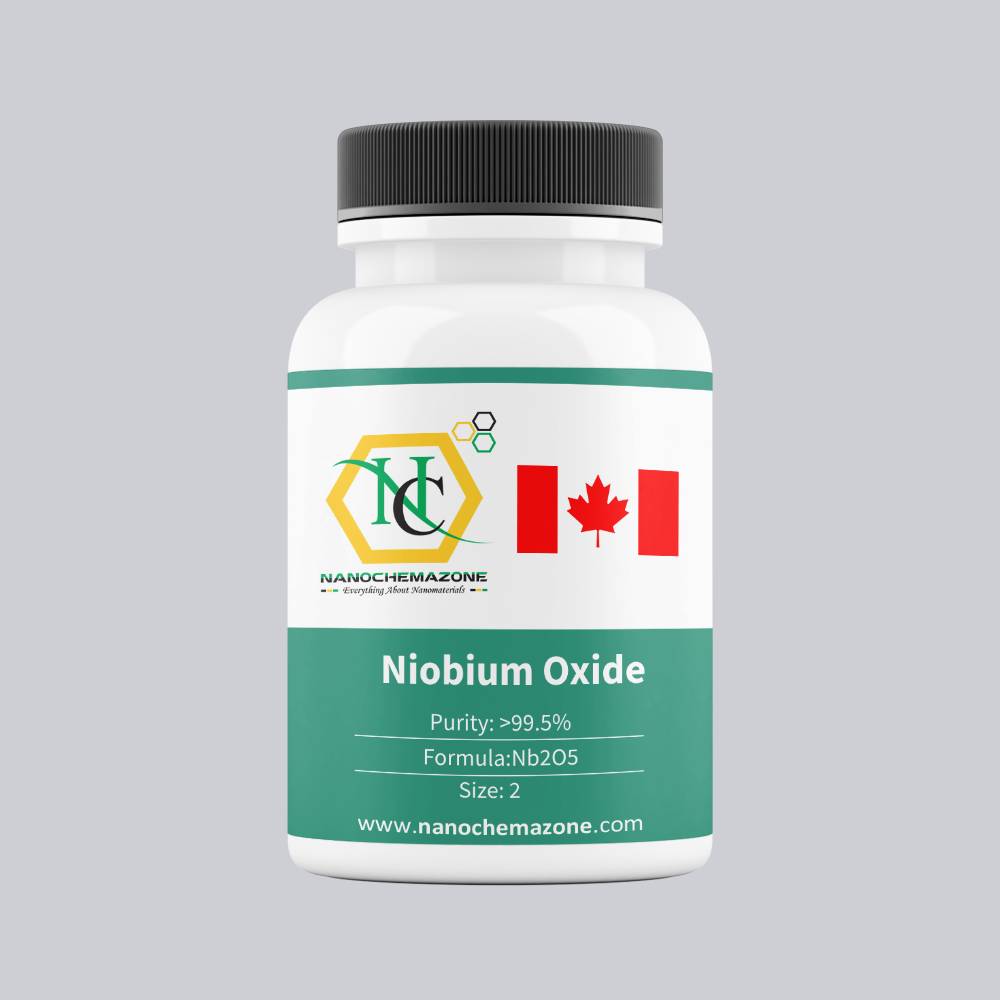
Niobium Oxide (Nb2O5) Sputtering Targets, indium, Purity: 99.5%, Size: 2”, Thickness: 0.125”

$486.00

Applications of Sputtering Targets;

Film deposition is accomplished using sputtering targets. A technique for sputtering thin films is called "deposition made by sputter targets," which entails eroding material from a "target" source onto a "substrate" like a silicon wafer. Etching of the target is done using semiconductor sputtering targets. When selectivity is not an issue and a high degree of etching anisotropy is required, sputter etching is the method of choice. By removing the target material through etching, sputter targets are also utilized for investigation. In secondary ion spectroscopy (SIMS), one example is when the target material is sputtered at a steady pace. Mass spectrometry is used to quantify the concentration and identity of spewed atoms as the target is sputtered.

The target material's composition may be ascertained and even very low concentrations of contaminants can be found with the aid of the sputtering target.

There is also an application area for sputtering targets in space. One type of space weathering that alters the chemical and physical characteristics of airless worlds like the Moon and asteroids is sputtering.

Niobium Oxide (Nb2O5) Sputtering Targets, indium, Purity: 99.5%, Size: 2”, Thickness: 0.125”

$486.00

Applications of Sputtering Targets;

Film deposition is accomplished using sputtering targets. A technique for sputtering thin films is called "deposition made by sputter targets," which entails eroding material from a "target" source onto a "substrate" like a silicon wafer. Etching of the target is done using semiconductor sputtering targets. When selectivity is not an issue and a high degree of etching anisotropy is required, sputter etching is the method of choice. By removing the target material through etching, sputter targets are also utilized for investigation. In secondary ion spectroscopy (SIMS), one example is when the target material is sputtered at a steady pace. Mass spectrometry is used to quantify the concentration and identity of spewed atoms as the target is sputtered.

The target material's composition may be ascertained and even very low concentrations of contaminants can be found with the aid of the sputtering target.

There is also an application area for sputtering targets in space. One type of space weathering that alters the chemical and physical characteristics of airless worlds like the Moon and asteroids is sputtering.

Silicon Nitride (Si3N4) Sputtering Targets, Purity: 99.9%, Size: 2”, Thickness: 0.125”, White to Gray

$486.00

Product 

Silicon Nitride (Si3N4) Sputtering Targets, Purity: 99.9%, Size: 2'', Thickness: 0.125'', White to Gray

CAS No.

 12033-89-5

Appearance

Powder

Purity

≥99%,  ≥99.9%,  ≥95%

(Other purities are also available)

APS

N/A  (Size Can be customized), Ask for other available size ranges.

Ingredient

N/A

Molecular Weight

 140.28 g/mol

Melting Point

 ~1900 °C

Boiling Point

N/A

Density

~3.2 g/cm³

Product Codes

NCZ-1700K

Silicon (Si) Sputtering Targets, N-type, Purity: 99.999%, Size: 5”, Thickness: 0.250”

$486.00

Product 

Silicon (Si) Sputtering Targets, N-type, Purity: 99.999%, Size: 5'', Thickness: 0.250''

CAS No.

7440-21-3

Appearance

Powder

Purity

≥99%,  ≥99.9%,  ≥95%

(Other purities are also available)

APS

N/A  (Size Can be customized), Ask for other available size ranges.

Ingredient

N/A

Molecular Weight

28.0855 g/mol

Melting Point

 1,414 °C

Boiling Point

3,265 °C

Density

 2.33 g/cm³

Product Codes

NCZ-1758K

Ytterbium Oxide (Yb2O3) Sputtering Targets, Purity: 99.99%, Size: 1”, Thickness: 0.250”

$487.00

Applications of Sputtering Targets;

Film deposition is accomplished using sputtering targets. A technique for sputtering thin films is called "deposition made by sputter targets," which entails eroding material from a "target" source onto a "substrate" like a silicon wafer. Etching of the target is done using semiconductor sputtering targets. When selectivity is not an issue and a high degree of etching anisotropy is required, sputter etching is the method of choice. By removing the target material through etching, sputter targets are also utilized for investigation. In secondary ion spectroscopy (SIMS), one example is when the target material is sputtered at a steady pace. Mass spectrometry is used to quantify the concentration and identity of spewed atoms as the target is sputtered.

The target material's composition may be ascertained and even very low concentrations of contaminants can be found with the aid of the sputtering target.

There is also an application area for sputtering targets in space. One type of space weathering that alters the chemical and physical characteristics of airless worlds like the Moon and asteroids is sputtering.

Antimony (Sb) Sputtering Targets, indium, Purity: 99.999%, Size: 1”, Thickness: 0.125”

$487.00

Product 

Antimony (Sb) Sputtering Targets, indium, Purity: 99.999%, Size: 1'', Thickness: 0.125''

CAS No.

 7440-36-0

Appearance

Powder

Purity

≥99%,  ≥99.9%,  ≥95%

(Other purities are also available)

APS

N/A (Size Can be customized), Ask for other available size ranges.

Ingredient

N/A

Molecular Weight

 121.76 g/mol

Melting Point

 630.6 °C

Boiling Point

 1587 °C

Density

 6.69 g/cm³

Product Codes

NCZ-2504K

Vanadium Oxide (V2O5) Sputtering Targets, Purity: 99.9%, Size: 1”, Thickness: 0.250”

$488.00

Product 

Vanadium Oxide (V2O5) Sputtering Targets, Purity: 99.9%, Size: 1'', Thickness: 0.250''

CAS No.

1314‑62‑1

Appearance

Powder

Purity

≥99%,  ≥99.9%,  ≥95%

(Other purities are also available)

APS

N/A  (Size Can be customized), Ask for other available size ranges.

Ingredient

N/A

Molecular Weight

181.88 g/mol

Melting Point

690 °C

Boiling Point

~1750 °C

Density

~3.35 g/cm³

Product Codes

NCZ-1541K

Silicon Carbide (SiC) Sputtering Targets, Purity: 99.5%, Size: 1”, Thickness: 0.250”

$488.00

Product 

Silicon Carbide (SiC) Sputtering Targets, Purity: 99.5%, Size: 1'', Thickness: 0.250''

CAS No.

 409-21-2

Appearance

Powder

Purity

≥99%,  ≥99.9%,  ≥95%

(Other purities are also available)

APS

N/A  (Size Can be customized), Ask for other available size ranges.

Ingredient

N/A

Molecular Weight

 40.10 g/mol

Melting Point

~2,700 °C

Boiling Point

N/A

Density

~3.21 g/cm³

Product Codes

NCZ-1729K

Silicon (Si) Sputtering Targets, P-type, Purity: 99.999%, Size: 6”, Thickness: 0.250”

$488.00

Product 

Silicon (Si) Sputtering Targets, P-type, Purity: 99.999%, Size: 6'', Thickness: 0.250''

CAS No.

7440-21-3

Appearance

Powder

Purity

≥99%,  ≥99.9%,  ≥95%

(Other purities are also available)

APS

N/A  (Size Can be customized), Ask for other available size ranges.

Ingredient

N/A

Molecular Weight

28.0855 g/mol

Melting Point

 1,414 °C

Boiling Point

3,265 °C

Density

 2.33 g/cm³

Product Codes

NCZ-1744K

Nickel (Ni) Sputtering Targets, Purity: 99.995%, Size: 6”, Thickness: 0.125”

$488.00

Product 

Nickel (Ni) Sputtering Targets, Purity: 99.995%, Size: 6'', Thickness: 0.125''

CAS No.

7440-02-0

Appearance

Powder

Purity

≥99%,  ≥99.9%,  ≥95%

(Other purities are also available)

APS

 N/A (Size Can be customized), Ask for other available size ranges.

Ingredient

N/A

Molecular Weight

 58.69 g/mol

Melting Point

 1,455 °C

Boiling Point

 2,732 °C

Density

 8.90 g/cm³

Product Codes

NCZ-1871K

Lanthanum Strontium Manganate (La0.9Sr0.1MnO3) Sputtering Targets, Purity: 99.9%, Size: 2”, Thickness: 0.125”

$488.00

Product 

Lanthanum Strontium Manganate (La0.9Sr0.1MnO3) Sputtering Targets, Purity: 99.9%, Size: 2'', Thickness: 0.125''

CAS No.

 ~68189‑52‑4 (generic for La₁₋ₓSrₓMnO₃ perovskites)

Appearance

Powder

Purity

≥99%,  ≥99.9%,  ≥95%

(Other purities are also available)

APS

<5 µm (Size Can be customized), Ask for other available size ranges.

Ingredient

N/A

Molecular Weight

 ~ 237.5 g/mol (based on La, Sr, Mn, and O content)

Melting Point

 > 300 °C (decomposes before melting)

Boiling Point

N/A

Density

 ~ 6.4 g/cm³ crystallographic density (typical for La₀.₉Sr₀.₁MnO₃ perovskite)

Product Codes

NCZ-2098K

Chromium (Cr) Sputtering Targets, Purity: 99.95%, Size: 4”, Thickness: 0.250”

$488.00

Product 

Chromium (Cr) Sputtering Targets, Purity: 99.95%, Size: 4'', Thickness: 0.250''

CAS No.

7440‑47‑3

Appearance

Powder

Purity

≥99%,  ≥99.9%,  ≥95%

(Other purities are also available)

APS

 N/A (Size Can be customized), Ask for other available size ranges.

Ingredient

N/A

Molecular Weight

 51.9961 g/mol

Melting Point

 1,857 °C

Boiling Point

 2,672 °C

Density

 7.14 g/cm³

Product Codes

NCZ-2312K

Silver Nanowires Suspension in Ethanol, Purity: > 99 wt%, Diameter : 50 nm

Price range: $490.00 through $8,590.00
Select options This product has multiple variants. The options may be chosen on the product page

Applications:

Recently, the usage areas of silver nanowires are  listed as;

Air and water purification Antimicrobial applications (e.g., bandages, coatings for medical devices, antibacterial fabrics) Catalysts Compact logic gates E-paper EMI shielding films and paints Fillers for high performance conductive adhesives Flexible antennas Flexible displays Light-emitting diodes (LEDs), OLED devices, OLED lighting Liquid crystal displays Medical imaging Optical limiters Sensors and detectors Solar cells, solar panels, thin film photovoltaics Surface enhanced spectroscopy (SERS) Touch screens for smartphones, tablets, and wearable electronics Waveguides

Lanthanum Titanate (LaTiO3) Sputtering Targets, Purity: 99.9%, Size: 1”, Thickness: 0.250”

$490.00

Applications of Sputtering Targets;

  • Sputtering targets is used for film deposition. The deposition made by sputter targets is a method of depositing thin films by sputtering that involves eroding material from a "target" source onto a "substrate" such as  a silicon wafer.
  • Semiconductor sputtering targets is used to etch the target. Sputter etching is chosen in cases where a high degree of etching anisotropy is needed and selectivity is not a concern.
  • Sputter targets is also used for analysis by etching away the target material.
One of the example occurs in secondary ion spectroscopy (SIMS), where the target sample is sputtered at a constant rate. As the target is sputtered, the concentration and identity of sputtered atoms are measured using mass spectrometry. By helping of the sputtering target, the composition of the target material can be determined and even extremely low concentrations of impurities are detected. Sputtering target has also application area in space. Sputtering is one of the forms of space weathering, a process that changes the physical and chemical properties of airless bodies, such as asteroids and the Moon.

Zinc Sulfide (ZnS) Sputtering Targets, Purity: 99.99%, Size: 2”, Thickness: 0.250”

$490.00

Applications of Sputtering Targets;

Film deposition is accomplished using sputtering targets. A technique for sputtering thin films is called "deposition made by sputter targets," which entails eroding material from a "target" source onto a "substrate" like a silicon wafer. Etching of the target is done using semiconductor sputtering targets. When selectivity is not an issue and a high degree of etching anisotropy is required, sputter etching is the method of choice. By removing the target material through etching, sputter targets are also utilized for investigation. In secondary ion spectroscopy (SIMS), one example is when the target material is sputtered at a steady pace. Mass spectrometry is used to quantify the concentration and identity of spewed atoms as the target is sputtered.

The target material's composition may be ascertained and even very low concentrations of contaminants can be found with the aid of the sputtering target.

There is also an application area for sputtering targets in space. One type of space weathering that alters the chemical and physical characteristics of airless worlds like the Moon and asteroids is sputtering.

Permalloy (Ni-Fe-Mo) Sputtering Targets, Size: 4”, Thickness: 0.250”

$490.00

Product 

Permalloy (Ni-Fe-Mo) Sputtering Targets, Size: 4'', Thickness: 0.250''

CAS No.

 Nickel: 7440-02-0 Iron: 7439-89-6 Molybdenum: 7439-98-7

Appearance

Powder

Purity

≥99%,  ≥99.9%,  ≥95%

(Other purities are also available)

APS

N/A (Size Can be customized), Ask for other available size ranges.

Ingredient

N/A

Molecular Weight

 Not defined (alloy), but elemental weights: Ni: 58.69 g/mol Fe: 55.85 g/mol Mo: 95.95 g/mol

Melting Point

 ~1450 °C

Boiling Point

 ~2730–3000 °C

Density

~8.7 g/cm³

Product Codes

NCZ-1796K

Indium (In) Sputtering Targets, Purity: 99.99%, Size: 3”, Thickness: 0.250”

$490.00

Product 

Indium (In) Sputtering Targets, Purity: 99.99%, Size: 3'', Thickness: 0.250''

CAS No.

 7440-74-6

Appearance

Powder

Purity

≥99%,  ≥99.9%,  ≥95%

(Other purities are also available)

APS

 N/A (Size Can be customized), Ask for other available size ranges.

Ingredient

N/A

Molecular Weight

114.82 g/mol

Melting Point

 156.6 °C

Boiling Point

 2,072 °C

Density

 7.31 g/cm³

Product Codes

NCZ-2225K

Carbon (C) (Pyrolytic Graphite) Sputtering Targets, Purity: 99.999%, Size: 4”, Thickness: 0.125”

$490.00

Product 

Carbon (C) (Pyrolytic Graphite) Sputtering Targets, Purity: 99.999%, Size: 4'', Thickness: 0.125''

CAS No.

 7782-42-5

Appearance

Powder

Purity

≥99%,  ≥99.9%,  ≥95%

(Other purities are also available)

APS

 N/A (Size Can be customized), Ask for other available size ranges.

Ingredient

N/A

Molecular Weight

 12.01 g/mol

Melting Point

Sublimes ~3652 °C (no true melting)

Boiling Point

Sublimes directly ~4,200°C

Density

 ~2.2–2.25 g/cm³

Product Codes

NCZ-2338K

Boron (B) Sputtering Targets, Purity: 99.9%, Size: 3”, Thickness: 0.250”

$491.00

Applications of Sputtering Targets;

Film deposition is accomplished using sputtering targets. A technique for sputtering thin films is called "deposition made by sputter targets," which entails eroding material from a "target" source onto a "substrate" like a silicon wafer. Etching of the target is done using semiconductor sputtering targets. When selectivity is not an issue and a high degree of etching anisotropy is required, sputter etching is the method of choice. By removing the target material through etching, sputter targets are also utilized for investigation. In secondary ion spectroscopy (SIMS), one example is when the target material is sputtered at a steady pace. Mass spectrometry is used to quantify the concentration and identity of spewed atoms as the target is sputtered.

The target material's composition may be ascertained and even very low concentrations of contaminants can be found with the aid of the sputtering target.

There is also an application area for sputtering targets in space. One type of space weathering that alters the chemical and physical characteristics of airless worlds like the Moon and asteroids is sputtering.

Iron Oxide (Fe3O4) Sputtering Targets, Purity: 99.9%, Size: 1”, Thickness: 0.125”

$491.00

Product 

Iron Oxide (Fe3O4) Sputtering Targets, Purity: 99.9%, Size: 1'', Thickness: 0.125''

CAS No.

1317‑61‑9

Appearance

Powder

Purity

≥99%,  ≥99.9%,  ≥95%

(Other purities are also available)

APS

 N/A (Size Can be customized), Ask for other available size ranges.

Ingredient

N/A

Molecular Weight

 231.6 g/mol

Melting Point

~1,597 °C

Boiling Point

 ~2,623 °C (material may decompose before boiling)

Density

 ~5.17 g/cm³ (sintered target)

Product Codes

NCZ-2177K

Surface Functionalized Superparamagnetic Iron Oxide Nanoparticle (SPION) High Concentration Suspension

Price range: $491.00 through $1,525.00
Select options This product has multiple variants. The options may be chosen on the product page
Product Surface Functionalized Superparamagnetic Iron Oxide Nanoparticle (SPION) High Concentration Suspension
CAS No. 1317-61-9
Appearance Dark brown to black
Purity ≥99%,  ≥99.9%,  ≥95%(Other purities are also available)
APS 12nm (Size Can be customized),  Ask for other available size range.
Ingredient Fe3O4-X
Molecular Weight N/A
Melting Point N/A
Boiling Point N/A
Density N/A
Product Codes NCZ-546I

Cobalt Iron Boron (Co-Fe-B) Sputtering Targets, Purity: 99.9%, Size: 2”, Thickness: 0.250”

$492.00

Applications of Sputtering Targets;

Film deposition is accomplished using sputtering targets. A technique for sputtering thin films is called "deposition made by sputter targets," which entails eroding material from a "target" source onto a "substrate" like a silicon wafer. Etching of the target is done using semiconductor sputtering targets. When selectivity is not an issue and a high degree of etching anisotropy is required, sputter etching is the method of choice. By removing the target material through etching, sputter targets are also utilized for investigation. In secondary ion spectroscopy (SIMS), one example is when the target material is sputtered at a steady pace. Mass spectrometry is used to quantify the concentration and identity of spewed atoms as the target is sputtered.

The target material's composition may be ascertained and even very low concentrations of contaminants can be found with the aid of the sputtering target.

There is also an application area for sputtering targets in space. One type of space weathering that alters the chemical and physical characteristics of airless worlds like the Moon and asteroids is sputtering.

An alloy consisting of cobalt, iron, and boron can be utilized as a sputtering target. Let's examine the possible uses for cobalt, iron, and boron alloys.

Indium Oxide (In2O3) Sputtering Targets, Purity: 99.99%, Size: 2”, Thickness: 0.250”

$492.00

Applications of Sputtering Targets;

Film deposition is accomplished using sputtering targets. A technique for sputtering thin films is called "deposition made by sputter targets," which entails eroding material from a "target" source onto a "substrate" like a silicon wafer. Etching of the target is done using semiconductor sputtering targets. When selectivity is not an issue and a high degree of etching anisotropy is required, sputter etching is the method of choice. By removing the target material through etching, sputter targets are also utilized for investigation. In secondary ion spectroscopy (SIMS), one example is when the target material is sputtered at a steady pace. Mass spectrometry is used to quantify the concentration and identity of spewed atoms as the target is sputtered.

The target material's composition may be ascertained and even very low concentrations of contaminants can be found with the aid of the sputtering target.

There is also an application area for sputtering targets in space. One type of space weathering that alters the chemical and physical characteristics of airless worlds like the Moon and asteroids is sputtering.

Magnesium (Mg) Sputtering Targets, Purity: 99.95%, Size: 8”, Thickness: 0.250”

$492.00

Applications of Sputtering Targets;

Film deposition is accomplished using sputtering targets. A technique for sputtering thin films is called "deposition made by sputter targets," which entails eroding material from a "target" source onto a "substrate" like a silicon wafer. Etching of the target is done using semiconductor sputtering targets. When selectivity is not an issue and a high degree of etching anisotropy is required, sputter etching is the method of choice. By removing the target material through etching, sputter targets are also utilized for investigation. In secondary ion spectroscopy (SIMS), one example is when the target material is sputtered at a steady pace. Mass spectrometry is used to quantify the concentration and identity of spewed atoms as the target is sputtered.

By helping of the sputtering target, the composition of the target material may be evaluated and even extremely tiny amounts of contaminants are recognized.

There is also an application area for sputtering targets in space. One type of space weathering that alters the chemical and physical characteristics of airless worlds like the Moon and asteroids is sputtering.

Nickel (Ni) Sputtering Targets, Purity: 99.995%, Size: 8”, Thickness: 0.250”

$493.00

Applications of Sputtering Targets;

Film deposition is accomplished using sputtering targets. A technique for sputtering thin films is called "deposition made by sputter targets," which entails eroding material from a "target" source onto a "substrate" like a silicon wafer. Etching of the target is done using semiconductor sputtering targets. When selectivity is not an issue and a high degree of etching anisotropy is required, sputter etching is the method of choice. By removing the target material through etching, sputter targets are also utilized for investigation. In secondary ion spectroscopy (SIMS), one example is when the target material is sputtered at a steady pace. Mass spectrometry is used to quantify the concentration and identity of spewed atoms as the target is sputtered.

The target material's composition may be ascertained and even very low concentrations of contaminants can be found with the aid of the sputtering target.

There is also an application area for sputtering targets in space. One type of space weathering that alters the chemical and physical characteristics of airless worlds like the Moon and asteroids is sputtering.

Nickel Vanadium (NiV) Sputtering Targets, Purity: 99.95%, Size: 6”, Thickness: 0.250”

$493.00

Product 

Nickel Vanadium (NiV) Sputtering Targets, Purity: 99.95%, Size: 6'', Thickness: 0.250''

CAS No.

11137-91-4

Appearance

Powder

Purity

≥99%,  ≥99.9%,  ≥95%

(Other purities are also available)

APS

N/A (Size Can be customized), Ask for other available size ranges.

Ingredient

N/A

Molecular Weight

~57.9 g/mol

Melting Point

~1,350–1,450 °C

Boiling Point

N/A

Density

 ~8.5 g/cm³

Product Codes

NCZ-1822K

Lanthanum Calcium Manganate (La0.7Ca0.3MnO3) Sputtering Targets, Purity: 99.9%, Size: 3”, Thickness: 0.250”

$493.00

Product 

Lanthanum Calcium Manganate (La0.7Ca0.3MnO3) Sputtering Targets, Purity: 99.9%, Size: 3'', Thickness: 0.250''

CAS No.

123273‑09‑6

Appearance

Powder

Purity

≥99%,  ≥99.9%,  ≥95%

(Other purities are also available)

APS

 ~1–5 µm (Size Can be customized), Ask for other available size ranges.

Ingredient

N/A

Molecular Weight

 ~313.9 g/mol

Melting Point

 ~1,550 °C (approximate; ceramic decomposition likely above)

Boiling Point

N/A

Density

 ~5.3 g/cm³ @ room temp

Product Codes

NCZ-2153K

Carbon Nanotube Sponges, Size: 50 mm x 10 mm, Thickness: 3-4 mm

Price range: $494.00 through $2,139.00
Select options This product has multiple variants. The options may be chosen on the product page
Carbon Nanotube Sponges, Size: 50 mm x 10 mm, Thickness: 3-4 mm The carbon nanotube sponge structure is uniform and they possess good mechanical strength, good flexibility, high porosity and low density. They can be used as a purifying agent in order to absorb pollutants. These pollutants can be fertilizers, pesticides or pharmaceuticals found in water, energy storage materials, catalyst carriers or in high-efficiency composite materials.

Indium Phosphide (InP) Wafers, Size: 3”, Thickness: 600± 25 μm, Orientation: 111, Single Side Polished, Testing Grade

Price range: $494.00 through $2,320.00
Select options This product has multiple variants. The options may be chosen on the product page
1 piece/445  5 pieces/2090                            Please contact us for quotes on larger quantities !!!

Indium Phosphide (InP) Wafers

Size: 3'', Thickness: 600±25 μm, Orientation: 111

Technical Properties:

Size (inch)  3”
Thickness (μm)  600± 25
Dopant  Sulphur (N type)
Polished  Single Side
Mobility (1.5-3.5)E3
Orientation  111
EPD  ≤5000
Growth method  VGF
OF Length  22±2
IF Length   11±1

Fields of Application for Indium Phosphide (InP)

Indium phosphide (InP) is a binary semiconductor composed of indium and phosphorus. Indium phosphide (InP) has started to be developed at the beginning of 1980s. Indium phosphide (InP) which used in a high power and high frequency electronics, has superior electron velocity. Indium phosphide (InP) has a direct bandgap by contrast with many semiconductors. This makes indium phosphide (InP) useful for optoelectronics and laser diodes. Indium phosphide (InP) is a crucial material for production of laser signals, determination and conversion of those signals back to electronic form. Indium Phopshide (InP) is a binary semiconductor composed of Indium (In) and Phosphorus (P), belonging to a group of materials commonly known as III-V Semiconductors. InP is used in high power and high-frequency electronics and boasts a superior electron velocity in comparison to more common semiconductors such as Silicon and Gallium Arsenide. Indium Phosphide has a face-centred cubic crystal structure almost identical to that of GaAs and most of the lll-V semiconductors. InP wafers must be prepared prior to device fabrication, all III-V wafers must be lapped to remove surface damage that occurs during the slicing process. Wafers are then Chemically Mechanically Polished/Plaranrized (CMP) for the final material removal stage allowing for the attainment of super-flat mirror like surfaces with a remaining roughness on an atomic scale. The wafer is then ready for device fabrication.
  • Indium phosphide (InP) is used in modulators.
  • Indium phosphide (InP) is used in photo-detectors.
  • Indium phosphide (InP) is used in LEDs.
  • Indium phosphide (InP) is used in fiber communications components.
  • Indium phosphide (InP) is used in semiconductor optical amplifiers.

Indium Phosphide (InP) Wafers, Size: 3”, Thickness: 600± 25 μm, Orientation: 100, Single Side Polished, Testing Grade

Price range: $494.00 through $2,320.00
Select options This product has multiple variants. The options may be chosen on the product page
1 piece/445  5 pieces/2090                            Please contact us for quotes on larger quantities !!!

Indium Phosphide (InP) Wafers

Size: 3'', Thickness: 600±25 μm, Orientation: 100

Technical Properties:

Size (inch)  3”
Thickness (μm)  600± 25
Dopant  Sulphur (N type)
Polished  Single Side
Mobility (1.5-3.5)E3
Orientation  100
EPD  ≤5000
Growth method  VGF
OF Length  22±2
IF Length   11±1

Fields of Application for Indium Phosphide (InP)

Indium phosphide (InP) is a binary semiconductor composed of indium and phosphorus. Indium phosphide (InP) has started to be developed at the beginning of 1980s. Indium phosphide (InP) which used in a high power and high frequency electronics, has superior electron velocity. Indium phosphide (InP) has a direct bandgap by contrast with many semiconductors. This makes indium phosphide (InP) useful for optoelectronics and laser diodes. Indium phosphide (InP) is a crucial material for production of laser signals, determination and conversion of those signals back to electronic form. Indium Phopshide (InP) is a binary semiconductor composed of Indium (In) and Phosphorus (P), belonging to a group of materials commonly known as III-V Semiconductors. InP is used in high power and high-frequency electronics and boasts a superior electron velocity in comparison to more common semiconductors such as Silicon and Gallium Arsenide. Indium Phosphide has a face-centred cubic crystal structure almost identical to that of GaAs and most of the lll-V semiconductors. InP wafers must be prepared prior to device fabrication, all III-V wafers must be lapped to remove surface damage that occurs during the slicing process. Wafers are then Chemically Mechanically Polished/Plaranrized (CMP) for the final material removal stage allowing for the attainment of super-flat mirror like surfaces with a remaining roughness on an atomic scale. The wafer is then ready for device fabrication.
  • Indium phosphide (InP) is used in modulators.
  • Indium phosphide (InP) is used in photo-detectors.
  • Indium phosphide (InP) is used in LEDs.
  • Indium phosphide (InP) is used in fiber communications components.
  • Indium phosphide (InP) is used in semiconductor optical amplifiers.

High-Performance Copper Foil Rolls for Lithium Ion Battery, Size: 10 µm

Price range: $494.00 through $2,175.00
Select options This product has multiple variants. The options may be chosen on the product page
1 roll/494 € 5 rolls/2175 € Please contact us for quotes on larger quantities !!! High-Performance Copper Foil Rolls for Lithium Ion Battery

High-Performance Copper Foil Rolls for Lithium Ion Battery, Size: 10 µm

Price range: $494.00 through $2,175.00
Select options This product has multiple variants. The options may be chosen on the product page
1 roll/494 € 5 rolls/2175 € Please contact us for quotes on larger quantities !!! High-Performance Copper Foil Rolls for Lithium Ion Battery

Vanadium (V) Sputtering Targets, Purity: 99.5%, Size: 4”, Thickness: 0.125”

$494.00

Product 

Vanadium (V) Sputtering Targets, Purity: 99.5%, Size: 4'', Thickness: 0.125''

CAS No.

7440-62-2

Appearance

Powder

Purity

≥99%,  ≥99.9%,  ≥95%

(Other purities are also available)

APS

N/A  (Size Can be customized), Ask for other available size ranges.

Ingredient

N/A

Molecular Weight

50.9415 g/mol

Melting Point

1910 °C

Boiling Point

3407 °C

Density

6.11 g/cm³

Product Codes

NCZ-1546K

Antimony (Sb) Sputtering Targets, Purity: 99.999%, Size: 3”, Thickness: 0.250”

$494.00

Product 

Antimony (Sb) Sputtering Targets, Purity: 99.999%, Size: 3'', Thickness: 0.250''

CAS No.

 7440-36-0

Appearance

Powder

Purity

≥99%,  ≥99.9%,  ≥95%

(Other purities are also available)

APS

N/A (Size Can be customized), Ask for other available size ranges.

Ingredient

N/A

Molecular Weight

 121.76 g/mol

Melting Point

 630.6 °C

Boiling Point

 1587 °C

Density

 6.69 g/cm³

Product Codes

NCZ-2505K

Shape Memory Polymer NGM2520, Ether Type

Price range: $495.00 through $6,175.00
Select options This product has multiple variants. The options may be chosen on the product page

Applications:

Shape Memory Polymer (SMP) has myriad of advanced applications in different fields from daily life uses like textile to biomedicals. These applications include smart catheter, drug-delivery systems, biosensors, auto-repairing automobile parts, smart textile, self-healing materials, smart suture, artificial organs like muscles, and so on.

Meshed Lithium Air CR2032 Coin Cell Case with 304SS, Diameter: 20 mm, Height: 3.2 mm

Price range: $495.00 through $1,571.00
Select options This product has multiple variants. The options may be chosen on the product page

Applications:

Meshed Lithium Air CR2032 Coin Cell Case with 304SS is widely used for developing Zinc/Lithium Air battery.

Hydrothermal Synthesis Autoclave Reactor with PPL Lined Vessel 500 ml

Price range: $495.00 through $2,215.00
Select options This product has multiple variants. The options may be chosen on the product page
APPLICATIONs
  • Chemical synthesis
  • Synthesizing of nanoparticles
  • For cultured crystal growth
  • Polymerization reaction
  • Hydrothermal decomposition
  • Catalyst synthesis
  • Hydrothermal oxidation
  • Hydrothermal precipitation
  • Material Digester / digestion
  • Crystallization process
  • Dissolve of heavy metals, refractory material, organic chemicals etc.