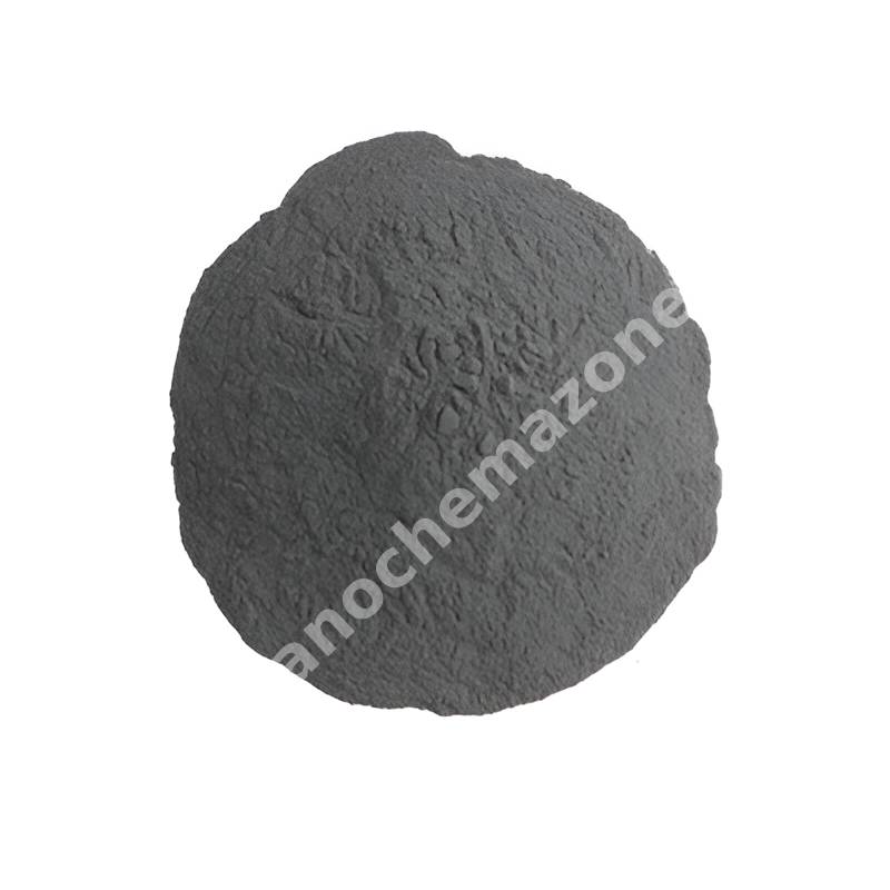
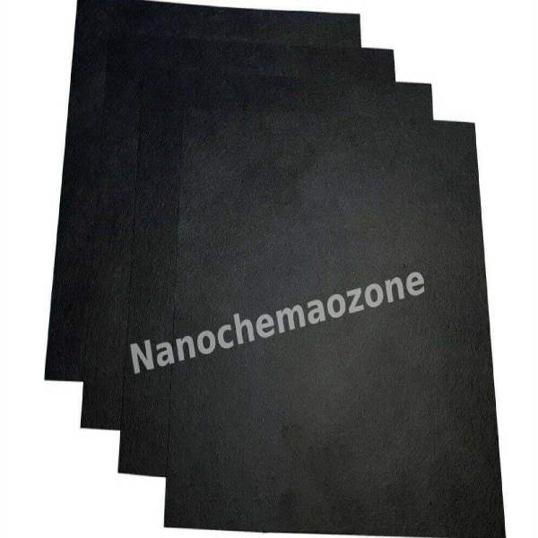
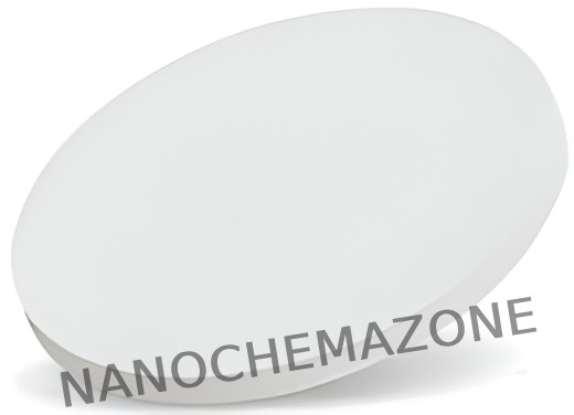
Silicon Nitride (Si3N4) Sputtering Targets, Purity: 99.5%, Size: 2”, Thickness: 0.250”, Dark Gray to Black

$465.00

Applications of Sputtering Targets;

Film deposition is accomplished using sputtering targets. A technique for sputtering thin films is called "deposition made by sputter targets," which entails eroding material from a "target" source onto a "substrate" like a silicon wafer. Etching of the target is done using semiconductor sputtering targets. When selectivity is not an issue and a high degree of etching anisotropy is required, sputter etching is the method of choice. By removing the target material through etching, sputter targets are also utilized for investigation. In secondary ion spectroscopy (SIMS), one example is when the target material is sputtered at a steady pace. Mass spectrometry is used to quantify the concentration and identity of spewed atoms as the target is sputtered.

The target material's composition may be ascertained and even very low concentrations of contaminants can be found with the aid of the sputtering target.

There is also an application area for sputtering targets in space. One type of space weathering that alters the chemical and physical characteristics of airless worlds like the Moon and asteroids is sputtering.

Zinc (Zn) Sputtering Targets, indium, Purity: 99.95%, Size: 2”, Thickness: 0.125”

$465.00

Product 

Zinc (Zn) Sputtering Targets, indium, Purity: 99.95%, Size: 2'', Thickness: 0.125''

CAS No.

7440‑66‑6

Appearance

Powder

Purity

≥99%,  ≥99.9%,  ≥95%

(Other purities are also available)

APS

Zn (black granules) (Size Can be customized), Ask for other available size ranges.

Ingredient

N/A

Molecular Weight

65.38 g/mol

Melting Point

419.5 °C

Boiling Point

 907 °C

Density

7.14 g/cm³

Product Codes

NCZ-1459K

Zinc Oxide (ZnO) Sputtering Targets, Purity: 99.999%, Size: 1”, Thickness: 0.250”

$466.00

Product 

Zinc Oxide (ZnO) Sputtering Targets, Purity: 99.999%, Size: 1'', Thickness: 0.250''

CAS No.

1314‑13‑2

Appearance

Powder

Purity

≥99%,  ≥99.9%,  ≥95%

(Other purities are also available)

APS

ZnO (black granules) (Size Can be customized), Ask for other available size ranges.

Ingredient

N/A

Molecular Weight

81.38 g/mol

Melting Point

~1975 °C

Boiling Point

~2360 °C

Density

 ~5.61 g/cm³

Product Codes

NCZ-1454K

Polyglutamic acid(PGA, Cosmetic grade) (439522)

Price range: $466.00 through $632.00
Select options This product has multiple variants. The options may be chosen on the product page
Polyglutamic acid(PGA, Cosmetic grade) (439522)
Synonym  Natto Gum, Sodium polyglutamate, γ-PGA Na, PGA, γ-PGA, γ-Polyglutamic acid Cas No  25513-46-6 Specifications
 
Appearance White to off white granular or powder, no agglomeration
Assay(HPLC) ≥92%
Loss on drying(105°C, 2h) ≤8%
Molecular wt(Da) 100,000-2,000,000
pH(10g/L, water solution, 25°C) 5.0-7.5
Transmittance(5g/L, water solution, 400nm) ≥95%
Heavy metals(Pb, mg/kg) ≤10
Total plate count(CFU/g) ≤100
  Product Codes- NCZ-2675K

Polyglutamic acid(PGA, Agriculture grade) (539522)

Price range: $466.00 through $632.00
Select options This product has multiple variants. The options may be chosen on the product page
Polyglutamic acid(PGA, Agriculture grade) (539522) Agricultural polyglutamic acid is a green environmentally-friendly fertilizer synergist that can increase fertilizer utilization from 30-35% to 40-50%, with an average utilization increase of 7-12% in nitrogen fertilizer, an average increase of 10-25% in crop yield and even 60% in some crops. Major strengths are listed as follows. 1. Rich nutrients that improve utilization; 2. Long-term slow release; 3. Improve soil physical and chemical properties; 4. Improve crop quality and yield; 5. Environmental friendly. Specifications
Appearance Yellow to off white powder with a few agglomeration
Assay(HPLC) ≥25%
Loss on drying(105°C, 2h) ≤6%
pH(10g/L, 25°C) 4.0-8.5
Heavy metals(Pb, mg/kg) ≤20
    Product Codes- NCZ-2676K

Lanthanum hexaboride(LaB6, 99.9%, -360 mesh) (575927)

$467.00
Select options This product has multiple variants. The options may be chosen on the product page
Lanthanum hexaboride(LaB6, 99.9%, -360 mesh) (575927)
 
Product Codes- NCZ-2698K

Lanthanum Calcium Manganate (La0.7Ca0.3MnO3) Sputtering Targets, Purity: 99.9%, Size: 4”, Thickness: 0.250”

$468.00
Select options This product has multiple variants. The options may be chosen on the product page

Applications of Sputtering Targets;

  • Sputtering targets is used for film deposition. The deposition made by sputter targets is a method of depositing thin films by sputtering that involves eroding material from a "target" source onto a "substrate" such as  a silicon wafer.
  • Semiconductor sputtering targets is used to etch the target. Sputter etching is chosen in cases where a high degree of etching anisotropy is needed and selectivity is not a concern.
  • Sputter targets is also used for analysis by etching away the target material.
One of the example occurs in secondary ion spectroscopy (SIMS), where the target sample is sputtered at a constant rate. As the target is sputtered, the concentration and identity of sputtered atoms are measured using mass spectrometry. By helping of the sputtering target, the composition of the target material can be determined and even extremely low concentrations of impurities are detected. Sputtering target has also application area in space. Sputtering is one of the forms of space weathering, a process that changes the physical and chemical properties of airless bodies, such as asteroids and the Moon.

Lanthanum Calcium Manganate (La0.7Ca0.3MnO3) Sputtering Targets, Purity: 99.9%, Size: 4”, Thickness: 0.250”

$468.00

Applications of Sputtering Targets;

Film deposition is accomplished using sputtering targets. A technique for sputtering thin films is called "deposition made by sputter targets," which entails eroding material from a "target" source onto a "substrate" like a silicon wafer. Etching of the target is done using semiconductor sputtering targets. When selectivity is not an issue and a high degree of etching anisotropy is required, sputter etching is the method of choice. By removing the target material through etching, sputter targets are also utilized for investigation. In secondary ion spectroscopy (SIMS), one example is when the target material is sputtered at a steady pace. Mass spectrometry is used to quantify the concentration and identity of spewed atoms as the target is sputtered.

The target material's composition may be ascertained and even very low concentrations of contaminants can be found with the aid of the sputtering target.

There is also an application area for sputtering targets in space. One type of space weathering that alters the chemical and physical characteristics of airless worlds like the Moon and asteroids is sputtering.

Lanthanum Titanate (LaTiO3) Sputtering Targets, Purity: 99.9%, Size: 1”, Thickness: 0.125”

$469.00

Applications of Sputtering Targets;

  • Sputtering targets is used for film deposition. The deposition made by sputter targets is a method of depositing thin films by sputtering that involves eroding material from a "target" source onto a "substrate" such as  a silicon wafer.
  • Semiconductor sputtering targets is used to etch the target. Sputter etching is chosen in cases where a high degree of etching anisotropy is needed and selectivity is not a concern.
  • Sputter targets is also used for analysis by etching away the target material.
One of the example occurs in secondary ion spectroscopy (SIMS), where the target sample is sputtered at a constant rate. As the target is sputtered, the concentration and identity of sputtered atoms are measured using mass spectrometry. By helping of the sputtering target, the composition of the target material can be determined and even extremely low concentrations of impurities are detected. Sputtering target has also application area in space. Sputtering is one of the forms of space weathering, a process that changes the physical and chemical properties of airless bodies, such as asteroids and the Moon.

Manganese (Mn) Sputtering Targets, indium, Purity: 99.95%, Size: 1”, Thickness: 0.125”

$469.00

Applications of Sputtering Targets;

For film deposition, sputtering targets are employed. A sputtering technique called "deposition made by sputter targets" entails eroding material from a "target" source onto a "substrate" like a silicon wafer. Targets are etched using semiconductor sputtering targets. When etching anisotropy is required to a great degree and selectivity is not an issue, sputter etching is the method of choice. By etching away the target material, sputter targets are also utilized for investigation. In one instance, the target sample is sputtered at a steady pace in secondary ion spectroscopy (SIMS). Using mass spectrometry, the concentration and identity of the spewed atoms are determined when the target is sputtered.

By helping of the sputtering target, the composition of the target material may be evaluated and even extremely tiny amounts of contaminants are recognized.

There is also an application area for sputtering targets in space. One type of space weathering that alters the chemical and physical characteristics of airless worlds like the Moon and asteroids is sputtering.

Molybdenum (Mo) Sputtering Targets, Purity: 99.95%, Size: 1”, Thickness: 0.250”

$469.00

Applications of Sputtering Targets;

Film deposition is accomplished using sputtering targets. A technique for sputtering thin films is called "deposition made by sputter targets," which entails eroding material from a "target" source onto a "substrate" like a silicon wafer. Etching of the target is done using semiconductor sputtering targets. When selectivity is not an issue and a high degree of etching anisotropy is required, sputter etching is the method of choice. By removing the target material through etching, sputter targets are also utilized for investigation. In secondary ion spectroscopy (SIMS), one example is when the target material is sputtered at a steady pace. Mass spectrometry is used to quantify the concentration and identity of spewed atoms as the target is sputtered.

By helping of the sputtering target, the composition of the target material may be evaluated and even extremely tiny amounts of contaminants are recognized.

There is also an application area for sputtering targets in space. One type of space weathering that alters the chemical and physical characteristics of airless worlds like the Moon and asteroids is sputtering.

Tungsten (W) Sputtering Targets, Purity: 99.95%, Size: 4”, Thickness: 0.125”

$469.00

Product 

Tungsten (W) Sputtering Targets, Purity: 99.95%, Size: 4'', Thickness: 0.125''

CAS No.

7440-33-7

Appearance

Powder

Purity

≥99%,  ≥99.9%,  ≥95%

(Other purities are also available)

APS

N/A  (Size Can be customized), Ask for other available size ranges.

Ingredient

N/A

Molecular Weight

 183.84 g/mol

Melting Point

3422 °C

Boiling Point

 5555 °C

Density

19.25 g/cm³

Product Codes

NCZ-1589K

Conductive Graphene Slurry in NMP, 1kg

$469.00
Product Conductive Graphene Slurry in NMP, 1kg
CAS No. 7782-42-5
Appearance Black viscous liquid
Purity ≥99%,  ≥99.9%,  ≥95%(Other purities are also available)
APS 1µm (Size Can be customized),  Ask for other available size range.
Ingredient C
Molecular Weight N/A
Melting Point N/A
Boiling Point N/A
Density 1.03 g/cm³
Product Codes NCZ-322I

Polyhydroxylated Fullerene (Fullerenols)/ C60, (-OH) Functionalized, Dispersed in Water, 4000 ppm Dry powder

Price range: $470.00 through $5,016.00
Select options This product has multiple variants. The options may be chosen on the product page
25 ml/420 € 100 ml/1390 € 500 ml/3240 € 1000 ml/4480 € Please contact us for quotes on larger quantities.

Polyhydroxylated Fullerene (Fullerenols)/ C60

(-OH) Functionalized, Dispersed in Water, 4000 ppm, Dry powder

The starting material is >98% purity C60 fullerenes. C60 bearing over 40 hydroxyl groups that have higher water solubility (>50 mg/mL). These exist as monodisperse nanoparticles in water, and have a valiant polishing effect. They exhibit superior antioxidant and anti-inflammatory properties.

Applications:

1. Pharmaceutical: Diagnostic reagents, super drugs, cosmetics, nuclear magnetic resonance (NMR) with the developer. DNA affinity, anti-HIV drugs, anti-cancer drugs, chemotherapy drugs, cosmetics additives and scientific research. 2. Energy: Solar battery, fuel cell, secondary battery. 3. Industry: Wear resistant material, flame retardant materials, lubricants, polymer additives, high-performance membrane, catalyst, artificial diamond, hard alloy, electric viscous fluid, ink filters, high-performance coatings, fire retardant coatings, manufacturing bioactive materials , memory materials, embedded molecular and other characteristics, composite materials etc. 4. Information industry: Semiconductor record medium, magnetic materials, printing ink, toner, ink, paper special purposes. 5. Electronic parts: Superconducting semiconductor, diodes, transistors, inductor. 6. Optical materials, electronic camera, fluorescence display tube, nonlinear optical materials. 7. Environment: Gas adsorption, gas storage.

Indium Oxide (In2O3) Sputtering Targets, Purity: 99.99%, Size: 2”, Thickness: 0.125”

$470.00

Applications of Sputtering Targets;

Film deposition is accomplished using sputtering targets. A technique for sputtering thin films is called "deposition made by sputter targets," which entails eroding material from a "target" source onto a "substrate" like a silicon wafer. Etching of the target is done using semiconductor sputtering targets. When selectivity is not an issue and a high degree of etching anisotropy is required, sputter etching is the method of choice. By removing the target material through etching, sputter targets are also utilized for investigation. In secondary ion spectroscopy (SIMS), one example is when the target material is sputtered at a steady pace. Mass spectrometry is used to quantify the concentration and identity of spewed atoms as the target is sputtered.

The target material's composition may be ascertained and even very low concentrations of contaminants can be found with the aid of the sputtering target.

There is also an application area for sputtering targets in space. One type of space weathering that alters the chemical and physical characteristics of airless worlds like the Moon and asteroids is sputtering.

Selenium (Se) Sputtering Targets, Purity: 99.999%, Size: 2”, Thickness: 0.250”

$470.00

Applications of Sputtering Targets;

Film deposition is accomplished using sputtering targets. A technique for sputtering thin films is called "deposition made by sputter targets," which entails eroding material from a "target" source onto a "substrate" like a silicon wafer. Etching of the target is done using semiconductor sputtering targets. When selectivity is not an issue and a high degree of etching anisotropy is required, sputter etching is the method of choice. By removing the target material through etching, sputter targets are also utilized for investigation. In secondary ion spectroscopy (SIMS), one example is when the target material is sputtered at a steady pace. Mass spectrometry is used to quantify the concentration and identity of spewed atoms as the target is sputtered.

The target material's composition may be ascertained and even very low concentrations of contaminants can be found with the aid of the sputtering target.

There is also an application area for sputtering targets in space. One type of space weathering that alters the chemical and physical characteristics of airless worlds like the Moon and asteroids is sputtering.

Tungsten (W) Sputtering Targets, elastomer, Purity: 99.95%, Size: 2”, Thickness: 0.125”

$470.00

Applications of Sputtering Targets;

Film deposition is accomplished using sputtering targets. A technique for sputtering thin films is called "deposition made by sputter targets," which entails eroding material from a "target" source onto a "substrate" like a silicon wafer. Etching of the target is done using semiconductor sputtering targets. When selectivity is not an issue and a high degree of etching anisotropy is required, sputter etching is the method of choice. By removing the target material through etching, sputter targets are also utilized for investigation. In secondary ion spectroscopy (SIMS), one example is when the target material is sputtered at a steady pace. Mass spectrometry is used to quantify the concentration and identity of spewed atoms as the target is sputtered. The target material's composition may be ascertained and even very low concentrations of contaminants can be found with the aid of the sputtering target. There is also an application area for sputtering targets in space. One type of space weathering that alters the chemical and physical characteristics of airless worlds like the Moon and asteroids is sputtering.

Vanadium Oxide (V2O5) Sputtering Targets, Purity: 99.9%, Size: 3”, Thickness: 0.125”

$470.00

Applications of Sputtering Targets;

Film deposition is accomplished using sputtering targets. A technique for sputtering thin films is called "deposition made by sputter targets," which entails eroding material from a "target" source onto a "substrate" like a silicon wafer. Etching of the target is done using semiconductor sputtering targets. When selectivity is not an issue and a high degree of etching anisotropy is required, sputter etching is the method of choice. By removing the target material through etching, sputter targets are also utilized for investigation. In secondary ion spectroscopy (SIMS), one example is when the target material is sputtered at a steady pace. Mass spectrometry is used to quantify the concentration and identity of spewed atoms as the target is sputtered.

The target material's composition may be ascertained and even very low concentrations of contaminants can be found with the aid of the sputtering target.

There is also an application area for sputtering targets in space. One type of space weathering that alters the chemical and physical characteristics of airless worlds like the Moon and asteroids is sputtering.

Zinc Oxide Nano-dispersion in Ethanol

$470.00
Select options This product has multiple variants. The options may be chosen on the product page
$470/500g

Product 

Zinc Oxide Nano-dispersion in Ethanol

CAS No.

1314-13-2

Appearance

Powder

Purity

≥99%,  ≥99.9%,  ≥95%

(Other purities are also available)

APS

~10–50 nm(Size Can be customized), Ask for other available size ranges.

Ingredient

N/A

Molecular Weight

81.38 g/mol

Melting Point

~1,975 °C

Boiling Point

~2,360 °C

Density

 ~5.61 g/cm³

Product Codes

NCZ-1223K

Tantalum Oxide (Ta2O5) Sputtering Targets, Purity: 99.99%, Size: 2”, Thickness: 0.250”

$470.00

Product 

Tantalum Oxide (Ta2O5) Sputtering Targets, Purity: 99.99%, Size: 2'', Thickness: 0.250''

CAS No.

1314-61-0

Appearance

Powder

Purity

≥99%,  ≥99.9%,  ≥95%

(Other purities are also available)

APS

N/A  (Size Can be customized), Ask for other available size ranges.

Ingredient

N/A

Molecular Weight

 441.89 g/mol

Melting Point

 ~1872 °C

Boiling Point

N/A

Density

~8.2 g/cm³

Product Codes

NCZ-1653K

Indium Zinc Oxide/IZO (InZnO) Sputtering Targets, Purity: 99.99%, Size: 2”, Thickness: 0.250”

$470.00

Product 

Indium Zinc Oxide/IZO (InZnO) Sputtering Targets, Purity: 99.99%, Size: 2'', Thickness: 0.250''

CAS No.

Indium oxide (In₂O₃): 1312-43-2
Zinc oxide (ZnO): 1314-13-2

Appearance

Powder

Purity

≥99%,  ≥99.9%,  ≥95%

(Other purities are also available)

APS

 N/A (Size Can be customized), Ask for other available size ranges.

Ingredient

N/A

Molecular Weight

Approx. 260–270 g/mol (depends on ratio)

Melting Point

Indium oxide: ~1910 °C Zinc oxide: ~1975 °C

Boiling Point

N/A

Density

~7.1 g/cm³

Product Codes

NCZ-2198K

Calcium sulfate whisker(CaSO4, L/D=10-80) (215675)

$470.00
Select options This product has multiple variants. The options may be chosen on the product page
Calcium sulfate whisker(CaSO4, L/D=10-80) (215675)

Chemical Composition: CaSO4

Appearance: White Powder

Particle Shape: Rod-like Shape Fiber

Purity(%): ≥95

Average Length(μm): 5-200

L/D Ratio: 10-80

Whiteness(%): >85

Gravity(g/cm3): 2.69

Loose Density(g/cm3): 0.1-0.6

Moisture(%): <1.5

Heat Resistance(°C): 1000

Melting Point(°C): 1450

Ph: 7+/-0.5

Mohs Hardness: 3

 
Product Codes- NCZ-2756K

Strontium Titanate (SrTiO3) Sputtering Target

Price range: $471.00 through $811.00
Select options This product has multiple variants. The options may be chosen on the product page

Product 

Strontium Titanate (SrTiO3) Sputtering Target

CAS No.

12060-59-2

Appearance

Powder

Purity

≥99%,  ≥99.9%,  ≥95%

(Other purities are also available)

APS

 NA (Size Can be customized), Ask for other available size ranges.

Ingredient

N/A

Molecular Weight

183.49 g/mol

Melting Point

~2,080 °C

Boiling Point

N\A

Density

~5.12 g/cm³

Product Codes

NCZ-1324K

Silicon Carbide (SiC) Sputtering Targets, Purity: 99.5%, Size: 1”, Thickness: 0.125”

$472.00

Product 

Silicon Carbide (SiC) Sputtering Targets, Purity: 99.5%, Size: 1'', Thickness: 0.125''

CAS No.

 409-21-2

Appearance

Powder

Purity

≥99%,  ≥99.9%,  ≥95%

(Other purities are also available)

APS

N/A  (Size Can be customized), Ask for other available size ranges.

Ingredient

N/A

Molecular Weight

 40.10 g/mol

Melting Point

~2,700 °C

Boiling Point

N/A

Density

~3.21 g/cm³

Product Codes

NCZ-1730K

Calcium Manganate (CaMnO3) Sputtering Targets, Purity: 99.9%, Size: 2”, Thickness: 0.125”

$473.00

Applications of Sputtering Targets;

Film deposition is accomplished using sputtering targets. A technique for sputtering thin films is called "deposition made by sputter targets," which entails eroding material from a "target" source onto a "substrate" like a silicon wafer. Etching of the target is done using semiconductor sputtering targets. When selectivity is not an issue and a high degree of etching anisotropy is required, sputter etching is the method of choice. By removing the target material through etching, sputter targets are also utilized for investigation. In secondary ion spectroscopy (SIMS), one example is when the target material is sputtered at a steady pace. Mass spectrometry is used to quantify the concentration and identity of spewed atoms as the target is sputtered.

The target material's composition may be ascertained and even very low concentrations of contaminants can be found with the aid of the sputtering target.

There is also an application area for sputtering targets in space. One type of space weathering that alters the chemical and physical characteristics of airless worlds like the Moon and asteroids is sputtering.

Silicon Carbide (SiC) Sputtering Targets, Purity: 99.5%, Size: 2”, Thickness: 0.125”

$473.00

Applications of Sputtering Targets;

Film deposition is accomplished using sputtering targets. A technique for sputtering thin films is called "deposition made by sputter targets," which entails eroding material from a "target" source onto a "substrate" like a silicon wafer. Etching of the target is done using semiconductor sputtering targets. When selectivity is not an issue and a high degree of etching anisotropy is required, sputter etching is the method of choice. By removing the target material through etching, sputter targets are also utilized for investigation. In secondary ion spectroscopy (SIMS), one example is when the target material is sputtered at a steady pace. Mass spectrometry is used to quantify the concentration and identity of spewed atoms as the target is sputtered.

The target material's composition may be ascertained and even very low concentrations of contaminants can be found with the aid of the sputtering target.

There is also an application area for sputtering targets in space. One type of space weathering that alters the chemical and physical characteristics of airless worlds like the Moon and asteroids is sputtering.

Molybdenum Titanium Aluminum Carbide (Mo2TiAlC2) MAX Phase Micron-Powder, 5g

$473.00
Select options This product has multiple variants. The options may be chosen on the product page
Product Molybdenum Titanium Aluminum Carbide (Mo2TiAlC2) MAX Phase Micron-Powder, 5g
CAS No. 7783-40-6
Appearance Gray to black fine
Purity ≥99%,  ≥99.9%,  ≥95%(Other purities are also available)
APS 1 – 5µm (Size Can be customized),  Ask for other available size range.
Ingredient Mo2Ti2AlC3
Molecular Weight 347.69 g/mol
Melting Point 1400 °C
Boiling Point N/A
Density 5.0–6.0 g/cm³
Product Codes NCZ-453I

Silicon Nitride (Si3N4) Sputtering Targets, Purity: 99.9%, Size: 2”, Thickness: 0.250”, White to Gray

$474.00

Applications of Sputtering Targets;

Film deposition is accomplished using sputtering targets. A technique for sputtering thin films is called "deposition made by sputter targets," which entails eroding material from a "target" source onto a "substrate" like a silicon wafer. Etching of the target is done using semiconductor sputtering targets. When selectivity is not an issue and a high degree of etching anisotropy is required, sputter etching is the method of choice. By removing the target material through etching, sputter targets are also utilized for investigation. In secondary ion spectroscopy (SIMS), one example is when the target material is sputtered at a steady pace. Mass spectrometry is used to quantify the concentration and identity of spewed atoms as the target is sputtered.

The target material's composition may be ascertained and even very low concentrations of contaminants can be found with the aid of the sputtering target.

There is also an application area for sputtering targets in space. One type of space weathering that alters the chemical and physical characteristics of airless worlds like the Moon and asteroids is sputtering.

Shape Memory Polymer NGM4520, Ether Type

Price range: $475.00 through $6,094.00
Select options This product has multiple variants. The options may be chosen on the product page

Applications:

Shape Memory Polymer (SMP) has myriad of advanced applications in different fields from daily life uses like textile to biomedicals. These applications include smart catheter, drug-delivery systems, biosensors, auto-repairing automobile parts, smart textile, self-healing materials, smart suture, artificial organs like muscles, and so on.

Gallium Antimonide (GaSb) Wafers, Size: 2”, Thickness: 500± 25 μm, Orientation: 111, Testing Grade

Price range: $475.00 through $2,196.00
Select options This product has multiple variants. The options may be chosen on the product page
Gallium Antimonide (GaSb) Wafers Size: 2”, Thickness: 500± 25 μm, Orientation: 111 Technical Properties: Quality  Testing Grade Size (inch)  2” Thickness

Gallium Antimonide (GaSb) Wafers, Size: 2”, Thickness: 500± 25 μm, Orientation: 100, Testing Grade

Price range: $475.00 through $2,196.00
Select options This product has multiple variants. The options may be chosen on the product page
Gallium Antimonide (GaSb) Wafers Size: 2”, Thickness: 500± 25 μm, Orientation: 100 Technical Properties: Quality  Testing Grade Size (inch)  2” Thickness

Lanthanum Calcium Manganate (La0.7Ca0.3MnO3) Sputtering Targets, Purity: 99.9%, Size: 1”, Thickness: 0.125”

$475.00
Select options This product has multiple variants. The options may be chosen on the product page

Applications of Sputtering Targets;

  • Sputtering targets is used for film deposition. The deposition made by sputter targets is a method of depositing thin films by sputtering that involves eroding material from a "target" source onto a "substrate" such as  a silicon wafer.
  • Semiconductor sputtering targets is used to etch the target. Sputter etching is chosen in cases where a high degree of etching anisotropy is needed and selectivity is not a concern.
  • Sputter targets is also used for analysis by etching away the target material.
One of the example occurs in secondary ion spectroscopy (SIMS), where the target sample is sputtered at a constant rate. As the target is sputtered, the concentration and identity of sputtered atoms are measured using mass spectrometry. By helping of the sputtering target, the composition of the target material can be determined and even extremely low concentrations of impurities are detected. Sputtering target has also application area in space. Sputtering is one of the forms of space weathering, a process that changes the physical and chemical properties of airless bodies, such as asteroids and the Moon.

Lanthanum Calcium Manganate (La0.7Ca0.3MnO3) Sputtering Targets, Purity: 99.9%, Size: 1”, Thickness: 0.125”

$475.00

Applications of Sputtering Targets;

Film deposition is accomplished using sputtering targets. A technique for sputtering thin films is called "deposition made by sputter targets," which entails eroding material from a "target" source onto a "substrate" like a silicon wafer. Etching of the target is done using semiconductor sputtering targets. When selectivity is not an issue and a high degree of etching anisotropy is required, sputter etching is the method of choice. By removing the target material through etching, sputter targets are also utilized for investigation. In secondary ion spectroscopy (SIMS), one example is when the target material is sputtered at a steady pace. Mass spectrometry is used to quantify the concentration and identity of spewed atoms as the target is sputtered.

The target material's composition may be ascertained and even very low concentrations of contaminants can be found with the aid of the sputtering target.

There is also an application area for sputtering targets in space. One type of space weathering that alters the chemical and physical characteristics of airless worlds like the Moon and asteroids is sputtering.

Manganese (Mn) Sputtering Targets, Purity: 99.95%, Size: 4”, Thickness: 0.250”

$475.00

Applications of Sputtering Targets;

Film deposition is accomplished using sputtering targets. A technique for sputtering thin films is called "deposition made by sputter targets," which entails eroding material from a "target" source onto a "substrate" like a silicon wafer. Etching of the target is done using semiconductor sputtering targets. When selectivity is not an issue and a high degree of etching anisotropy is required, sputter etching is the method of choice. By removing the target material through etching, sputter targets are also utilized for investigation. In secondary ion spectroscopy (SIMS), one example is when the target material is sputtered at a steady pace. Mass spectrometry is used to quantify the concentration and identity of spewed atoms as the target is sputtered.

The target material's composition may be ascertained and even very low concentrations of contaminants can be found with the aid of the sputtering target.

There is also an application area for sputtering targets in space. One type of space weathering that alters the chemical and physical characteristics of airless worlds like the Moon and asteroids is sputtering.

Manganese (Mn) Sputtering Targets, Purity: 99.95%, Size: 4”, Thickness: 0.125”

$475.00

Applications of Sputtering Targets;

Film deposition is accomplished using sputtering targets. A technique for sputtering thin films is called "deposition made by sputter targets," which entails eroding material from a "target" source onto a "substrate" like a silicon wafer. Etching of the target is done using semiconductor sputtering targets. When selectivity is not an issue and a high degree of etching anisotropy is required, sputter etching is the method of choice. By removing the target material through etching, sputter targets are also utilized for investigation. In secondary ion spectroscopy (SIMS), one example is when the target material is sputtered at a steady pace. Mass spectrometry is used to quantify the concentration and identity of spewed atoms as the target is sputtered.

By helping of the sputtering target, the composition of the target material may be evaluated and even extremely tiny amounts of contaminants are recognized.

There is also an application area for sputtering targets in space. One type of space weathering that alters the chemical and physical characteristics of airless worlds like the Moon and asteroids is sputtering.

Molybdenum Disilicide (MoSi2) Sputtering Targets, Purity: 99.95%, Size: 4”, Thickness: 0.125”

$475.00

Applications of Sputtering Targets;

Film deposition is accomplished using sputtering targets. A technique for sputtering thin films is called "deposition made by sputter targets," which entails eroding material from a "target" source onto a "substrate" like a silicon wafer. Etching of the target is done using semiconductor sputtering targets. When selectivity is not an issue and a high degree of etching anisotropy is required, sputter etching is the method of choice. By removing the target material through etching, sputter targets are also utilized for investigation. In secondary ion spectroscopy (SIMS), one example is when the target material is sputtered at a steady pace. Mass spectrometry is used to quantify the concentration and identity of spewed atoms as the target is sputtered.

By helping of the sputtering target, the composition of the target material may be evaluated and even extremely tiny amounts of contaminants are recognized.

There is also an application area for sputtering targets in space. One type of space weathering that alters the chemical and physical characteristics of airless worlds like the Moon and asteroids is sputtering.

Molybdenum Oxide (MoO3) Sputtering Targets, Purity: 99.9%, Size: 4”, Thickness: 0.125”

$475.00

Applications of Sputtering Targets;

Film deposition is accomplished using sputtering targets. A technique for sputtering thin films is called "deposition made by sputter targets," which entails eroding material from a "target" source onto a "substrate" like a silicon wafer. Etching of the target is done using semiconductor sputtering targets. When selectivity is not an issue and a high degree of etching anisotropy is required, sputter etching is the method of choice. By removing the target material through etching, sputter targets are also utilized for investigation. In secondary ion spectroscopy (SIMS), one example is when the target material is sputtered at a steady pace. Mass spectrometry is used to quantify the concentration and identity of spewed atoms as the target is sputtered.

By helping of the sputtering target, the composition of the target material may be evaluated and even extremely tiny amounts of contaminants are recognized.

There is also an application area for sputtering targets in space. One type of space weathering that alters the chemical and physical characteristics of airless worlds like the Moon and asteroids is sputtering.

Silicon (Si) Sputtering Targets, P-type, indium, Purity: 99.999%, Size: 2”, Thickness: 0.125”

$475.00

Applications of Sputtering Targets;

Film deposition is accomplished using sputtering targets. A technique for sputtering thin films is called "deposition made by sputter targets," which entails eroding material from a "target" source onto a "substrate" like a silicon wafer. Etching of the target is done using semiconductor sputtering targets. When selectivity is not an issue and a high degree of etching anisotropy is required, sputter etching is the method of choice. By removing the target material through etching, sputter targets are also utilized for investigation. In secondary ion spectroscopy (SIMS), one example is when the target material is sputtered at a steady pace. Mass spectrometry is used to quantify the concentration and identity of spewed atoms as the target is sputtered.

The target material's composition may be ascertained and even very low concentrations of contaminants can be found with the aid of the sputtering target.

There is also an application area for sputtering targets in space. One type of space weathering that alters the chemical and physical characteristics of airless worlds like the Moon and asteroids is sputtering.

Silicon (Si) Sputtering Targets, P-type, Purity: 99.999%, Size: 6”, Thickness: 0.125”

$475.00

Applications of Sputtering Targets;

Film deposition is accomplished using sputtering targets. A technique for sputtering thin films is called "deposition made by sputter targets," which entails eroding material from a "target" source onto a "substrate" like a silicon wafer. Etching of the target is done using semiconductor sputtering targets. When selectivity is not an issue and a high degree of etching anisotropy is required, sputter etching is the method of choice. By removing the target material through etching, sputter targets are also utilized for investigation. In secondary ion spectroscopy (SIMS), one example is when the target material is sputtered at a steady pace. Mass spectrometry is used to quantify the concentration and identity of spewed atoms as the target is sputtered.

The target material's composition may be ascertained and even very low concentrations of contaminants can be found with the aid of the sputtering target.

There is also an application area for sputtering targets in space. One type of space weathering that alters the chemical and physical characteristics of airless worlds like the Moon and asteroids is sputtering.

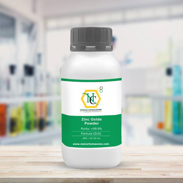
Zinc Oxide (ZnO) Sputtering Targets, Purity: 99.9%, Size: 2”, Thickness: 0.125”

$475.00

Applications of Sputtering Targets;

Film deposition is accomplished using sputtering targets. A technique for sputtering thin films is called "deposition made by sputter targets," which entails eroding material from a "target" source onto a "substrate" like a silicon wafer. Etching of the target is done using semiconductor sputtering targets. When selectivity is not an issue and a high degree of etching anisotropy is required, sputter etching is the method of choice. By removing the target material through etching, sputter targets are also utilized for investigation. In secondary ion spectroscopy (SIMS), one example is when the target material is sputtered at a steady pace. Mass spectrometry is used to quantify the concentration and identity of spewed atoms as the target is sputtered.

The target material's composition may be ascertained and even very low concentrations of contaminants can be found with the aid of the sputtering target.

There is also an application area for sputtering targets in space. One type of space weathering that alters the chemical and physical characteristics of airless worlds like the Moon and asteroids is sputtering.

Antimony Tin Oxide Nanoparticles/ Nanopowder Dispersion in aromatic 20%

$475.00
Select options This product has multiple variants. The options may be chosen on the product page
$475/500g

Product 

Antimony Tin Oxide Nanoparticles/ Nanopowder Dispersion in aromatic 20%

CAS No.

1332-09-8

Appearance

Powder

Purity

≥99%,  ≥99.9%,  ≥95%

(Other purities are also available)

APS

<20nm (Size Can be customized), Ask for other available size ranges.

Ingredient

N/A

Molecular Weight

~150–170 g/mol

Melting Point

~1,100 – 1,300 °C

Boiling Point

N/A

Density

~6.5–7.2 g/cm³

Product Codes

NCZ-1182K

Antimony Tin Oxide Nanoparticles/ Nanopowder Dispersion in Alcohols

$475.00
Select options This product has multiple variants. The options may be chosen on the product page
$475/500g

Product 

Antimony Tin Oxide Nanoparticles/ Nanopowder Dispersion in Alcohols

CAS No.

1332-09-8

Appearance

Powder

Purity

≥99%,  ≥99.9%,  ≥95%

(Other purities are also available)

APS

<20nm (Size Can be customized), Ask for other available size ranges.

Ingredient

N/A

Molecular Weight

~150–170 g/mol

Melting Point

~1,100 – 1,300 °C

Boiling Point

N/A

Density

~6.5–7.2 g/cm³

Product Codes

NCZ-1184K

Antimony Tin Oxide Nanoparticles/ Nanopowder Dispersion in water

$475.00
Select options This product has multiple variants. The options may be chosen on the product page
$475/500g

Product 

Antimony Tin Oxide Nanoparticles/ Nanopowder Dispersion in water

CAS No.

1332-09-8

Appearance

Powder

Purity

≥99%,  ≥99.9%,  ≥95%

(Other purities are also available)

APS

<20nm (Size Can be customized), Ask for other available size ranges.

Ingredient

N/A

Molecular Weight

Melting Point

~1,100 – 1,300 °C

Boiling Point

N/A

Density

~6.5–7.2 g/cm³

Product Codes

NCZ-1186K

Doped Tin Oxide Nanoparticles/ Nanopowder Dispersion in Aromatic(DTO)

$475.00
Select options This product has multiple variants. The options may be chosen on the product page
$475/500g

Product 

Doped Tin Oxide Nanoparticles/ Nanopowder Dispersion in Aromatic(DTO)

CAS No.

18282-10-5

Appearance

Powder

Purity

≥99%,  ≥99.9%,  ≥95%

(Other purities are also available)

APS

10~15nm (Size Can be customized), Ask for other available size ranges.

Ingredient

N/A

Molecular Weight

 ~160–165 g/mol

Melting Point

~1630 °C

Boiling Point

N/A

Density

 6.95 g/cm³

Product Codes

NCZ-1186K

Doped Tin Oxide Nanoparticles/ Nanopowder Dispersion in Alcohols(DTO)

$475.00
Select options This product has multiple variants. The options may be chosen on the product page
$475/500g

Product 

Doped Tin Oxide Nanoparticles/ Nanopowder Dispersion in Alcohols(DTO)

CAS No.

18282-10-5

Appearance

Powder

Purity

≥99%,  ≥99.9%,  ≥95%

(Other purities are also available)

APS

10~15nm (Size Can be customized), Ask for other available size ranges.

Ingredient

N/A

Molecular Weight

~150–165 g/mol

Melting Point

~1630 °C

Boiling Point

N/A

Density

 6.9–7.1 g/cm³

Product Codes

NCZ-1188K

Doped Tin Oxide Nanoparticles/ Nanopowder Dispersion in Water(DTO)

$475.00
Select options This product has multiple variants. The options may be chosen on the product page
$475/500g

Product 

Doped Tin Oxide Nanoparticles/ Nanopowder Dispersion in Water(DTO)

CAS No.

18282-10-5

Appearance

Powder

Purity

≥99%,  ≥99.9%,  ≥95%

(Other purities are also available)

APS

10~15nm (Size Can be customized), Ask for other available size ranges.

Ingredient

N/A

Molecular Weight

~150–165 g/mol

Melting Point

~1630 °C

Boiling Point

N/A

Density

 6.9–7.1 g/cm³

Product Codes

NCZ-1189K

Ytterbium Fluoride (YbF3, 99.9%,~5um)

$475.00
Select options This product has multiple variants. The options may be chosen on the product page
$475/500g

Product 

Ytterbium Fluoride (YbF3, 99.9%,~5um)

CAS No.

13760-80-0

Appearance

Powder

Purity

≥99%,  ≥99.9%,  ≥95%

(Other purities are also available)

APS

~5um (Size Can be customized), Ask for other available size ranges.

Ingredient

N/A

Molecular Weight

230.04 g/mol

Melting Point

~1,150 °C

Boiling Point

~2,200 °C

Density

~8.2 g/cm³

Product Codes

NCZ-1213K

Zinc Oxide Nano-dispersion in aromatic

$475.00
Select options This product has multiple variants. The options may be chosen on the product page
$475/500g

Product 

Zinc Oxide Nano-dispersion in aromatic

CAS No.

1314-13-2

Appearance

Powder

Purity

≥99%,  ≥99.9%,  ≥95%

(Other purities are also available)

APS

10–50 nm(Size Can be customized), Ask for other available size ranges.

Ingredient

N/A

Molecular Weight

81.38 g/mol

Melting Point

~1,975 °C

Boiling Point

~2,360 °C

Density

 ~5.61 g/cm³

Product Codes

NCZ-1219K

Zinc Oxide Nano-dispersion in water

Price range: $475.00 through $1,480.00
Select options This product has multiple variants. The options may be chosen on the product page
$475/500g
$1480/1000ML

Product 

Zinc Oxide Nano-dispersion in water

CAS No.

1314-13-2

Appearance

Powder

Purity

≥99%,  ≥99.9%,  ≥95%

(Other purities are also available)

APS

~10–50 nm(Size Can be customized), Ask for other available size ranges.

Ingredient

N/A

Molecular Weight

81.38 g/mol

Melting Point

~1,975 °C

Boiling Point

~2,360 °C

Density

 ~5.61 g/cm³

Product Codes

NCZ-1222K

Titanium Dioxide (TiO2) Sputtering Targets, Purity: 99.9%, Size: 3”, Thickness: 0.125”, Grey to Black

$476.00

Applications of Sputtering Targets;

Film deposition is accomplished using sputtering targets. A technique for sputtering thin films is called "deposition made by sputter targets," which entails eroding material from a "target" source onto a "substrate" like a silicon wafer. Etching of the target is done using semiconductor sputtering targets. When selectivity is not an issue and a high degree of etching anisotropy is required, sputter etching is the method of choice. By removing the target material through etching, sputter targets are also utilized for investigation. In secondary ion spectroscopy (SIMS), one example is when the target material is sputtered at a steady pace. Mass spectrometry is used to quantify the concentration and identity of spewed atoms as the target is sputtered.

The target material's composition may be ascertained and even very low concentrations of contaminants can be found with the aid of the sputtering target.

There is also an application area for sputtering targets in space. One type of space weathering that alters the chemical and physical characteristics of airless worlds like the Moon and asteroids is sputtering.

Tungsten Titanium (TiW) Sputtering Targets, Purity: 99.99%, Size: 6”, Thickness: 0.250”

$476.00

Product 

Tungsten Titanium (TiW) Sputtering Targets, Purity: 99.99%, Size: 6'', Thickness: 0.250''

CAS No.

58397-70-9

Appearance

Powder

Purity

≥99%,  ≥99.9%,  ≥95%

(Other purities are also available)

APS

N/A  (Size Can be customized), Ask for other available size ranges.

Ingredient

N/A

Molecular Weight

~231.71 g/mol

Melting Point

~2,700–3,200 °C

Boiling Point

~4,500–5,000 °C

Density

~14.5–17.0 g/cm³

Product Codes

NCZ-1553K

Titanium Boride (TiB2) Sputtering Targets, Purity: 99.5%, Size: 2”, Thickness: 0.125”

$476.00

Product 

Titanium Boride (TiB2) Sputtering Targets, Purity: 99.5%, Size: 2'', Thickness: 0.125''

CAS No.

 12045-63-5

Appearance

Powder

Purity

≥99%,  ≥99.9%,  ≥95%

(Other purities are also available)

APS

N/A  (Size Can be customized), Ask for other available size ranges.

Ingredient

N/A

Molecular Weight

69.49 g/mol

Melting Point

 ~3225 °C

Boiling Point

N/A

Density

 4.52 g/cm³

Product Codes

NCZ-1620K

Calcium Manganate (CaMnO3) Sputtering Targets, Purity: 99.9%, Size: 4”, Thickness: 0.250”

$476.00

Product 

Calcium Manganate (CaMnO3) Sputtering Targets, Purity: 99.9%, Size: 4'', Thickness: 0.250''

CAS No.

12058-85-6

Appearance

Powder

Purity

≥99%,  ≥99.9%,  ≥95%

(Other purities are also available)

APS

 N/A (Size Can be customized), Ask for other available size ranges.

Ingredient

N/A

Molecular Weight

157.87 g/mol

Melting Point

 Approx. 1400 °C (decomposes)

Boiling Point

N/A

Density

 ~4.7 g/cm³

Product Codes

NCZ-2356K

Barium (Ba) Sputtering Target

Price range: $478.00 through $1,182.00
Select options This product has multiple variants. The options may be chosen on the product page

Product 

Barium (Ba) Sputtering Target

CAS No.

7440-39-3

Appearance

Powder

Purity

≥99%,  ≥99.9%,  ≥95%

(Other purities are also available)

APS

 NA (Size Can be customized), Ask for other available size ranges.

Ingredient

N/A

Molecular Weight

137.33 g/mol

Melting Point

727 °C

Boiling Point

1,840 °C

Density

3.62 g/cm³

Product Codes

NCZ-1346K

Boron (B) Sputtering Target

Price range: $478.00 through $1,182.00
Select options This product has multiple variants. The options may be chosen on the product page

Product 

Boron (B) Sputtering Target

CAS No.

7440-42-8

Appearance

Powder

Purity

≥99%,  ≥99.9%,  ≥95%

(Other purities are also available)

APS

 NA (Size Can be customized), Ask for other available size ranges.

Ingredient

N/A

Molecular Weight

10.81 g/mol

Melting Point

~2,076 °C

Boiling Point

~4,000 °C

Density

~2.34 g/cm³

Product Codes

NCZ-1348K

Calcium (Ca) Sputtering Target

Price range: $478.00 through $1,182.00
Select options This product has multiple variants. The options may be chosen on the product page

Product 

Calcium (Ca) Sputtering Target

CAS No.

7440-70-2

Appearance

Powder

Purity

≥99%,  ≥99.9%,  ≥95%

(Other purities are also available)

APS

 NA (Size Can be customized), Ask for other available size ranges.

Ingredient

N/A

Molecular Weight

40.08 g/mol

Melting Point

 842 °C

Boiling Point

1,484 °C

Density

1.55 g/cm³

Product Codes

NCZ-1349K

Lithium Fluoride (LiF) Sputtering Target

Price range: $478.00 through $1,182.00
Select options This product has multiple variants. The options may be chosen on the product page

Product 

Lithium Fluoride (LiF) Sputtering Target

CAS No.

7789‑24‑4

Appearance

Powder

Purity

≥99%,  ≥99.9%,  ≥95%

(Other purities are also available)

APS

 NA (Size Can be customized), Ask for other available size ranges.

Ingredient

N/A

Molecular Weight

 25.94 g/mol

Melting Point

~845 °C

Boiling Point

~1,676 °C

Density

≈ 2.63–2.64 g/cm³

Product Codes

NCZ-1387K

Lithium Phosphate (Li3PO4) Sputtering Targets, Purity: 99.95%, Size: 2”, Thickness: 0.250”

$479.00

Applications of Sputtering Targets;

Film deposition is accomplished using sputtering targets. A technique for sputtering thin films is called "deposition made by sputter targets," which entails eroding material from a "target" source onto a "substrate" like a silicon wafer. Etching of the target is done using semiconductor sputtering targets. When selectivity is not an issue and a high degree of etching anisotropy is required, sputter etching is the method of choice. By removing the target material through etching, sputter targets are also utilized for investigation. In secondary ion spectroscopy (SIMS), one example is when the target material is sputtered at a steady pace. Mass spectrometry is used to quantify the concentration and identity of spewed atoms as the target is sputtered.

By helping of the sputtering target, the composition of the target material may be evaluated and even extremely tiny amounts of contaminants are recognized.

There is also an application area for sputtering targets in space. One type of space weathering that alters the chemical and physical characteristics of airless worlds like the Moon and asteroids is sputtering.

Cobalt Iron Boron (Co-Fe-B) Sputtering Targets, Purity: 99.9%, Size: 2”, Thickness: 0.125”

$480.00

Applications of Sputtering Targets;

Film deposition is accomplished using sputtering targets. A technique for sputtering thin films is called "deposition made by sputter targets," which entails eroding material from a "target" source onto a "substrate" like a silicon wafer.

Etching of the target is done using semiconductor sputtering targets. When selectivity is not an issue and a high degree of etching anisotropy is required, sputter etching is the method of choice. By removing the target material through etching, sputter targets are also utilized for investigation. In secondary ion spectroscopy (SIMS), one example is when the target material is sputtered at a steady pace. Mass spectrometry is used to quantify the concentration and identity of spewed atoms as the target is sputtered.

The target material's composition may be ascertained and even very low concentrations of contaminants can be found with the aid of the sputtering target.

There is also an application area for sputtering targets in space. One type of space weathering that alters the chemical and physical characteristics of airless worlds like the Moon and asteroids is sputtering.

An alloy consisting of cobalt, iron, and boron can be utilized as a sputtering target. Let's examine the possible uses for cobalt, iron, and boron alloys.

Tin (Sn) Sputtering Targets, Purity: 99.99%, Size: 4”, Thickness: 0.125”

$480.00

Applications of Sputtering Targets;

Film deposition is accomplished using sputtering targets. A technique for sputtering thin films is called "deposition made by sputter targets," which entails eroding material from a "target" source onto a "substrate" like a silicon wafer. Etching of the target is done using semiconductor sputtering targets. When selectivity is not an issue and a high degree of etching anisotropy is required, sputter etching is the method of choice. By removing the target material through etching, sputter targets are also utilized for investigation. In secondary ion spectroscopy (SIMS), one example is when the target material is sputtered at a steady pace. Mass spectrometry is used to quantify the concentration and identity of spewed atoms as the target is sputtered.

The target material's composition may be ascertained and even very low concentrations of contaminants can be found with the aid of the sputtering target.

There is also an application area for sputtering targets in space. One type of space weathering that alters the chemical and physical characteristics of airless worlds like the Moon and asteroids is sputtering.