Applications:
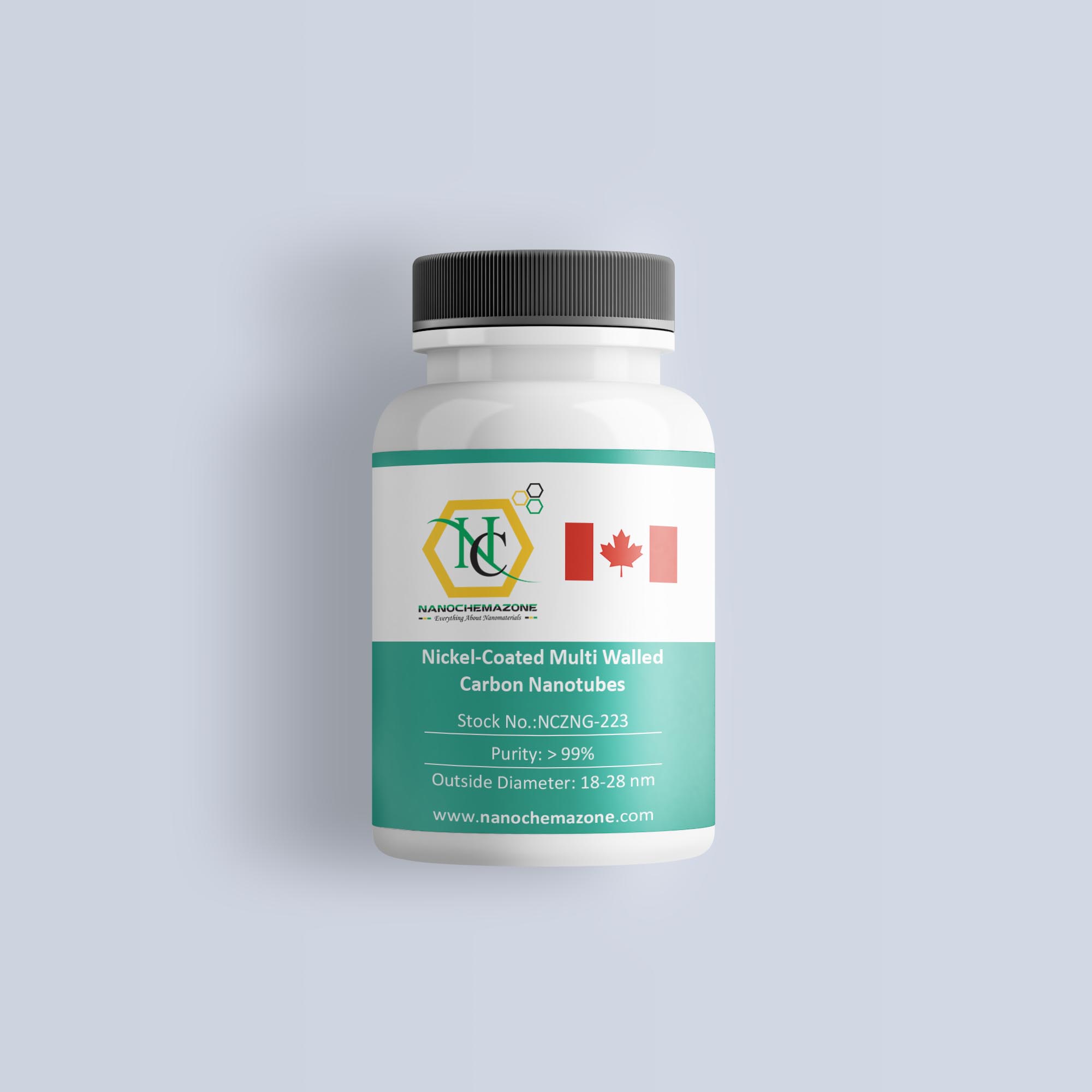
Nickel is coated on MWCNTs to have one dimentional magnetic material. Nickel is ferromagnetic material. MWCNTs are used as template for ferromagnetic nickel.
Nickel-coated MWCNTs show good magnetic properties. Nickel-coated MWCNTs have a variety of potential applications in different fields. These applications include
medicine, mechanics, electric-electronics, chemicals, energy and others. It can be applied in, 1-drug delivery, 2-biosensors, 3-CNT composites, 4-catalysis, 5-nanoprobes,
6-hydrogen storage, 7-lithium batteries, 8-gas-discharge tubes, 9-flat panel displays, 10-supercapacitors, 11-transistors, 12-solar cells, 13-photoluminescence, 14-templates