Boron Nitride (BN) Sputtering Targets, Purity: 99.5%, Size: 1”, Thickness: 0.250”

$408.00

Product 

Boron Nitride (BN) Sputtering Targets, Purity: 99.5%, Size: 1'', Thickness: 0.250''

CAS No.

 10043-11-5

Appearance

Powder

Purity

≥99%,  ≥99.9%,  ≥95%

(Other purities are also available)

APS

 N/A (Size Can be customized), Ask for other available size ranges.

Ingredient

N/A

Molecular Weight

24.82 g/mol

Melting Point

~2973 °C

Boiling Point

N/A

Density

~2.1 g/cm³

Product Codes

NCZ-2374K

Molybdenum Oxide (MoO3) Sputtering Targets, Purity: 99.9%, Size: 3”, Thickness: 0.125”

$409.00

Applications of Sputtering Targets;

Film deposition is accomplished using sputtering targets. A technique for sputtering thin films is called "deposition made by sputter targets," which entails eroding material from a "target" source onto a "substrate" like a silicon wafer. Etching of the target is done using semiconductor sputtering targets. When selectivity is not an issue and a high degree of etching anisotropy is required, sputter etching is the method of choice. By removing the target material through etching, sputter targets are also utilized for investigation. In secondary ion spectroscopy (SIMS), one example is when the target material is sputtered at a steady pace. Mass spectrometry is used to quantify the concentration and identity of spewed atoms as the target is sputtered.

Tantalum Oxide (Ta2O5) Sputtering Targets, Purity: 99.99%, Size: 2”, Thickness: 0.250”

$409.00

Applications of Sputtering Targets;

Film deposition is accomplished using sputtering targets. A technique for sputtering thin films is called "deposition made by sputter targets," which entails eroding material from a "target" source onto a "substrate" like a silicon wafer. Etching of the target is done using semiconductor sputtering targets. When selectivity is not an issue and a high degree of etching anisotropy is required, sputter etching is the method of choice. By removing the target material through etching, sputter targets are also utilized for investigation. In secondary ion spectroscopy (SIMS), one example is when the target material is sputtered at a steady pace. Mass spectrometry is used to quantify the concentration and identity of spewed atoms as the target is sputtered.

The target material's composition may be ascertained and even very low concentrations of contaminants can be found with the aid of the sputtering target.

There is also an application area for sputtering targets in space. One type of space weathering that alters the chemical and physical characteristics of airless worlds like the Moon and asteroids is sputtering.

Tungsten (W) Sputtering Targets, Purity: 99.95%, Size: 4”, Thickness: 0.125”

$409.00

Applications of Sputtering Targets;

Film deposition is accomplished using sputtering targets. A technique for sputtering thin films is called "deposition made by sputter targets," which entails eroding material from a "target" source onto a "substrate" like a silicon wafer. Etching of the target is done using semiconductor sputtering targets. When selectivity is not an issue and a high degree of etching anisotropy is required, sputter etching is the method of choice. By removing the target material through etching, sputter targets are also utilized for investigation. In secondary ion spectroscopy (SIMS), one example is when the target material is sputtered at a steady pace. Mass spectrometry is used to quantify the concentration and identity of spewed atoms as the target is sputtered.

The target material's composition may be ascertained and even very low concentrations of contaminants can be found with the aid of the sputtering target.

There is also an application area for sputtering targets in space. One type of space weathering that alters the chemical and physical characteristics of airless worlds like the Moon and asteroids is sputtering.

Lanthanum Strontium Manganate (La0.7Sr0.3MnO3) Sputtering Targets, Purity: 99.9%, Size: 1”, Thickness: 0.125”

$409.00

Product 

Lanthanum Strontium Manganate (La0.7Sr0.3MnO3) Sputtering Targets, Purity: 99.9%, Size: 1'', Thickness: 0.125''

CAS No.

 ~68189‑52‑4

Appearance

Powder

Purity

≥99%,  ≥99.9%,  ≥95%

(Other purities are also available)

APS

<5 µm (Size Can be customized), Ask for other available size ranges.

Ingredient

N/A

Molecular Weight

~234–237 g/mol

Melting Point

Decomposes before melting or boiling (≈ >1300 °C)

Boiling Point

N/A

Density

~6.3–6.5 g/cm³

Product Codes

NCZ-2109K

Aluminum Oxide (Al2O3) Sputtering Targets, Purity: 99.99%, Size: 2”, Thickness: 0.125”

$409.00

Product 

Aluminum Oxide (Al2O3) Sputtering Targets, Purity: 99.99%, Size: 2'', Thickness: 0.125''

CAS No.

 1344-28-1

Appearance

Powder

Purity

≥99%,  ≥99.9%,  ≥95%

(Other purities are also available)

APS

N/A (Size Can be customized), Ask for other available size ranges.

Ingredient

N/A

Molecular Weight

101.96 g/mol

Melting Point

~2,072 °C

Boiling Point

~2,977 °C

Density

~3.97–3.98 g/cm³

Product Codes

NCZ-2545K

Tungsten Titanium (TiW) Sputtering Targets, Purity: 99.99%, Size: 4”, Thickness: 0.250”

$410.00

Product 

Tungsten Titanium (TiW) Sputtering Targets, Purity: 99.99%, Size: 4'', Thickness: 0.250''

CAS No.

58397-70-9

Appearance

Powder

Purity

≥99%,  ≥99.9%,  ≥95%

(Other purities are also available)

APS

N/A  (Size Can be customized), Ask for other available size ranges.

Ingredient

N/A

Molecular Weight

~231.71 g/mol

Melting Point

~2,700–3,200 °C

Boiling Point

~4,500–5,000 °C

Density

~14.5–17.0 g/cm³

Product Codes

NCZ-1555K

Molybdenum Disilicide (MoSi2) Sputtering Targets, Purity: 99.95%, Size: 2”, Thickness: 0.125”

$411.00

Applications of Sputtering Targets;

Film deposition is accomplished using sputtering targets. A technique for sputtering thin films is called "deposition made by sputter targets," which entails eroding material from a "target" source onto a "substrate" like a silicon wafer. Etching of the target is done using semiconductor sputtering targets. When selectivity is not an issue and a high degree of etching anisotropy is required, sputter etching is the method of choice. By removing the target material through etching, sputter targets are also utilized for investigation. In secondary ion spectroscopy (SIMS), one example is when the target material is sputtered at a steady pace. Mass spectrometry is used to quantify the concentration and identity of spewed atoms as the target is sputtered.

By helping of the sputtering target, the composition of the target material may be evaluated and even extremely tiny amounts of contaminants are recognized.

There is also an application area for sputtering targets in space. One type of space weathering that alters the chemical and physical characteristics of airless worlds like the Moon and asteroids is sputtering.

Indium Zinc Oxide/IZO (InZnO) Sputtering Targets, Purity: 99.99%, Size: 2”, Thickness: 0.125”

$411.00

Product 

Indium Zinc Oxide/IZO (InZnO) Sputtering Targets, Purity: 99.99%, Size: 2'', Thickness: 0.125''

CAS No.

Indium oxide (In₂O₃): 1312-43-2
Zinc oxide (ZnO): 1314-13-2

Appearance

Powder

Purity

≥99%,  ≥99.9%,  ≥95%

(Other purities are also available)

APS

 N/A (Size Can be customized), Ask for other available size ranges.

Ingredient

N/A

Molecular Weight

Approx. 260–270 g/mol (depends on ratio)

Melting Point

Indium oxide: ~1910 °C Zinc oxide: ~1975 °C

Boiling Point

N/A

Density

~7.1 g/cm³

Product Codes

NCZ-2199K

Boron (B) Sputtering Targets, Purity: 99.9%, Size: 3”, Thickness: 0.125”

$413.00

Product 

Boron (B) Sputtering Targets, Purity: 99.9%, Size: 3'', Thickness: 0.125''

CAS No.

7440-42-8

Appearance

Powder

Purity

≥99%,  ≥99.9%,  ≥95%

(Other purities are also available)

APS

 N/A (Size Can be customized), Ask for other available size ranges.

Ingredient

N/A

Molecular Weight

 10.81 g/mol

Melting Point

~2076 °C

Boiling Point

 ~3927 °C

Density

 ~2.34 g/cm³

Product Codes

NCZ-2393K

Gold Nanostars, Size: 40-45 nm

Price range: $414.00 through $5,660.00
Select options This product has multiple variants. The options may be chosen on the product page
Gold Nanostars, 40-45 nm   Gold Nanostars are gold nanoparticles having multiple sharp and pointed branches in a genuine star-shaped. This unique shape enables them to have several thermoplasmonic and electromagnetic properties. Because gold nanoparticles have easy surface functionalization with biorecognition molecules, they are very suitable to use in biosensing studies and applications. Also, because gold nanoparticles are ultrafine in size, they are used diversely in the medical field in areas such as immunosensing, biolabels and drug delivery. These properties are valuable considering their use in disease diagnosis, treatment and prevention. Its application areas include usage in COVID-19 researches, biosensors, medical diagnostics, plasmon-enhanced or tip-enhanced spectroscopy, cancer therapies, and other biomedical and optical applications.

Indium Phosphide (InP) Wafers, Size: 2”, Thickness: 350± 25 μm, Orientation: 111, Single Side Polished, Testing Grade

Price range: $414.00 through $1,968.00
Select options This product has multiple variants. The options may be chosen on the product page
Indium Phosphide (InP) Wafers Size: 2”, Thickness: 350±25 μm, Orientation: 111 Technical Properties: Size (inch)  2” Thickness (μm)  350± 25 Dopant

Indium Phosphide (InP) Wafers, Size: 2”, Thickness: 350± 25 μm, Orientation: 100, Single Side Polished, Testing Grade

Price range: $414.00 through $1,968.00
Select options This product has multiple variants. The options may be chosen on the product page
Indium Phosphide (InP) Wafers Size: 2”, Thickness: 350±25 μm, Orientation: 100 Technical Properties: Size (inch)  2” Thickness (μm)  350± 25 Dopant

Silicon (Si) Sputtering Targets, N-type, Purity: 99.999%, Size: 6”, Thickness: 0.125”

$414.00

Applications of Sputtering Targets;

Film deposition is accomplished using sputtering targets. A technique for sputtering thin films is called "deposition made by sputter targets," which entails eroding material from a "target" source onto a "substrate" like a silicon wafer. Etching of the target is done using semiconductor sputtering targets. When selectivity is not an issue and a high degree of etching anisotropy is required, sputter etching is the method of choice. By removing the target material through etching, sputter targets are also utilized for investigation. In secondary ion spectroscopy (SIMS), one example is when the target material is sputtered at a steady pace. Mass spectrometry is used to quantify the concentration and identity of spewed atoms as the target is sputtered.

The target material's composition may be ascertained and even very low concentrations of contaminants can be found with the aid of the sputtering target.

There is also an application area for sputtering targets in space. One type of space weathering that alters the chemical and physical characteristics of airless worlds like the Moon and asteroids is sputtering.

Titanium Boride (TiB2) Sputtering Targets, Purity: 99.5%, Size: 2”, Thickness: 0.125”

$414.00

Applications of Sputtering Targets;

Film deposition is accomplished using sputtering targets. A technique for sputtering thin films is called "deposition made by sputter targets," which entails eroding material from a "target" source onto a "substrate" like a silicon wafer. Etching of the target is done using semiconductor sputtering targets. When selectivity is not an issue and a high degree of etching anisotropy is required, sputter etching is the method of choice. By removing the target material through etching, sputter targets are also utilized for investigation. In secondary ion spectroscopy (SIMS), one example is when the target material is sputtered at a steady pace. Mass spectrometry is used to quantify the concentration and identity of spewed atoms as the target is sputtered.

The target material's composition may be ascertained and even very low concentrations of contaminants can be found with the aid of the sputtering target.

There is also an application area for sputtering targets in space. One type of space weathering that alters the chemical and physical characteristics of airless worlds like the Moon and asteroids is sputtering.

Tungsten Titanium (TiW) Sputtering Targets, Purity: 99.99%, Size: 6”, Thickness: 0.250”

$414.00

Applications of Sputtering Targets;

Film deposition is accomplished using sputtering targets. A technique for sputtering thin films is called "deposition made by sputter targets," which entails eroding material from a "target" source onto a "substrate" like a silicon wafer. Etching of the target is done using semiconductor sputtering targets. When selectivity is not an issue and a high degree of etching anisotropy is required, sputter etching is the method of choice. By removing the target material through etching, sputter targets are also utilized for investigation. In secondary ion spectroscopy (SIMS), one example is when the target material is sputtered at a steady pace. Mass spectrometry is used to quantify the concentration and identity of spewed atoms as the target is sputtered.

The target material's composition may be ascertained and even very low concentrations of contaminants can be found with the aid of the sputtering target.

There is also an application area for sputtering targets in space. One type of space weathering that alters the chemical and physical characteristics of airless worlds like the Moon and asteroids is sputtering.

Silicon (Si) Sputtering Targets, P-type, Purity: 99.999%, Size: 4”, Thickness: 0.250”

$414.00

Product 

Silicon (Si) Sputtering Targets, P-type, Purity: 99.999%, Size: 4'', Thickness: 0.250''

CAS No.

7440-21-3

Appearance

Powder

Purity

≥99%,  ≥99.9%,  ≥95%

(Other purities are also available)

APS

N/A  (Size Can be customized), Ask for other available size ranges.

Ingredient

N/A

Molecular Weight

28.0855 g/mol

Melting Point

 1,414 °C

Boiling Point

3,265 °C

Density

 2.33 g/cm³

Product Codes

NCZ-1746K

Nickel Vanadium (NiV) Sputtering Targets, Purity: 99.95%, Size: 4”, Thickness: 0.125”

$414.00

Product 

Nickel Vanadium (NiV) Sputtering Targets, Purity: 99.95%, Size: 4'', Thickness: 0.125''

CAS No.

11137-91-4

Appearance

Powder

Purity

≥99%,  ≥99.9%,  ≥95%

(Other purities are also available)

APS

N/A (Size Can be customized), Ask for other available size ranges.

Ingredient

N/A

Molecular Weight

~57.9 g/mol

Melting Point

~1,350–1,450 °C

Boiling Point

N/A

Density

 ~8.5 g/cm³

Product Codes

NCZ-1824K

Gold (Au) Nanopowder/Nanoparticles, Purity: 99.99+%, Size: 28 nm

Price range: $415.00 through $1,822.00
Select options This product has multiple variants. The options may be chosen on the product page

Gold (Au) Nanopowder/Nanoparticles

Purity: 99.99+%, Size: 28 nm

Technical Properties:

Bulk Density (g/cm3) 0,92
True Density (g/cm3) 19,32
Color red - purple
Shape spherical
Crystal Structure cubic
Tmelting (oC) 1063
Tboiling (oC) 2966
Average Particle Size (nm) 28
Elemental Analysis Au Pb Cd Ag Fe Cu As, Sb
99.99 0.005 0.003 0.002 0.002 0.009 0.002

Applications:

Gold nanoparticle is used as chemical, medical and biological reagents. It is a well known and frequently used material in electronics and cosmetics industry.

Nickel Foil, Purity: 99.9+% , Thickness: 0.08mm, Width: 100mm

Price range: $415.00 through $1,860.00
Select options This product has multiple variants. The options may be chosen on the product page
1 piece / 415 € 5 pieces / 1860 € Please contact us for quotes on larger quantities ! Nickel Foil,

Calcium Manganate (CaMnO3) Sputtering Targets, Purity: 99.9%, Size: 4”, Thickness: 0.250”

$415.00

Applications of Sputtering Targets;

Film deposition is accomplished using sputtering targets. A technique for sputtering thin films is called "deposition made by sputter targets," which entails eroding material from a "target" source onto a "substrate" like a silicon wafer. Etching of the target is done using semiconductor sputtering targets. When selectivity is not an issue and a high degree of etching anisotropy is required, sputter etching is the method of choice. By removing the target material through etching, sputter targets are also utilized for investigation. In secondary ion spectroscopy (SIMS), one example is when the target material is sputtered at a steady pace. Mass spectrometry is used to quantify the concentration and identity of spewed atoms as the target is sputtered.

The target material's composition may be ascertained and even very low concentrations of contaminants can be found with the aid of the sputtering target.

There is also an application area for sputtering targets in space. One type of space weathering that alters the chemical and physical characteristics of airless worlds like the Moon and asteroids is sputtering.

4N (99.99%) Indium (In) Pellets Evaporation Materials

Price range: $415.00 through $2,163.00
Select options This product has multiple variants. The options may be chosen on the product page
Product 4N (99.99%) Indium (In) Pellets Evaporation Materials
CAS No. 7440-74-6
Appearance Silvery Lustrous Gray, Metallic 
Purity ≥99%,  ≥99.9%,  ≥95%(Other purities are also available)
APS 1-3mm (Size Can be customized),  Ask for other available size range.
Ingredient In
Molecular Weight 40.30 g/mol
Melting Point 157 °C
Boiling Point 2,072 °C
Density 7.3 g/cm³
Product Codes NCZ-129E
 

4N (99.99%) Indium (In) Pellets Evaporation Materials

Price range: $415.00 through $2,163.00
Select options This product has multiple variants. The options may be chosen on the product page
Product 4N (99.99%) Indium (In) Pellets Evaporation Materials
CAS No. 7440-74-6
Appearance Soft, ductile, silvery-white metal
Purity ≥99%,  ≥99.9%,  ≥95%(Other purities are also available)
APS 1–6mm (Size Can be customized),  Ask for other available size range.
Ingredient In
Molecular Weight 228.18 g/mol
Melting Point 156.6 °C
Boiling Point 2,072 °C
Density 7.13 g/cm³
Product Codes NCZ-169I
 

Neodymium Carbonate (Nd2(CO3)3) 99.5% 2N5

$415.00
Select options This product has multiple variants. The options may be chosen on the product page
Product Neodymium Carbonate (Nd2(CO3)3) 99.5% 2N5
CAS No. 13494-53-4
Appearance Pale green to white
Purity ≥99%,  ≥99.9%,  ≥95%(Other purities are also available)
APS 3–5µm (Size Can be customized),  Ask for other available size range.
Ingredient Nd2(CO3)3
Molecular Weight 336.23 g/mol
Melting Point N/A
Boiling Point N/A
Density 4.2 g/cm³
Product Codes NCZ-472I
 

Lanthanum Calcium Manganate (La0.7Ca0.3MnO3) Sputtering Targets, Purity: 99.9%, Size: 3”, Thickness: 0.125”

$415.00

Product 

Lanthanum Calcium Manganate (La0.7Ca0.3MnO3) Sputtering Targets, Purity: 99.9%, Size: 3'', Thickness: 0.125''

CAS No.

123273‑09‑6

Appearance

Powder

Purity

≥99%,  ≥99.9%,  ≥95%

(Other purities are also available)

APS

 N/A (Size Can be customized), Ask for other available size ranges.

Ingredient

N/A

Molecular Weight

 ~313.9 g/mol

Melting Point

 ~1,550 °C (approximate; ceramic decomposition likely above)

Boiling Point

N/A

Density

 ~5.3 g/cm³ @ room temp

Product Codes

NCZ-2154K

Carbon Nanotube Sponges, Size: 20 mm x 20 mm, Thickness: 3-4 mm

Price range: $416.00 through $1,771.00
Select options This product has multiple variants. The options may be chosen on the product page
Carbon Nanotube Sponges, Size: 20 mm x 20 mm, Thickness: 3-4 mm The carbon nanotube sponge structure is uniform and they possess good mechanical strength, good flexibility, high porosity and low density. They can be used as a purifying agent in order to absorb pollutants. These pollutants can be fertilizers, pesticides or pharmaceuticals found in water, energy storage materials, catalyst carriers or in high-efficiency composite materials.

Silicon (Si) Sputtering Targets, N-type, Purity: 99.999%, Size: 5”, Thickness: 0.250”

$417.00

Applications of Sputtering Targets;

Film deposition is accomplished using sputtering targets. A technique for sputtering thin films is called "deposition made by sputter targets," which entails eroding material from a "target" source onto a "substrate" like a silicon wafer. Etching of the target is done using semiconductor sputtering targets. When selectivity is not an issue and a high degree of etching anisotropy is required, sputter etching is the method of choice. By removing the target material through etching, sputter targets are also utilized for investigation. In secondary ion spectroscopy (SIMS), one example is when the target material is sputtered at a steady pace. Mass spectrometry is used to quantify the concentration and identity of spewed atoms as the target is sputtered.

The target material's composition may be ascertained and even very low concentrations of contaminants can be found with the aid of the sputtering target.

There is also an application area for sputtering targets in space. One type of space weathering that alters the chemical and physical characteristics of airless worlds like the Moon and asteroids is sputtering.

Silicon (Si) Sputtering Targets, undoped, Purity: 99.999%, Size: 4”, Thickness: 0.125”

$418.00

Product 

Silicon (Si) Sputtering Targets, undoped, Purity: 99.999%, Size: 4'', Thickness: 0.125''

CAS No.

7440-21-3

Appearance

Powder

Purity

≥99%,  ≥99.9%,  ≥95%

(Other purities are also available)

APS

N/A  (Size Can be customized), Ask for other available size ranges.

Ingredient

N/A

Molecular Weight

28.0855 g/mol

Melting Point

1,414 °C

Boiling Point

 3,265 °C

Density

 2.33 g/cm³

Product Codes

NCZ-1731K

Silicon Carbide Wafer (SiC-4H) – 4H, Size: 2”, Thickness: 350 μm, Testing Grade, 4H Area: 80%

Price range: $419.00 through $1,847.00
Select options This product has multiple variants. The options may be chosen on the product page
1 piece/380 € 5 pieces/1675 €                           Please contact us for quotes on larger quantities !!!

Silicon Carbide Wafer (SiC-4H) - 4H

Size: 2'' , Thickness: 350 μm, 4H Area: 80%

Technical Properties:

Quality  Testing Grade
Size (inch)  2”
Thickness (μm)  350
Ra  ≤1
4H area  80%
Orientation  4°±0.5°
Resistivity   0.015-0.03
TTV  ≤25
Bow  ≤30
Warp  ≤35
OF Length  16±2
IF Length  8±1

Fields of Application for Silicon Carbide (SiC-4H)- 4H Wafer

Silicon carbide (SiC) is a rare compound of silicon and carbon which is synthetically produced. Silicon carbide (SiC) wafer has great electrical properties and excellent thermal properties. Silicon carbide (SiC) wafer has low thermal expansion. Silicon carbide (SiC) wafer has superior hardness properties. Silicon carbide (SiC) wafer performs well at high temperatures. Also, silicon carbide (SiC) wafer has high resistance to corrosion, erosion and oxidation. In addition to, silicon carbide (SiC) wafer is also more shiny than either diamonds or cubic zirconia. Silicon carbide (SiC) crystals have unique physical and electronic properties. Silicon Carbide based devices have been used for short wavelength opto-electronic, high temperature, radiation resistant applications.  The high-power and high-frequency electronic devices made with SiC are superior to Si and GaAs based devices.  Below are some popular applications of SiC substrates. SiC based devices have low lattice mismatch with III-nitride epitaxial layers.  They have high thermal conductivity and can be used for the monitoring of combustion processes and for all sorts of UV-detection.  SiC-based semiconductor devices can work under very hostile environments, such as high temperature, high power, and high radiation conditions. SiC is used for the fabrication of very high-voltage and high-power devices such as diodes, power transistors, and high power microwave devices. Compared to conventional Si-devices, SiC-based power devices have faster switching speed higher voltages, lower parasitic resistances, smaller size, less cooling required due to high-temperature capability. While Silicon carbide (SiC-4H) - 4H wafer has superior electronic properties, silicon carbide (SiC-6H) – 6H wafer is most easily prepared and best studied.
  • Silicon carbide (SiC) wafer is used for hybrid and electric vehicles.
  • Silicon carbide (SiC) wafer is used for green energy generation.
  • Silicon carbide (SiC) wafer is used for LEDs.
  • Silicon carbide (SiC) wafer is used for many other emerging markets.

Silicon Carbide Wafer (SiC-4H)- 4H, Size: 2”, Thickness: 350 μm, Mechanical Grade, 4H Area: 95%

Price range: $419.00 through $1,847.00
Select options This product has multiple variants. The options may be chosen on the product page
1 piece/380  5 pieces/1675                            Please contact us for quotes on larger quantities !!!

Silicon Carbide Wafer (SiC-4H) - 4H

Size: 2'', Thickness: 350 μm, 4H Area: 95%

Technical Properties:

Quality Dummy Grade
Size (inch)  2”
Thickness (μm)  350
Ra  ≤1
4H area  95%
Orientation  4°±0.5°
Resistivity   0.015-0.03
TTV  ≤15
Bow  ≤25
Warp  ≤35
OF Length  16±2
IF Length  8±1

Fields of Application for Silicon Carbide (SiC-4H)- 4H Wafer

Silicon carbide (SiC) is a rare compound of silicon and carbon which is synthetically produced. Silicon carbide (SiC) wafer has great electrical properties and excellent thermal properties. Silicon carbide (SiC) wafer has low thermal expansion. Silicon carbide (SiC) wafer has superior hardness properties. Silicon carbide (SiC) wafer performs well at high temperatures. Also, silicon carbide (SiC) wafer has high resistance to corrosion, erosion and oxidation. In addition to, silicon carbide (SiC) wafer is also more shiny than either diamonds or cubic zirconia. Silicon carbide (SiC) crystals have unique physical and electronic properties. Silicon Carbide based devices have been used for short wavelength opto-electronic, high temperature, radiation resistant applications.  The high-power and high-frequency electronic devices made with SiC are superior to Si and GaAs based devices.  Below are some popular applications of SiC substrates. SiC based devices have low lattice mismatch with III-nitride epitaxial layers.  They have high thermal conductivity and can be used for the monitoring of combustion processes and for all sorts of UV-detection.  SiC-based semiconductor devices can work under very hostile environments, such as high temperature, high power, and high radiation conditions. SiC is used for the fabrication of very high-voltage and high-power devices such as diodes, power transistors, and high power microwave devices. Compared to conventional Si-devices, SiC-based power devices have faster switching speed higher voltages, lower parasitic resistances, smaller size, less cooling required due to high-temperature capability. While Silicon carbide (SiC-4H) - 4H wafer has superior electronic properties, silicon carbide (SiC-6H) – 6H wafer is most easily prepared and best studied.
  • Silicon carbide (SiC) wafer is used for hybrid and electric vehicles.
  • Silicon carbide (SiC) wafer is used for green energy generation.
  • Silicon carbide (SiC) wafer is used for LEDs.
  • Silicon carbide (SiC) wafer is used for many other emerging markets.

Carboxyl Graphene Quantum Dots Solution, 1mg/mL

Price range: $419.00 through $789.00
Select options This product has multiple variants. The options may be chosen on the product page
Product Carboxyl Graphene Quantum Dots Solution, 1mg/mL
CAS No. 7782-42-5
Appearance Black or dark brown
Purity ≥99%,  ≥99.9%,  ≥95%(Other purities are also available)
APS 1–5µm (Size Can be customized),  Ask for other available size range.
Ingredient CₓOᵧH_z
Molecular Weight 12.01 g/mol
Melting Point N/A
Boiling Point N/A
Density 0.45 g/cm³
Product Codes NCZ-305I

Chromium Oxide (Cr2O3) Sputtering Targets, Purity: 99.8%-99.9%, Size: 2”, Thickness: 0.250”

$420.00

Applications of Sputtering Targets;

Film deposition is accomplished using sputtering targets. A technique for sputtering thin films is called "deposition made by sputter targets," which entails eroding material from a "target" source onto a "substrate" like a silicon wafer. Etching of the target is done using semiconductor sputtering targets. When selectivity is not an issue and a high degree of etching anisotropy is required, sputter etching is the method of choice. By removing the target material through etching, sputter targets are also utilized for investigation. In secondary ion spectroscopy (SIMS), one example is when the target material is sputtered at a steady pace. Mass spectrometry is used to quantify the concentration and identity of spewed atoms as the target is sputtered.

The target material's composition may be ascertained and even very low concentrations of contaminants can be found with the aid of the sputtering target.

There is also an application area for sputtering targets in space. One type of space weathering that alters the chemical and physical characteristics of airless worlds like the Moon and asteroids is sputtering.

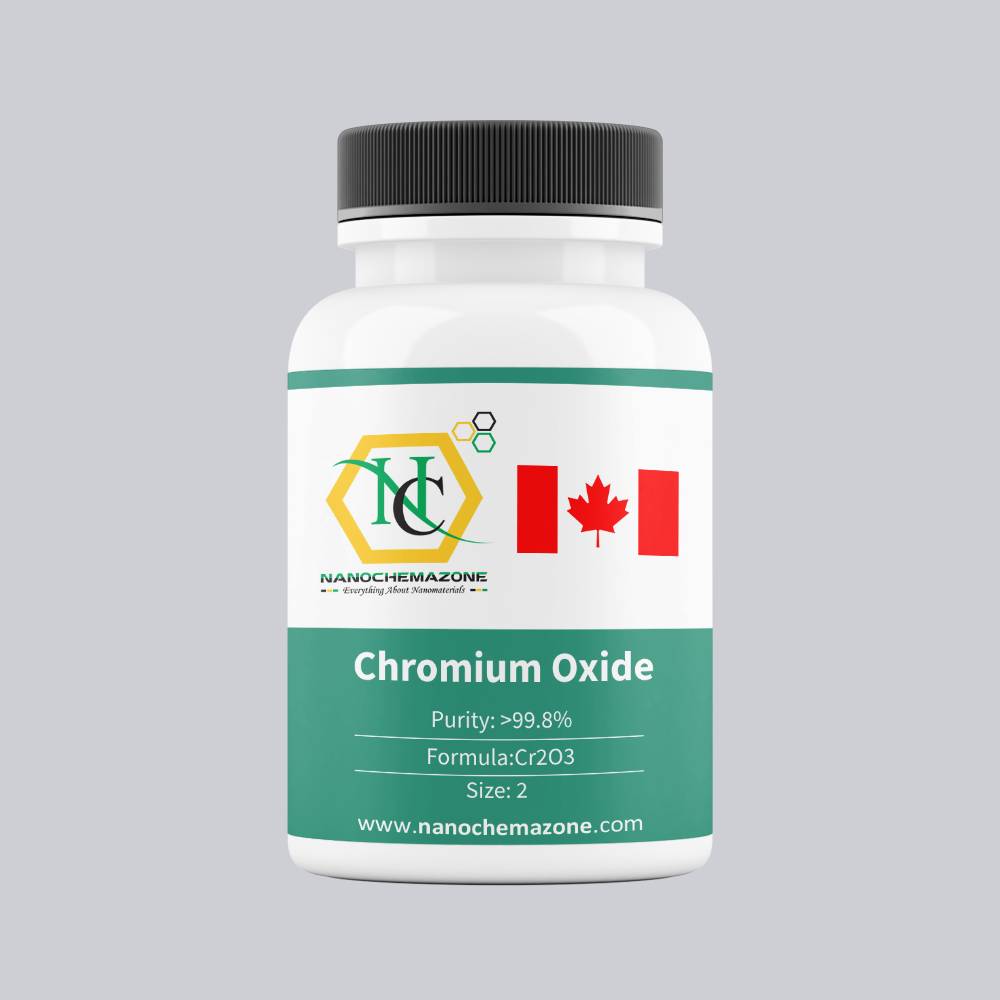
The inorganic chemical with the formula Cr2O3 is chromium oxide. Applications for chromium oxide sputtering targets are numerous. Let's examine a few instances where chromium oxide sputtering targets are employed instead. Low friction coefficients and high hardness values are displayed by Cr2O3 thin films. Because of these qualities, chromium oxide is a strong contender to take the place of Al2O3 or transition metal nitrides in certain applications.

Cobalt (Co) Sputtering Targets, Purity: 99.95%, Size: 6”, Thickness: 0.125”

$420.00

Applications of Sputtering Targets;

Film deposition is accomplished using sputtering targets. A technique for sputtering thin films is called "deposition made by sputter targets," which entails eroding material from a "target" source onto a "substrate" like a silicon wafer. Etching of the target is done using semiconductor sputtering targets. When selectivity is not an issue and a high degree of etching anisotropy is required, sputter etching is the method of choice. By removing the target material through etching, sputter targets are also utilized for investigation. In secondary ion spectroscopy (SIMS), one example is when the target material is sputtered at a steady pace. Mass spectrometry is used to quantify the concentration and identity of spewed atoms as the target is sputtered.

The target material's composition may be ascertained and even very low concentrations of contaminants can be found with the aid of the sputtering target.

There is also an application area for sputtering targets in space. One type of space weathering that alters the chemical and physical characteristics of airless worlds like the Moon and asteroids is sputtering.

The chemical element cobalt has the atomic number 27 and the symbol Co. Cobalt is a silver-gray, hard, and shiny metal. Because it is one of only three room temperature ferromagnets with unaxial symmetry and hence suitability for digital recording, cobalt is employed in the production of high-strength, wear-resistant alloys as well as magnetic recording.

Cobalt Iron Boron (Co-Fe-B) Sputtering Targets, Purity: 99.9%, Size: 1”, Thickness: 0.125”

$420.00

Applications of Sputtering Targets;

Film deposition is accomplished using sputtering targets. A technique for sputtering thin films is called "deposition made by sputter targets," which entails eroding material from a "target" source onto a "substrate" like a silicon wafer. Etching of the target is done using semiconductor sputtering targets. When selectivity is not an issue and a high degree of etching anisotropy is required, sputter etching is the method of choice. By removing the target material through etching, sputter targets are also utilized for investigation. In secondary ion spectroscopy (SIMS), one example is when the target material is sputtered at a steady pace. Mass spectrometry is used to quantify the concentration and identity of spewed atoms as the target is sputtered.

The target material's composition may be ascertained and even very low concentrations of contaminants can be found with the aid of the sputtering target.

There is also an application area for sputtering targets in space. One type of space weathering that alters the chemical and physical characteristics of airless worlds like the Moon and asteroids is sputtering.

An alloy consisting of cobalt, iron, and boron can be utilized as a sputtering target. Let's examine the possible uses for cobalt, iron, and boron alloys.

Several desirable characteristics of boron alloys including transition metals, such as cobalt iron boron, include high melting points and hardness, strong resistance to wear and corrosion, superior electrical conductivity.

Nickel (Ni) Sputtering Targets, Purity: 99.9%, Size: 8”, Thickness: 0.250”

$420.00

Applications of Sputtering Targets;

Film deposition is accomplished using sputtering targets. A technique for sputtering thin films is called "deposition made by sputter targets," which entails eroding material from a "target" source onto a "substrate" like a silicon wafer. Etching of the target is done using semiconductor sputtering targets. When selectivity is not an issue and a high degree of etching anisotropy is required, sputter etching is the method of choice. By removing the target material through etching, sputter targets are also utilized for investigation. In secondary ion spectroscopy (SIMS), one example is when the target material is sputtered at a steady pace. Mass spectrometry is used to quantify the concentration and identity of spewed atoms as the target is sputtered.

The target material's composition may be ascertained and even very low concentrations of contaminants can be found with the aid of the sputtering target.

There is also an application area for sputtering targets in space. One type of space weathering that alters the chemical and physical characteristics of airless worlds like the Moon and asteroids is sputtering.

Silicon Nitride (Si3N4) Sputtering Targets, Purity: 99.9%, Size: 2”, Thickness: 0.125”, White to Gray

$420.00

Applications of Sputtering Targets;

Film deposition is accomplished using sputtering targets. A technique for sputtering thin films is called "deposition made by sputter targets," which entails eroding material from a "target" source onto a "substrate" like a silicon wafer. Etching of the target is done using semiconductor sputtering targets. When selectivity is not an issue and a high degree of etching anisotropy is required, sputter etching is the method of choice. By removing the target material through etching, sputter targets are also utilized for investigation. In secondary ion spectroscopy (SIMS), one example is when the target material is sputtered at a steady pace. Mass spectrometry is used to quantify the concentration and identity of spewed atoms as the target is sputtered.

The target material's composition may be ascertained and even very low concentrations of contaminants can be found with the aid of the sputtering target.

There is also an application area for sputtering targets in space. One type of space weathering that alters the chemical and physical characteristics of airless worlds like the Moon and asteroids is sputtering.

Silicon Carbide (SiC) Sputtering Targets, Purity: 99.5%, Size: 1”, Thickness: 0.250”

$420.00

Applications of Sputtering Targets;

Film deposition is accomplished using sputtering targets. A technique for sputtering thin films is called "deposition made by sputter targets," which entails eroding material from a "target" source onto a "substrate" like a silicon wafer. Etching of the target is done using semiconductor sputtering targets. When selectivity is not an issue and a high degree of etching anisotropy is required, sputter etching is the method of choice. By removing the target material through etching, sputter targets are also utilized for investigation. In secondary ion spectroscopy (SIMS), one example is when the target material is sputtered at a steady pace. Mass spectrometry is used to quantify the concentration and identity of spewed atoms as the target is sputtered.

The target material's composition may be ascertained and even very low concentrations of contaminants can be found with the aid of the sputtering target.

There is also an application area for sputtering targets in space. One type of space weathering that alters the chemical and physical characteristics of airless worlds like the Moon and asteroids is sputtering.

Silicon (Si) Sputtering Targets, P-type, Purity: 99.999%, Size: 6”, Thickness: 0.250”

$420.00

Applications of Sputtering Targets;

Film deposition is accomplished using sputtering targets. A technique for sputtering thin films is called "deposition made by sputter targets," which entails eroding material from a "target" source onto a "substrate" like a silicon wafer. Etching of the target is done using semiconductor sputtering targets. When selectivity is not an issue and a high degree of etching anisotropy is required, sputter etching is the method of choice. By removing the target material through etching, sputter targets are also utilized for investigation. In secondary ion spectroscopy (SIMS), one example is when the target material is sputtered at a steady pace. Mass spectrometry is used to quantify the concentration and identity of spewed atoms as the target is sputtered.

Even very low quantities of contaminants can be detected with the aid of the sputtering target, allowing for the determination of the target material's composition.

Applications for sputtering targets are also found in space. One type of space weathering is sputtering, which modifies the chemical and physical characteristics of airless worlds like the Moon and asteroids.

Yttrium Oxide (Y2O3) Sputtering Target

Price range: $420.00 through $948.00
Select options This product has multiple variants. The options may be chosen on the product page

Product 

Yttrium Oxide (Y2O3) Sputtering Target

CAS No.

 1314-36-9

Appearance

Powder

Purity

≥99%,  ≥99.9%,  ≥95%

(Other purities are also available)

APS

 NA (Size Can be customized), Ask for other available size ranges.

Ingredient

N/A

Molecular Weight

225.81 g/mol

Melting Point

~2,430 °C

Boiling Point

~4,300 °C

Density

~5.01 g/cm³

Product Codes

NCZ-1330K

Magnesium Fluoride (MgF2) Sputtering Target

Price range: $421.00 through $975.00
Select options This product has multiple variants. The options may be chosen on the product page

Product 

Magnesium Fluoride (MgF2) Sputtering Target

CAS No.

7783-40-6

Appearance

Powder

Purity

≥99%,  ≥99.9%,  ≥95%

(Other purities are also available)

APS

 NA (Size Can be customized), Ask for other available size ranges.

Ingredient

N/A

Molecular Weight

62.30 g/mol

Melting Point

~1,261 °C

Boiling Point

~2,260 °C

Density

 ~3.15 g/cm³

Product Codes

NCZ-1340K

Permalloy (Ni-Fe-Mo) Sputtering Targets, Size: 4”, Thickness: 0.250”

$422.00

Applications of Sputtering Targets;

Film deposition is accomplished using sputtering targets. A technique for sputtering thin films is called "deposition made by sputter targets," which entails eroding material from a "target" source onto a "substrate" like a silicon wafer. Etching of the target is done using semiconductor sputtering targets. When selectivity is not an issue and a high degree of etching anisotropy is required, sputter etching is the method of choice. By removing the target material through etching, sputter targets are also utilized for investigation. In secondary ion spectroscopy (SIMS), one example is when the target material is sputtered at a steady pace. Mass spectrometry is used to quantify the concentration and identity of spewed atoms as the target is sputtered.

The target material's composition may be ascertained and even very low concentrations of contaminants can be found with the aid of the sputtering target.

There is also an application area for sputtering targets in space. One type of space weathering that alters the chemical and physical characteristics of airless worlds like the Moon and asteroids is sputtering.

Tungsten Disulfide (WS2) Sputtering Targets, Purity: 99.9%, Size: 5”, Thickness: 0.125”

$422.00

Applications of Sputtering Targets;

Film deposition is accomplished using sputtering targets. A technique for sputtering thin films is called "deposition made by sputter targets," which entails eroding material from a "target" source onto a "substrate" like a silicon wafer. Etching of the target is done using semiconductor sputtering targets. When selectivity is not an issue and a high degree of etching anisotropy is required, sputter etching is the method of choice. By removing the target material through etching, sputter targets are also utilized for investigation. In secondary ion spectroscopy (SIMS), one example is when the target material is sputtered at a steady pace. Mass spectrometry is used to quantify the concentration and identity of spewed atoms as the target is sputtered.

The target material's composition may be ascertained and even very low concentrations of contaminants can be found with the aid of the sputtering target.

There is also an application area for sputtering targets in space. One type of space weathering that alters the chemical and physical characteristics of airless worlds like the Moon and asteroids is sputtering.

Monolayer Graphene on SiO2/Si Substrate, Size: 4″

Price range: $423.00 through $1,864.00
Select options This product has multiple variants. The options may be chosen on the product page

Applications

Graphene research; Supercapacitors; Catalyst; Solar energy; Graphene optoelectronics, plasmonics and nanophotonics; Graphene semiconductor chips; Conductive graphene film; Graphene computer memory; Biomaterials and Bioelectronics.

Hydrothermal Synthesis Autoclave Reactor with PTFE Lined Vessel 500 ml

Price range: $423.00 through $1,845.00
Select options This product has multiple variants. The options may be chosen on the product page
APPLICATIONs
  • Chemical synthesis
  • Synthesizing of nanoparticles
  • For cultured crystal growth
  • Polymerization reaction
  • Hydrothermal decomposition
  • Catalyst synthesis
  • Hydrothermal oxidation
  • Hydrothermal precipitation
  • Material Digester / digestion
  • Crystallization process
  • Dissolve of heavy metals, refractory material, organic chemicals etc.

Antimony (Sb) Sputtering Target

Price range: $423.00 through $930.00
Select options This product has multiple variants. The options may be chosen on the product page

Product 

Antimony (Sb) Sputtering Target

CAS No.

7440-36-0

Appearance

Powder

Purity

≥99%,  ≥99.9%,  ≥95%

(Other purities are also available)

APS

 NA (Size Can be customized), Ask for other available size ranges.

Ingredient

N/A

Molecular Weight

121.76 g/mol

Melting Point

630.63 °C

Boiling Point

1,580 °C

Density

~6.697 g/cm³

Product Codes

NCZ-1285K

Magnesium Oxide (MgO) Sputtering Target

Price range: $423.00 through $901.00
Select options This product has multiple variants. The options may be chosen on the product page

Product 

Magnesium Oxide (MgO) Sputtering Target

CAS No.

1309-48-4

Appearance

Powder

Purity

≥99%,  ≥99.9%,  ≥95%

(Other purities are also available)

APS

 NA (Size Can be customized), Ask for other available size ranges.

Ingredient

N/A

Molecular Weight

40.30 g/mol

Melting Point

 ~2,800 °C

Boiling Point

 ~3,600 °C

Density

~3.58 g/cm³

Product Codes

NCZ-1320K

Chromium (Cr) Sputtering Targets, Purity: 99.95%, Size: 4”, Thickness: 0.125”

$423.00

Product 

Chromium (Cr) Sputtering Targets, Purity: 99.95%, Size: 4'', Thickness: 0.125''

CAS No.

7440‑47‑3

Appearance

Powder

Purity

≥99%,  ≥99.9%,  ≥95%

(Other purities are also available)

APS

 N/A (Size Can be customized), Ask for other available size ranges.

Ingredient

N/A

Molecular Weight

 51.9961 g/mol

Melting Point

 1,857 °C

Boiling Point

 2,672 °C

Density

 7.14 g/cm³

Product Codes

NCZ-2313K

Silicon Carbide Wafer (SiC-4H) – 4H, Size: 3”, Thickness: 350 μm, Testing Grade, 4H Area: 95%

Price range: $424.00 through $1,924.00
Select options This product has multiple variants. The options may be chosen on the product page
V 1 piece/385 € 5 pieces/1745 €            Please contact us for quotes on larger quantities !!!

Silicon Carbide Wafer (SiC-4H) - 4H

Size: 3'', Thickness: 350 μm, 4H Area: 95%

Technical Properties:

Quality  Testing Grade
Size (inch)  3”
Thickness (μm)  350
Ra  ≤0.3
4H area  95%
Orientation  4°±0.5°
Resistivity   0.015-0.03
TTV  ≤25
Bow  ≤30
Warp  ≤35
OF Length  22.0±2.0
IF Length  11.0±1.5

Fields of Application for Silicon Carbide (SiC-4H)- 4H Wafer

Silicon carbide (SiC) is a rare compound of silicon and carbon which is synthetically produced. Silicon carbide (SiC) wafer has great electrical properties and excellent thermal properties. Silicon carbide (SiC) wafer has low thermal expansion. Silicon carbide (SiC) wafer has superior hardness properties. Silicon carbide (SiC) wafer performs well at high temperatures. Also, silicon carbide (SiC) wafer has high resistance to corrosion, erosion and oxidation. In addition to, silicon carbide (SiC) wafer is also more shiny than either diamonds or cubic zirconia. Silicon carbide (SiC) crystals have unique physical and electronic properties. Silicon Carbide based devices have been used for short wavelength opto-electronic, high temperature, radiation resistant applications.  The high-power and high-frequency electronic devices made with SiC are superior to Si and GaAs based devices.  Below are some popular applications of SiC substrates. SiC based devices have low lattice mismatch with III-nitride epitaxial layers.  They have high thermal conductivity and can be used for the monitoring of combustion processes and for all sorts of UV-detection.  SiC-based semiconductor devices can work under very hostile environments, such as high temperature, high power, and high radiation conditions. SiC is used for the fabrication of very high-voltage and high-power devices such as diodes, power transistors, and high power microwave devices. Compared to conventional Si-devices, SiC-based power devices have faster switching speed higher voltages, lower parasitic resistances, smaller size, less cooling required due to high-temperature capability. While Silicon carbide (SiC-4H) - 4H wafer has superior electronic properties, silicon carbide (SiC-6H) – 6H wafer is most easily prepared and best studied.
  • Silicon carbide (SiC) wafer is used for hybrid and electric vehicles.
  • Silicon carbide (SiC) wafer is used for green energy generation.
  • Silicon carbide (SiC) wafer is used for LEDs.
  • Silicon carbide (SiC) wafer is used for many other emerging markets.

Chromium (Cr) Sputtering Targets, Purity: 99.95%, Size: 4”, Thickness: 0.250”

$424.00

Applications of Sputtering Targets;

Film deposition is accomplished using sputtering targets. A technique for sputtering thin films is called "deposition made by sputter targets," which entails eroding material from a "target" source onto a "substrate" like a silicon wafer. Etching of the target is done using semiconductor sputtering targets. When selectivity is not an issue and a high degree of etching anisotropy is required, sputter etching is the method of choice. By removing the target material through etching, sputter targets are also utilized for investigation. In secondary ion spectroscopy (SIMS), one example is when the target material is sputtered at a steady pace. Mass spectrometry is used to quantify the concentration and identity of spewed atoms as the target is sputtered.

The target material's composition may be ascertained and even very low concentrations of contaminants can be found with the aid of the sputtering target.

There is also an application area for sputtering targets in space. One type of space weathering that alters the chemical and physical characteristics of airless worlds like the Moon and asteroids is sputtering.

Silvery, shiny, hard, and brittle, chromium is a metal that resists corrosion and has a high mirror polish. The automotive industry finds extensive use for chromium sputtering targets. Chromium sputtering targets work well as a shiny coating for bumpers and wheels. Chromium sputtering targets can be employed in a variety of vacuum applications, such as automotive glass coatings.

Nickel Vanadium (NiV) Sputtering Targets, Purity: 99.95%, Size: 6”, Thickness: 0.250”

$424.00

Applications of Sputtering Targets;

Film deposition is accomplished using sputtering targets. A technique for sputtering thin films is called "deposition made by sputter targets," which entails eroding material from a "target" source onto a "substrate" like a silicon wafer. Etching of the target is done using semiconductor sputtering targets. When selectivity is not an issue and a high degree of etching anisotropy is required, sputter etching is the method of choice. By removing the target material through etching, sputter targets are also utilized for investigation. In secondary ion spectroscopy (SIMS), one example is when the target material is sputtered at a steady pace. Mass spectrometry is used to quantify the concentration and identity of spewed atoms as the target is sputtered.

The target material's composition may be ascertained and even very low concentrations of contaminants can be found with the aid of the sputtering target.

There is also an application area for sputtering targets in space. One type of space weathering that alters the chemical and physical characteristics of airless worlds like the Moon and asteroids is sputtering.

Vanadium Oxide (V2O5) Sputtering Targets, Purity: 99.9%, Size: 1”, Thickness: 0.250”

$424.00

Applications of Sputtering Targets;

Film deposition is accomplished using sputtering targets. A technique for sputtering thin films is called "deposition made by sputter targets," which entails eroding material from a "target" source onto a "substrate" like a silicon wafer. Etching of the target is done using semiconductor sputtering targets. When selectivity is not an issue and a high degree of etching anisotropy is required, sputter etching is the method of choice. By removing the target material through etching, sputter targets are also utilized for investigation. In secondary ion spectroscopy (SIMS), one example is when the target material is sputtered at a steady pace. Mass spectrometry is used to quantify the concentration and identity of spewed atoms as the target is sputtered.

The target material's composition may be ascertained and even very low concentrations of contaminants can be found with the aid of the sputtering target.

There is also an application area for sputtering targets in space. One type of space weathering that alters the chemical and physical characteristics of airless worlds like the Moon and asteroids is sputtering.

Nickel (Ni) Sputtering Targets, Purity: 99.95%, Size: 6”, Thickness: 0.250”

$424.00

Product 

Nickel (Ni) Sputtering Targets, Purity: 99.95%, Size: 6'', Thickness: 0.250''

CAS No.

7440-02-0

Appearance

Powder

Purity

≥99%,  ≥99.9%,  ≥95%

(Other purities are also available)

APS

 N/A (Size Can be customized), Ask for other available size ranges.

Ingredient

N/A

Molecular Weight

 58.69 g/mol

Melting Point

 1,455 °C

Boiling Point

 2,732 °C

Density

 8.90 g/cm³

Product Codes

NCZ-1868K

Indium Tin Oxide/ITO (In203:Sn02) Sputtering Targets, Purity: 99.99%, Size: 1”, Thickness: 0.250”

$424.00

Product 

Indium Tin Oxide/ITO (In203:Sn02) Sputtering Targets, Purity: 99.99%, Size: 1'', Thickness: 0.250''

CAS No.

• Indium Oxide (In₂O₃): 1312-43-2 • Tin Oxide (SnO₂): 18282-10-5

Appearance

Powder

Purity

≥99%,  ≥99.9%,  ≥95%

(Other purities are also available)

APS

< 5 µm (Size Can be customized), Ask for other available size ranges.

Ingredient

N/A

Molecular Weight

 Approx. 292.6 g/mol (based on 90:10 wt% In₂O₃:SnO₂ blend)

Melting Point

 ~1,800 °C (sintered ceramic composite; no sharp melting point)

Boiling Point

N/A

Density

 ~7.15 g/cm³

Product Codes

NCZ-2211K

Sulphur (S) Nanopowder/Nanoparticles, High Purity: 99.995%, Size: 47 nm

$424.50
Select options This product has multiple variants. The options may be chosen on the product page
Sulphur (S) Nanopowder/Nanoparticles High Purity: 99.995%, Size: 47 nm Technical Properties: Color gray-black Crystal Structure orthorhombic Tmelting (oC) 115 Tboiling (oC) 445 Average

Shape Memory Polymer NGM9020, Ether Type

Price range: $425.00 through $5,963.00
Select options This product has multiple variants. The options may be chosen on the product page

Applications:

Shape Memory Polymer (SMP) has myriad of advanced applications in different fields from daily life uses like textile to biomedicals. These applications include smart catheter, drug-delivery systems, biosensors, auto-repairing automobile parts, smart textile, self-healing materials, smart suture, artificial organs like muscles, and so on.

Gold Nanoparticles/ Nanopowder (Au NPs, 99.99%, 30~60 nm)

$425.00
$425/g

Product 

Gold Nanoparticles/ Nanopowder (Au NPs, 99.99%, 30~60 nm)

CAS No.

7440-57-5

Appearance

Powder

Purity

≥99%,  ≥99.9%,  ≥95%

(Other purities are also available)

APS

30~60 nm (Size Can be customized), Ask for other available size ranges.

Ingredient

AlN

Molecular Weight

196.966 g/mol

Melting Point

1063-1064°C

Boiling Point

2808 °C

Density

19.32 g/cm³

Product Codes

NCZ-1016K

Zinc (Zn) Sputtering Targets, indium, Purity: 99.99%, Size: 2”, Thickness: 0.125”

$425.00

Product 

Zinc (Zn) Sputtering Targets, indium, Purity: 99.99%, Size: 2'', Thickness: 0.125''

CAS No.

7440‑66‑6

Appearance

Powder

Purity

≥99%,  ≥99.9%,  ≥95%

(Other purities are also available)

APS

Zn (black granules) (Size Can be customized), Ask for other available size ranges.

Ingredient

N/A

Molecular Weight

65.38 g/mol

Melting Point

419.5 °C

Boiling Point

 907 °C

Density

7.14 g/cm³

Product Codes

NCZ-1460K

Zinc (Zn) Sputtering Targets, indium, Purity: 99.95%, Size: 1”, Thickness: 0.125”

$425.00

Product 

Zinc (Zn) Sputtering Targets, indium, Purity: 99.95%, Size: 1'', Thickness: 0.125''

CAS No.

7440‑66‑6

Appearance

Powder

Purity

≥99%,  ≥99.9%,  ≥95%

(Other purities are also available)

APS

Zn (black granules) (Size Can be customized), Ask for other available size ranges.

Ingredient

N/A

Molecular Weight

65.38 g/mol

Melting Point

419.5 °C

Boiling Point

 907 °C

Density

7.14 g/cm³

Product Codes

NCZ-1461K

99.95% (3N5) Anhydrous Indium Chloride (InCl3)

Price range: $425.00 through $1,525.00
Select options This product has multiple variants. The options may be chosen on the product page
Product 99.95% (3N5) Anhydrous Indium Chloride (InCl3)
CAS No. 10025-82-8
Appearance White to off-white crystalline
Purity ≥99%,  ≥99.9%,  ≥95%(Other purities are also available)
APS 5–20µm (Size Can be customized),  Ask for other available size range.
Ingredient InCl3
Molecular Weight 221.17 g/mol
Melting Point N/A
Boiling Point N/A
Density 3.56 g/cm³
Product Codes NCZ-232I
 

GeS2, Germanium (IV) Disulfide Powder, >99.99% Purity, 325 Mesh

Price range: $425.00 through $1,855.00
Select options This product has multiple variants. The options may be chosen on the product page
Product GeS2, Germanium (IV) Disulfide Powder, >99.99% Purity, 325 Mesh
CAS No. 12240-15-2
Appearance Off-white to pale yellow
Purity ≥99%,  ≥99.9%,  ≥95%(Other purities are also available)
APS 44µm (Size Can be customized),  Ask for other available size range.
Ingredient GeS2
Molecular Weight 137.7 g/mol
Melting Point 800 °C
Boiling Point N/A
Density 3.19 g/cm³
Product Codes NCZ-355I