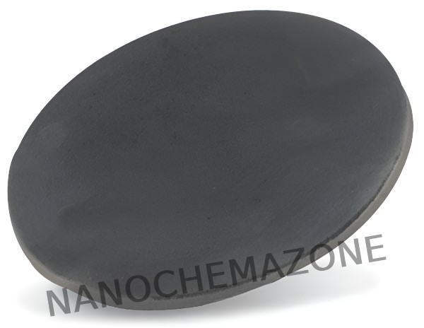
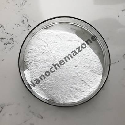
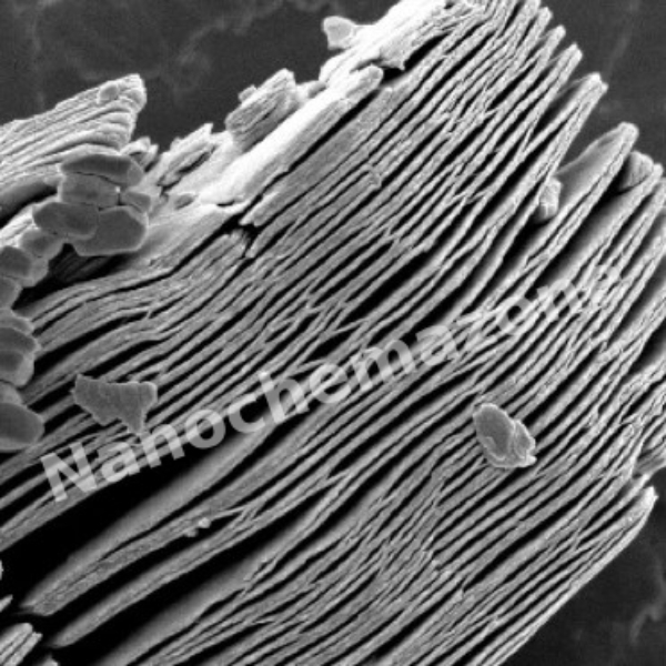
Zirconium Carbide (ZrC) Sputtering Target

Price range: $390.00 through $991.00
Select options This product has multiple variants. The options may be chosen on the product page

Product 

Zirconium Carbide (ZrC) Sputtering Target

CAS No.

 12070-14-3

Appearance

Powder

Purity

≥99%,  ≥99.9%,  ≥95%

(Other purities are also available)

APS

 NA (Size Can be customized), Ask for other available size ranges.

Ingredient

N/A

Molecular Weight

103.23 g/mol

Melting Point

~3,530 °C

Boiling Point

 ~5,100 °C

Density

~6.59 g/cm³

Product Codes

NCZ-1339K

Chitosan(from Mushroom) (236555)

$390.00
Select options This product has multiple variants. The options may be chosen on the product page
Chitosan(from Mushroom) (236555)

ANALYSIS SPECIFICATION
Deacetylation ≥90%
Appearance White or light yellow powder
pH 7-8
Viscosity in 1% Acetic acid ≥15cps
Mesh size 100% pass 80 mesh
Loss on drying ≤8%
Total ash ≤ 2%
Heavy Metals ≤20.0ppm
As ≤ 2.0ppm
Pb ≤ 1.0ppm
Cd ≤ 0.5ppm
Hg ≤ 0.5ppm
Microbiological quality Total Plate Count Yeast & Mold E.Coli. Salmonella . <1000cfu/g <100cfu/g Negative Negative
  Product Codes- NCZ-2661K

beta-Arbutin (439513)

$391.00
Select options This product has multiple variants. The options may be chosen on the product page
beta-Arbutin (439513)
Synonym  Arbutine, arbutin, ursin Chemical name 4-Hydroxyphenyl-beta-D-glucopyranoside CAS# 497-76-7 Physical and chemical properties Appearance: White powder. Infrared signature peak: 1515cm-1 1220cm-1 1050±(5~8)cm-1 Melting point/Melting range:195~199℃. Boiling point/Boiling range: Not available. pH (1% soln/water): 5.0 ~ 7.0 Solubility: Soluble in water, methanol or alcohol. Partially soluble in cold water. Insoluble in aether, chloroform or benzene. Specification Arbutin more than 99.5%. Hydroquinone less than 10 ppm.
Product Codes- NCZ-2707K

Tantalum (Ta) Sputtering Targets, elastomer, Purity: 99.95%, Size: 2”, Thickness: 0.125”

$392.00

Applications of Sputtering Targets;

Film deposition is accomplished using sputtering targets. A technique for sputtering thin films is called "deposition made by sputter targets," which entails eroding material from a "target" source onto a "substrate" like a silicon wafer. Etching of the target is done using semiconductor sputtering targets. When selectivity is not an issue and a high degree of etching anisotropy is required, sputter etching is the method of choice. By removing the target material through etching, sputter targets are also utilized for investigation. In secondary ion spectroscopy (SIMS), one example is when the target material is sputtered at a steady pace. Mass spectrometry is used to quantify the concentration and identity of spewed atoms as the target is sputtered.

The target material's composition may be ascertained and even very low concentrations of contaminants can be found with the aid of the sputtering target.

There is also an application area for sputtering targets in space. One type of space weathering that alters the chemical and physical characteristics of airless worlds like the Moon and asteroids is sputtering.

Titanium Dioxide (TiO2) Sputtering Targets, Purity: 99.9%, Size: 2”, Thickness: 0.250”, Grey to Black

$392.00

Applications of Sputtering Targets;

Film deposition is accomplished using sputtering targets. A technique for sputtering thin films is called "deposition made by sputter targets," which entails eroding material from a "target" source onto a "substrate" like a silicon wafer. Etching of the target is done using semiconductor sputtering targets. When selectivity is not an issue and a high degree of etching anisotropy is required, sputter etching is the method of choice. By removing the target material through etching, sputter targets are also utilized for investigation. In secondary ion spectroscopy (SIMS), one example is when the target material is sputtered at a steady pace. Mass spectrometry is used to quantify the concentration and identity of spewed atoms as the target is sputtered.

The target material's composition may be ascertained and even very low concentrations of contaminants can be found with the aid of the sputtering target.

There is also an application area for sputtering targets in space. One type of space weathering that alters the chemical and physical characteristics of airless worlds like the Moon and asteroids is sputtering.

Tungsten Disulfide (WS2) Sputtering Targets, Purity: 99.9%, Size: 3”, Thickness: 0.125”

$392.00

Applications of Sputtering Targets;

Film deposition is accomplished using sputtering targets. A technique for sputtering thin films is called "deposition made by sputter targets," which entails eroding material from a "target" source onto a "substrate" like a silicon wafer. Etching of the target is done using semiconductor sputtering targets. When selectivity is not an issue and a high degree of etching anisotropy is required, sputter etching is the method of choice. By removing the target material through etching, sputter targets are also utilized for investigation. In secondary ion spectroscopy (SIMS), one example is when the target material is sputtered at a steady pace. Mass spectrometry is used to quantify the concentration and identity of spewed atoms as the target is sputtered.

The target material's composition may be ascertained and even very low concentrations of contaminants can be found with the aid of the sputtering target.

There is also an application area for sputtering targets in space. One type of space weathering that alters the chemical and physical characteristics of airless worlds like the Moon and asteroids is sputtering.

Copper (Cu) Sputtering Targets, Purity: 99.999%, Size: 4”, Thickness: 0.250”

$392.00

Product 

Copper (Cu) Sputtering Targets, Purity: 99.999%, Size: 4'', Thickness: 0.250''

CAS No.

7440-50-8

Appearance

Powder

Purity

≥99%,  ≥99.9%,  ≥95%

(Other purities are also available)

APS

 N/A (Size Can be customized), Ask for other available size ranges.

Ingredient

N/A

Molecular Weight

63.55 g/mol

Melting Point

1,084 °C

Boiling Point

 2,562 °C

Density

8.96 g/cm³

Product Codes

NCZ-2259K

Poly(DL-lactide-co-glycolide)(PLGA50/50) (611989)

$392.00
Poly(DL-lactide-co-glycolide)(PLGA50/50) (611989)
Grade Inherent viscosity (dL/g) Weight average molecular weight (x10000)
PLGA50/50-02 0.1-0.2 0.7-2
PLGA50/50-04 0.2-0.4 2 5
PLGA50/50-06 0.4-0.6
PLGA50/50-08 0.6-0.8 7-10
PLGA50/50-10 0.8-1.0 10-13
Product Codes- NCZ-2635K

Poly(DL-lactide-co-glycolide)(PLGA75/25) (621989)

$392.00
Poly(DL-lactide-co-glycolide)(PLGA75/25) (621989)
Grade Inherent viscosity (d L/g) Weight average molecular weight ("10000)
PLGA75/25-02 0.1-0.2 0.7-2
PLGA75/25-04 0.2-0.4 2-5
PLGA75/25-06 0.4-0.5
PLGA75/25-08 0.6-0.8 7-10
PLGA75/25-10 0.8-1 0 10-13
PLGA75/25-12 1.0 1 2 13 20
PLGA75/25-15 1.2-1.5 20-30
Product Codes- NCZ-2636K

Tantalum Oxide (Ta2O5) Sputtering Targets, Purity: 99.99%, Size: 2”, Thickness: 0.125”

$393.00

Applications of Sputtering Targets;

Film deposition is accomplished using sputtering targets. A technique for sputtering thin films is called "deposition made by sputter targets," which entails eroding material from a "target" source onto a "substrate" like a silicon wafer. Etching of the target is done using semiconductor sputtering targets. When selectivity is not an issue and a high degree of etching anisotropy is required, sputter etching is the method of choice. By removing the target material through etching, sputter targets are also utilized for investigation. In secondary ion spectroscopy (SIMS), one example is when the target material is sputtered at a steady pace. Mass spectrometry is used to quantify the concentration and identity of spewed atoms as the target is sputtered.

The target material's composition may be ascertained and even very low concentrations of contaminants can be found with the aid of the sputtering target.

There is also an application area for sputtering targets in space. One type of space weathering that alters the chemical and physical characteristics of airless worlds like the Moon and asteroids is sputtering.

Tantalum Oxide (Ta2O5) Sputtering Targets, Purity: 99.99%, Size: 2”, Thickness: 0.125”

$393.00

Applications of Sputtering Targets;

Film deposition is accomplished using sputtering targets. A technique for sputtering thin films is called "deposition made by sputter targets," which entails eroding material from a "target" source onto a "substrate" like a silicon wafer. Etching of the target is done using semiconductor sputtering targets. When selectivity is not an issue and a high degree of etching anisotropy is required, sputter etching is the method of choice. By removing the target material through etching, sputter targets are also utilized for investigation. In secondary ion spectroscopy (SIMS), one example is when the target material is sputtered at a steady pace. Mass spectrometry is used to quantify the concentration and identity of spewed atoms as the target is sputtered.

The target material's composition may be ascertained and even very low concentrations of contaminants can be found with the aid of the sputtering target.

There is also an application area for sputtering targets in space. One type of space weathering that alters the chemical and physical characteristics of airless worlds like the Moon and asteroids is sputtering.

Chromium Oxide (Cr2O3) Sputtering Targets, Purity: 99.8%-99.9%, Size: 1”, Thickness: 0.250”

$393.00

Product 

Chromium Oxide (Cr2O3) Sputtering Targets, Purity: 99.8%-99.9%, Size: 1'', Thickness: 0.250''

CAS No.

1308-38-9

Appearance

Powder

Purity

≥99%,  ≥99.9%,  ≥95%

(Other purities are also available)

APS

 N/A (Size Can be customized), Ask for other available size ranges.

Ingredient

N/A

Molecular Weight

 151.99 g/mol

Melting Point

2,435 °C

Boiling Point

 ~3,000 °C (approximate; may decompose before boiling)

Density

5.21 g/cm³

Product Codes

NCZ-2305K

Nickel (Ni) Sputtering Targets, Purity: 99.995%, Size: 8”, Thickness: 0.125”

$394.00

Applications of Sputtering Targets;

Film deposition is accomplished using sputtering targets. A technique for sputtering thin films is called "deposition made by sputter targets," which entails eroding material from a "target" source onto a "substrate" like a silicon wafer. Etching of the target is done using semiconductor sputtering targets. When selectivity is not an issue and a high degree of etching anisotropy is required, sputter etching is the method of choice. By removing the target material through etching, sputter targets are also utilized for investigation. In secondary ion spectroscopy (SIMS), one example is when the target material is sputtered at a steady pace. Mass spectrometry is used to quantify the concentration and identity of spewed atoms as the target is sputtered.

The target material's composition may be ascertained and even very low concentrations of contaminants can be found with the aid of the sputtering target.

There is also an application area for sputtering targets in space. One type of space weathering that alters the chemical and physical characteristics of airless worlds like the Moon and asteroids is sputtering.

Titanium Nitride (TiN) Sputtering Targets, Purity: 99.5%, Size: 1”, Thickness: 0.250”

$394.00

Applications of Sputtering Targets;

Film deposition is accomplished using sputtering targets. A technique for sputtering thin films is called "deposition made by sputter targets," which entails eroding material from a "target" source onto a "substrate" like a silicon wafer. Etching of the target is done using semiconductor sputtering targets. When selectivity is not an issue and a high degree of etching anisotropy is required, sputter etching is the method of choice. By removing the target material through etching, sputter targets are also utilized for investigation. In secondary ion spectroscopy (SIMS), one example is when the target material is sputtered at a steady pace. Mass spectrometry is used to quantify the concentration and identity of spewed atoms as the target is sputtered.

The target material's composition may be ascertained and even very low concentrations of contaminants can be found with the aid of the sputtering target.

There is also an application area for sputtering targets in space. One type of space weathering that alters the chemical and physical characteristics of airless worlds like the Moon and asteroids is sputtering.

Molybdenum Disulfide (MoS2) Sputtering Target

Price range: $394.00 through $989.00
Select options This product has multiple variants. The options may be chosen on the product page

Product 

Molybdenum Disulfide (MoS2) Sputtering Target

CAS No.

1317-33-5

Appearance

Powder

Purity

≥99%,  ≥99.9%,  ≥95%

(Other purities are also available)

APS

 NA (Size Can be customized), Ask for other available size ranges.

Ingredient

N/A

Molecular Weight

160.07 g/mol

Melting Point

~1,185 °C

Boiling Point

Sublimes (>2,000 °C)

Density

 ~5.06 g/cm³

Product Codes

NCZ-1342K

Nickel (Ni) Sputtering Targets, Purity: 99.99%, Size: 6”, Thickness: 0.250”

$394.00

Product 

Nickel (Ni) Sputtering Targets, Purity: 99.99%, Size: 6'', Thickness: 0.250''

CAS No.

7440-02-0

Appearance

Powder

Purity

≥99%,  ≥99.9%,  ≥95%

(Other purities are also available)

APS

 N/A (Size Can be customized), Ask for other available size ranges.

Ingredient

N/A

Molecular Weight

 58.69 g/mol

Melting Point

 1,455 °C

Boiling Point

 2,732 °C

Density

 8.90 g/cm³

Product Codes

NCZ-1869K

Germanium (Ge) Sputtering Targets, Purity: 99.999%, Size: 3”, Thickness: 0.125”

$394.00

Product 

Germanium (Ge) Sputtering Targets, Purity: 99.999%, Size: 3'', Thickness: 0.125''

CAS No.

7440-56-4

Appearance

Powder

Purity

≥99%,  ≥99.9%,  ≥95%

(Other purities are also available)

APS

 N/A (Size Can be customized), Ask for other available size ranges.

Ingredient

N/A

Molecular Weight

 72.63 g/mol

Melting Point

 938.3 °C

Boiling Point

2,833 °C

Density

 5.32 g/cm³

Product Codes

NCZ-2240K

Lead (Pb) Sputtering Targets, Purity: 99.99+%, Size: 4”, Thickness: 0.250”

$395.00

Product 

Lead (Pb) Sputtering Targets, Purity: 99.99+%, Size: 4'', Thickness: 0.250''

CAS No.

7439‑92‑1

Appearance

Powder

Purity

≥99%,  ≥99.9%,  ≥95%

(Other purities are also available)

APS

 N/A (Size Can be customized), Ask for other available size ranges.

Ingredient

N/A

Molecular Weight

 207.2 g/mol

Melting Point

~327.5 °C

Boiling Point

~1,740 °C

Density

 ~11.34 g/cm³

Product Codes

NCZ-2071K

Sodium Hyaluronate(powder, Eyedrop grade, ≥95%) (337644)

$395.00
Select options This product has multiple variants. The options may be chosen on the product page
Sodium Hyaluronate(powder, Eyedrop grade, ≥95%) (337644)
  Specifications
Test Items Standard
Appearance White powder
Hyaluronic acid ≥95%
Molecular weight (0.5-1.0) x 106
Chlorides ≤0.5
pH 5.5-8.0
Iron <80ppm
Loss on drying ≤10%
Protein ≤0.1%
Nitrogen 3.0%-4.0%
Heavy metal ≤10ppm
Bacterial counts ≤100cfu/g
Mold and Yeast ≤10cfu/g
Endotoxin ≤0. 5eu/mg
Nucleic Acids (A260nm) <0.5
Sterile Test Complies
    Product Codes- NCZ-2704K

QUICK VIEW Lanthanum Strontium Manganate (La0.9Sr0.1MnO3) Sputtering Targets, Purity: 99.9%, Size: 1”, Thickness: 0.250”

$396.00

Applications of Sputtering Targets;

  • Sputtering targets is used for film deposition. The deposition made by sputter targets is a method of depositing thin films by sputtering that involves eroding material from a "target" source onto a "substrate" such as  a silicon wafer.
  • Semiconductor sputtering targets is used to etch the target. Sputter etching is chosen in cases where a high degree of etching anisotropy is needed and selectivity is not a concern.
  • Sputter targets is also used for analysis by etching away the target material.
One of the example occurs in secondary ion spectroscopy (SIMS), where the target sample is sputtered at a constant rate. As the target is sputtered, the concentration and identity of sputtered atoms are measured using mass spectrometry. By helping of the sputtering target, the composition of the target material can be determined and even extremely low concentrations of impurities are detected. Sputtering target has also application area in space. Sputtering is one of the forms of space weathering, a process that changes the physical and chemical properties of airless bodies, such as asteroids and the Moon.

Boron Nitride (BN) Sputtering Targets, Purity: 99.5%, Size: 2”, Thickness: 0.125”

$396.00

Applications of Sputtering Targets;

Film deposition is accomplished using sputtering targets. A technique for sputtering thin films is called "deposition made by sputter targets," which entails eroding material from a "target" source onto a "substrate" like a silicon wafer. Etching of the target is done using semiconductor sputtering targets. When selectivity is not an issue and a high degree of etching anisotropy is required, sputter etching is the method of choice. By removing the target material through etching, sputter targets are also utilized for investigation.

In secondary ion spectroscopy (SIMS), one example is when the target material is sputtered at a steady pace. Mass spectrometry is used to quantify the concentration and identity of spewed atoms as the target is sputtered. The target material's composition may be ascertained and even very low concentrations of contaminants can be found with the aid of the sputtering target.

There is also an application area for sputtering targets in space. One type of space weathering that alters the chemical and physical characteristics of airless worlds like the Moon and asteroids is sputtering.

5N (99.999%) Boron (B) 3-8mm Pieces Evaporation Materials

Price range: $396.00 through $975.00
Select options This product has multiple variants. The options may be chosen on the product page
Product 5N (99.999%) Boron (B) 3-8mm Pieces Evaporation Materials
CAS No. 7440-42-8
Appearance Black, Semi-metallic
Purity ≥99%,  ≥99.9%,  ≥95%(Other purities are also available)
APS 3–8mm (Size Can be customized),  Ask for other available size range.
Ingredient B
Molecular Weight 10.81 g/mol
Melting Point 2,079 °C
Boiling Point N/A
Density 2.34 g/cm3
Product Codes NCZ-144E
 

10mL Triangular Gold (Au) Nanoplates Water Dispersion, 140±25nm

$396.00
Product 10mL Triangular Gold (Au) Nanoplates Water Dispersion, 140±25nm
CAS No. 7440-22-4
Appearance Deep red, purple, violet, or blue
Purity ≥99%,  ≥99.9%,  ≥95%(Other purities are also available)
APS 140 ± 25nm (Size Can be customized),  Ask for other available size range.
Ingredient Au
Molecular Weight 196.97 g/mol
Melting Point 1064 °C
Boiling Point 2966 – 3080 °C
Density 19.32 g/cm³
Product Codes NCZ-131I

5N (99.999%) Boron (B) 3-8mm Pieces Evaporation Materials

Price range: $396.00 through $975.00
Select options This product has multiple variants. The options may be chosen on the product page
Product 5N (99.999%) Boron (B) 3-8mm Pieces Evaporation Materials
CAS No. 7440-42-8
Appearance Black, brittle crystalline solid
Purity ≥99%,  ≥99.9%,  ≥95%(Other purities are also available)
APS 3-8mm (Size Can be customized),  Ask for other available size range.
Ingredient B
Molecular Weight 10.81 g/mol
Melting Point 2,076 °C
Boiling Point 3927 °C
Density 2.34 g/cm³
Product Codes NCZ-196I
 

Molybdenum Oxide (MoO3) Sputtering Targets, Purity: 99.9%, Size: 2”, Thickness: 0.125”

$397.00

Applications of Sputtering Targets;

Film deposition is accomplished using sputtering targets. A technique for sputtering thin films is called "deposition made by sputter targets," which entails eroding material from a "target" source onto a "substrate" like a silicon wafer. Etching of the target is done using semiconductor sputtering targets. When selectivity is not an issue and a high degree of etching anisotropy is required, sputter etching is the method of choice. By removing the target material through etching, sputter targets are also utilized for investigation. In secondary ion spectroscopy (SIMS), one example is when the target material is sputtered at a steady pace. Mass spectrometry is used to quantify the concentration and identity of spewed atoms as the target is sputtered.

By helping of the sputtering target, the composition of the target material may be evaluated and even extremely tiny amounts of contaminants are recognized.

There is also an application area for sputtering targets in space. One type of space weathering that alters the chemical and physical characteristics of airless worlds like the Moon and asteroids is sputtering.

Silicon Nitride (Si3N4) Sputtering Targets, Purity: 99.5%, Size: 2”, Thickness: 0.125”, Dark Gray to Black

$397.00

Applications of Sputtering Targets;

Film deposition is accomplished using sputtering targets. A technique for sputtering thin films is called "deposition made by sputter targets," which entails eroding material from a "target" source onto a "substrate" like a silicon wafer. Etching of the target is done using semiconductor sputtering targets. When selectivity is not an issue and a high degree of etching anisotropy is required, sputter etching is the method of choice. By removing the target material through etching, sputter targets are also utilized for investigation. In secondary ion spectroscopy (SIMS), one example is when the target material is sputtered at a steady pace. Mass spectrometry is used to quantify the concentration and identity of spewed atoms as the target is sputtered.

The target material's composition may be ascertained and even very low concentrations of contaminants can be found with the aid of the sputtering target.

There is also an application area for sputtering targets in space. One type of space weathering that alters the chemical and physical characteristics of airless worlds like the Moon and asteroids is sputtering.

Silicon Nitride (Si3N4) Sputtering Targets, Purity: 99.5%, Size: 2”, Thickness: 0.125”, Dark Gray to Black

$397.00

Applications of Sputtering Targets;

Film deposition is accomplished using sputtering targets. A technique for sputtering thin films is called "deposition made by sputter targets," which entails eroding material from a "target" source onto a "substrate" like a silicon wafer. Etching of the target is done using semiconductor sputtering targets. When selectivity is not an issue and a high degree of etching anisotropy is required, sputter etching is the method of choice. By removing the target material through etching, sputter targets are also utilized for investigation. In secondary ion spectroscopy (SIMS), one example is when the target material is sputtered at a steady pace. Mass spectrometry is used to quantify the concentration and identity of spewed atoms as the target is sputtered.

The target material's composition may be ascertained and even very low concentrations of contaminants can be found with the aid of the sputtering target.

There is also an application area for sputtering targets in space. One type of space weathering that alters the chemical and physical characteristics of airless worlds like the Moon and asteroids is sputtering.

Zinc Oxide (ZnO) Sputtering Targets, Purity: 99.9%, Size: 1”, Thickness: 0.250”

$397.00

Applications of Sputtering Targets;

Film deposition is accomplished using sputtering targets. A technique for sputtering thin films is called "deposition made by sputter targets," which entails eroding material from a "target" source onto a "substrate" like a silicon wafer. Etching of the target is done using semiconductor sputtering targets. When selectivity is not an issue and a high degree of etching anisotropy is required, sputter etching is the method of choice. By removing the target material through etching, sputter targets are also utilized for investigation. In secondary ion spectroscopy (SIMS), one example is when the target material is sputtered at a steady pace. Mass spectrometry is used to quantify the concentration and identity of spewed atoms as the target is sputtered.

The target material's composition may be ascertained and even very low concentrations of contaminants can be found with the aid of the sputtering target.

There is also an application area for sputtering targets in space. One type of space weathering that alters the chemical and physical characteristics of airless worlds like the Moon and asteroids is sputtering.

Zinc Oxide (ZnO) with Alumina Sputtering Targets, Purity: 99.99%, Size: 3”, Thickness: 0.125”

$397.00

Applications of Sputtering Targets;

Film deposition is accomplished using sputtering targets. A technique for sputtering thin films is called "deposition made by sputter targets," which entails eroding material from a "target" source onto a "substrate" like a silicon wafer. Etching of the target is done using semiconductor sputtering targets. When selectivity is not an issue and a high degree of etching anisotropy is required, sputter etching is the method of choice. By removing the target material through etching, sputter targets are also utilized for investigation. In secondary ion spectroscopy (SIMS), one example is when the target material is sputtered at a steady pace. Mass spectrometry is used to quantify the concentration and identity of spewed atoms as the target is sputtered.

The target material's composition may be ascertained and even very low concentrations of contaminants can be found with the aid of the sputtering target.

There is also an application area for sputtering targets in space. One type of space weathering that alters the chemical and physical characteristics of airless worlds like the Moon and asteroids is sputtering.

Permalloy (Ni-Fe-Mo) Sputtering Targets, Size: 3”, Thickness: 0.125”

$397.00

Product 

Permalloy (Ni-Fe-Mo) Sputtering Targets, Size: 3'', Thickness: 0.125''

CAS No.

 Nickel: 7440-02-0 Iron: 7439-89-6 Molybdenum: 7439-98-7

Appearance

Powder

Purity

≥99%,  ≥99.9%,  ≥95%

(Other purities are also available)

APS

N/A (Size Can be customized), Ask for other available size ranges.

Ingredient

N/A

Molecular Weight

 Not defined (alloy), but elemental weights: Ni: 58.69 g/mol Fe: 55.85 g/mol Mo: 95.95 g/mol

Melting Point

 ~1450 °C

Boiling Point

 ~2730–3000 °C

Density

~8.7 g/cm³

Product Codes

NCZ-1799K

Tantalum Nanoparticles/ Nanopowder ( Ta, 99.7% 60-80 nm)

Price range: $398.00 through $1,287.00
Select options This product has multiple variants. The options may be chosen on the product page
$398/25g
$1287/100g

Product 

Tantalum Nanoparticles/ Nanopowder ( Ta, 99.7% 60-80 nm)

CAS No.

7440-25-7

Appearance

Powder

Purity

≥99%,  ≥99.9%,  ≥95%

(Other purities are also available)

APS

60-80 nm (Size Can be customized), Ask for other available size ranges.

Ingredient

N/A

Molecular Weight

180.95 g/mol

Melting Point

3,017 °C

Boiling Point

5,458 °C

Density

16.69 g/cm³

Product Codes

NCZ-1076K

Indium Phosphide (InP) Wafers, Size: 2”, Thickness: 350± 25 μm, Orientation: 111, Single Side Polished, EPI-Ready

Price range: $399.00 through $1,820.00
Select options This product has multiple variants. The options may be chosen on the product page
1 piece/360  5 pieces/1640                           Please contact us for quotes on larger quantities !!!

Indium Phosphide (InP) Wafers

Size: 2'', Thickness: 350±25 μm, Orientation: 111

Technical Properties:

Size (inch)  2”
Thickness (μm)  350± 25
Dopant  Sulphur (N type)
Polished  Single Side
Mobility (1.5-3.5)E3
Orientation  111
EPD  ≤5000
Growth method  VGF
OF Length  16±2
IF Length   8±1

Fields of Application for Indium Phosphide (InP)

Indium phosphide (InP) is a binary semiconductor composed of indium and phosphorus. Indium phosphide (InP) has started to be developed at the beginning of 1980s. Indium phosphide (InP) which used in a high power and high frequency electronics, has superior electron velocity. Indium phosphide (InP) has a direct bandgap by contrast with many semiconductors. This makes indium phosphide (InP) useful for optoelectronics and laser diodes. Indium phosphide (InP) is a crucial material for production of laser signals, determination and conversion of those signals back to electronic form. Indium Phopshide (InP) is a binary semiconductor composed of Indium (In) and Phosphorus (P), belonging to a group of materials commonly known as III-V Semiconductors. InP is used in high power and high-frequency electronics and boasts a superior electron velocity in comparison to more common semiconductors such as Silicon and Gallium Arsenide. Indium Phosphide has a face-centred cubic crystal structure almost identical to that of GaAs and most of the lll-V semiconductors. InP wafers must be prepared prior to device fabrication, all III-V wafers must be lapped to remove surface damage that occurs during the slicing process. Wafers are then Chemically Mechanically Polished/Plaranrized (CMP) for the final material removal stage allowing for the attainment of super-flat mirror like surfaces with a remaining roughness on an atomic scale. The wafer is then ready for device fabrication.
  • Indium phosphide (InP) is used in photo-detectors.
  • Indium phosphide (InP) is used in LEDs.
  • Indium phosphide (InP) is used in fiber communications components.
  • Indium phosphide (InP) is used in semiconductor optical amplifiers.

Indium Phosphide (InP) Wafers, Size: 2”, Thickness: 350±25 μm, Orientation: 100, Single Side Polished, EPI-Ready

Price range: $399.00 through $1,820.00
Select options This product has multiple variants. The options may be chosen on the product page
1 piece/360  5 pieces/1640                            Please contact us for quotes on larger quantities !!!

Indium Phosphide (InP) Wafers

Size: 2'', Thickness: 350±25 μm, Orientation: 100

Technical Properties:

Size (inch)  2”
Thickness (μm)  350± 25
Dopant  Sulphur (N type)
Polished  Single Side
Mobility (1.5-3.5)E3
Orientation  100
EPD  ≤5000
Growth method  VGF
OF Length  16±2
IF Length   8±1

Fields of Application for Indium Phosphide (InP)

Indium phosphide (InP) is a binary semiconductor composed of indium and phosphorus. Indium phosphide (InP) has started to be developed at the beginning of 1980s. Indium phosphide (InP) which used in a high power and high frequency electronics, has superior electron velocity. Indium phosphide (InP) has a direct bandgap by contrast with many semiconductors. This makes indium phosphide (InP) useful for optoelectronics and laser diodes. Indium phosphide (InP) is a crucial material for production of laser signals, determination and conversion of those signals back to electronic form. Indium Phopshide (InP) is a binary semiconductor composed of Indium (In) and Phosphorus (P), belonging to a group of materials commonly known as III-V Semiconductors. InP is used in high power and high-frequency electronics and boasts a superior electron velocity in comparison to more common semiconductors such as Silicon and Gallium Arsenide. Indium Phosphide has a face-centred cubic crystal structure almost identical to that of GaAs and most of the lll-V semiconductors. InP wafers must be prepared prior to device fabrication, all III-V wafers must be lapped to remove surface damage that occurs during the slicing process. Wafers are then Chemically Mechanically Polished/Plaranrized (CMP) for the final material removal stage allowing for the attainment of super-flat mirror like surfaces with a remaining roughness on an atomic scale. The wafer is then ready for device fabrication.
  • Indium phosphide (InP) is used in modulators.
  • Indium phosphide (InP) is used in photo-detectors.
  • Indium phosphide (InP) is used in LEDs.
  • Indium phosphide (InP) is used in fiber communications components.
  • Indium phosphide (InP) is used in semiconductor optical amplifiers.

4N (99.99%) Strontium Fluoride (SrF2) Pieces (1-10mm) Evaporation Materials, 100g

$400.00
Select options This product has multiple variants. The options may be chosen on the product page
Product 4N (99.99%) Strontium Fluoride (SrF2) Pieces (1-10mm) Evaporation Materials, 100g
CAS No. 7783-48-4
Appearance Light Yellow Crystal Granule 
Purity ≥99%,  ≥99.9%,  ≥95%(Other purities are also available)
APS 1-10mm (Size Can be customized),  Ask for other available size range.
Ingredient SrF2
Molecular Weight 125.62 g/mol
Melting Point 1,450°C
Boiling Point 2,460°C
Density 4.26 g/cm³
Product Codes NCZ-116E

4N (99.99%) Strontium Fluoride (SrF2) Pieces (1-10mm) Evaporation Materials, 100g

$400.00
Product 4N (99.99%) Strontium Fluoride (SrF2) Pieces (1-10mm) Evaporation Materials, 100g
CAS No. 7783-48-4
Appearance Light Yellow Crystal Granule
Purity ≥99%,  ≥99.9%,  ≥95%(Other purities are also available)
APS 1-10mm (Size Can be customized),  Ask for other available size range.
Ingredient SrF2
Molecular Weight N/A
Melting Point N/A
Boiling Point N/A
Density 4.269 g/cm³
Product Codes NCZ-173I

Niobium Oxide (Nb2O5) Sputtering Targets, Purity: 99.5%, Size: 3”, Thickness: 0.125”

$400.00

Product 

Niobium Oxide (Nb2O5) Sputtering Targets, Purity: 99.5%, Size: 3'', Thickness: 0.125''

CAS No.

1313-96-8

Appearance

Powder

Purity

≥99%,  ≥99.9%,  ≥95%

(Other purities are also available)

APS

N/A (Size Can be customized), Ask for other available size ranges.

Ingredient

N/A

Molecular Weight

 265.81 g/mol

Melting Point

~1512 °C

Boiling Point

N/A

Density

 4.6 – 4.9 g/cm³

Product Codes

NCZ-1808K

Yttrium (Y) Sputtering Targets, Purity: 99.9%, Size: 2”, Thickness: 0.125”

$401.00

Applications of Sputtering Targets;

  • Sputtering targets is used for film deposition. The deposition made by sputter targets is a method of depositing thin films by sputtering that involves eroding material from a "target" source onto a "substrate" such as  a silicon wafer.
  • Semiconductor sputtering targets is used to etch the target. Sputter etching is chosen in cases where a high degree of etching anisotropy is needed and selectivity is not a concern.
  • Sputter targets is also used for analysis by etching away the target material.
One of the example occurs in secondary ion spectroscopy (SIMS), where the target sample is sputtered at a constant rate. As the target is sputtered, the concentration and identity of sputtered atoms are measured using mass spectrometry. By helping of the sputtering target, the composition of the target material can be determined and even extremely low concentrations of impurities are detected. Sputtering target has also application area in space. Sputtering is one of the forms of space weathering, a process that changes the physical and chemical properties of airless bodies, such as asteroids and the Moon.

Zinc (Zn) Sputtering Targets, indium, Purity: 99.99%, Size: 1”, Thickness: 0.125”

$401.00

Product 

Zinc (Zn) Sputtering Targets, indium, Purity: 99.99%, Size: 1'', Thickness: 0.125''

CAS No.

7440‑66‑6

Appearance

Powder

Purity

≥99%,  ≥99.9%,  ≥95%

(Other purities are also available)

APS

Zn (black granules) (Size Can be customized), Ask for other available size ranges.

Ingredient

N/A

Molecular Weight

65.38 g/mol

Melting Point

419.5 °C

Boiling Point

 907 °C

Density

7.14 g/cm³

Product Codes

NCZ-1462K

Silicon (Si) Sputtering Targets, undoped, Purity: 99.999%, Size: 3”, Thickness: 0.125”

$401.00

Product 

Silicon (Si) Sputtering Targets, undoped, Purity: 99.999%, Size: 3'', Thickness: 0.125''

CAS No.

7440-21-3

Appearance

Powder

Purity

≥99%,  ≥99.9%,  ≥95%

(Other purities are also available)

APS

N/A  (Size Can be customized), Ask for other available size ranges.

Ingredient

N/A

Molecular Weight

28.0855 g/mol

Melting Point

1,414 °C

Boiling Point

 3,265 °C

Density

 2.33 g/cm³

Product Codes

NCZ-1733K

Titanium Dioxide (TiO2) Sputtering Targets, Purity: 99.9%, Size: 2”, Thickness: 0.125”, Grey to Black

$402.00

Product 

Titanium Dioxide (TiO2) Sputtering Targets, Purity: 99.9%, Size: 2'', Thickness: 0.125'', Grey to Black

CAS No.

13463‑67‑7

Appearance

Powder

Purity

≥99%,  ≥99.9%,  ≥95%

(Other purities are also available)

APS

TiO₂ (black granules) (Size Can be customized), Ask for other available size ranges.

Ingredient

N/A

Molecular Weight

79.94 g/mol

Melting Point

~1,843 °C

Boiling Point

~2,972 °C

Density

~4.23 g/cm³

Product Codes

NCZ-1441K

Copper (Cu) Sputtering Targets, Purity: 99.99%, Size: 5”, Thickness: 0.250”

$402.00

Product 

Copper (Cu) Sputtering Targets, Purity: 99.99%, Size: 5'', Thickness: 0.250''

CAS No.

7440-50-8

Appearance

Powder

Purity

≥99%,  ≥99.9%,  ≥95%

(Other purities are also available)

APS

 N/A (Size Can be customized), Ask for other available size ranges.

Ingredient

N/A

Molecular Weight

63.55 g/mol

Melting Point

1,084 °C

Boiling Point

 2,562 °C

Density

8.96 g/cm³

Product Codes

NCZ-2258K

Piroctone olamine(octopirox) (677617)

$402.00
Select options This product has multiple variants. The options may be chosen on the product page
Piroctone olamine(octopirox) (677617)

CAS No:68890-66-4

Specifications: Appearance                    White or slightly yellow crystalline powder Odor                                Almost odorless Content                           Not less than 98% Melting point                   130-135℃ Loss on drying                 Not more than 0.3% Ash (SO4)                      Not more than 0.2% pH value (1% aq. solu. 20℃)      8.5-10.0 Heavy metals                   Not more than 20ppm Amino Ethanol                 20.1 to 20.9% dried base
Product Codes- NCZ-2711K

Zinc (Zn) Sputtering Targets, indium, Purity: 99.95%, Size: 2”, Thickness: 0.125”

$403.00

Applications of Sputtering Targets;

Film deposition is accomplished using sputtering targets. A technique for sputtering thin films is called "deposition made by sputter targets," which entails eroding material from a "target" source onto a "substrate" like a silicon wafer. Etching of the target is done using semiconductor sputtering targets. When selectivity is not an issue and a high degree of etching anisotropy is required, sputter etching is the method of choice. By removing the target material through etching, sputter targets are also utilized for investigation. In secondary ion spectroscopy (SIMS), one example is when the target material is sputtered at a steady pace. Mass spectrometry is used to quantify the concentration and identity of spewed atoms as the target is sputtered.

The target material's composition may be ascertained and even very low concentrations of contaminants can be found with the aid of the sputtering target.

There is also an application area for sputtering targets in space. One type of space weathering that alters the chemical and physical characteristics of airless worlds like the Moon and asteroids is sputtering.

Carbon (C) (Pyrolytic Graphite) Sputtering Targets, Purity: 99.999%, Size: 3”, Thickness: 0.125”

$403.00

Product 

Carbon (C) (Pyrolytic Graphite) Sputtering Targets, Purity: 99.999%, Size: 3'', Thickness: 0.125''

CAS No.

 7782-42-5

Appearance

Powder

Purity

≥99%,  ≥99.9%,  ≥95%

(Other purities are also available)

APS

 N/A (Size Can be customized), Ask for other available size ranges.

Ingredient

N/A

Molecular Weight

 12.01 g/mol

Melting Point

Sublimes ~3652 °C (no true melting)

Boiling Point

Sublimes directly ~4,200°C

Density

 ~2.2–2.25 g/cm³

Product Codes

NCZ-2340K

Zinc Oxide (ZnO) Sputtering Targets, Purity: 99.999%, Size: 1”, Thickness: 0.250”

$404.00

Applications of Sputtering Targets;

Film deposition is accomplished using sputtering targets. A technique for sputtering thin films is called "deposition made by sputter targets," which entails eroding material from a "target" source onto a "substrate" like a silicon wafer. Etching of the target is done using semiconductor sputtering targets. When selectivity is not an issue and a high degree of etching anisotropy is required, sputter etching is the method of choice. By removing the target material through etching, sputter targets are also utilized for investigation. In secondary ion spectroscopy (SIMS), one example is when the target material is sputtered at a steady pace. Mass spectrometry is used to quantify the concentration and identity of spewed atoms as the target is sputtered.

The target material's composition may be ascertained and even very low concentrations of contaminants can be found with the aid of the sputtering target.

There is also an application area for sputtering targets in space. One type of space weathering that alters the chemical and physical characteristics of airless worlds like the Moon and asteroids is sputtering.

Iron Oxide (Fe3O4) Sputtering Targets, Purity: 99.9%, Size: 2”, Thickness: 0.125”

$404.00

Product 

Iron Oxide (Fe3O4) Sputtering Targets, Purity: 99.9%, Size: 2'', Thickness: 0.125''

CAS No.

1317‑61‑9

Appearance

Powder

Purity

≥99%,  ≥99.9%,  ≥95%

(Other purities are also available)

APS

 N/A (Size Can be customized), Ask for other available size ranges.

Ingredient

N/A

Molecular Weight

 231.6 g/mol

Melting Point

~1,597 °C

Boiling Point

 ~2,623 °C (material may decompose before boiling)

Density

 ~5.17 g/cm³ (sintered target)

Product Codes

NCZ-2175K

Bismuth (Bi) Sputtering Targets, Purity: 99.999%, Size: 4”, Thickness: 0.250”

$404.00

Product 

Bismuth (Bi) Sputtering Targets, Purity: 99.999%, Size: 4'', Thickness: 0.250''

CAS No.

7440‑69‑9

Appearance

Powder

Purity

≥99%,  ≥99.9%,  ≥95%

(Other purities are also available)

APS

1 – 5 µm (Size Can be customized), Ask for other available size ranges.

Ingredient

N/A

Molecular Weight

~208.98 g/mol

Melting Point

 271.4 °C

Boiling Point

~1560 °C

Density

 ~9.78–9.80 g/cm³

Product Codes

NCZ-2433K

Potassium titanate whisker(K2Ti6O13, D=0.2~1.5µm, L=10~100µm) (222811)

$404.00
Select options This product has multiple variants. The options may be chosen on the product page
Potassium titanate whisker(K2Ti6O13, D=0.2~1.5µm, L=10~100µm) (222811)

Chemical formula: K2Ti6O13 Appearance: white powder Particle shape:  needle crystal Whisker diameter: 0.2-1.5µm Whisker length: 10-100µm Mohs hardness: 4 Bulk density: about 0.3g/cm3 Moisture content: <0.5% pH: 7-9 Heat-resistance: 1200°C(in air) Tensile strength: 7000MPa Elastic modulus: 280GPa

Excellent reflection capacity in infrared region Excellent friction properties: 1. Stable Friction coefficient from room to high temperatures to assure smooth braking. 2. Low Wear at high temperatures, no damage to brake disk 3. Almost no friction noise during braking Applications Reinforcing agent for plastic composites Friction control agent As heat-resistant and insulation paint when mixed with silicon resin
Product Codes- NCZ-2749K

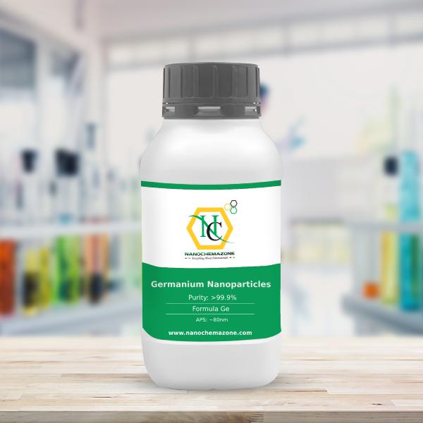
Germanium Nanoparticles/Nanopowder ( Ge, 50~80nm)

Price range: $405.00 through $1,130.00
Select options This product has multiple variants. The options may be chosen on the product page
$450/5g $1130/25g

Product 

Germanium Nanoparticles/Nanopowder ( Ge, 50~80nm)

CAS No.

7440-56-4

Appearance

Powder

Purity

≥99%,  ≥99.9%,  ≥95%

(Other purities are also available)

APS

~80nm (microns) (Size Can be customized), Ask for other available size ranges.

Ingredient

N/A

Molecular Weight

72.63 g/mol

Melting Point

937.4 °C

Boiling Point

2833 °C

Density

~5.32 g/cm³

Product Codes

NCZ-1047K

Indium Bonding on Cu Backing Plate for Sputtering Targets

Price range: $405.00 through $715.00
Select options This product has multiple variants. The options may be chosen on the product page
Product Indium Bonding on Cu Backing Plate for Sputtering Targets
CAS No. 7440-74-6
Appearance Soft, silvery-white metal
Purity ≥99%,  ≥99.9%,  ≥95%(Other purities are also available)
APS N/A
Ingredient In
Molecular Weight N/A
Melting Point 114.82 g/mol
Boiling Point N/A
Density 7.31 g/cm³
Product Codes NCZ-120H

Silicon Carbide (SiC) Sputtering Targets, Purity: 99.5%, Size: 1”, Thickness: 0.125”

$406.00

Applications of Sputtering Targets;

Film deposition is accomplished using sputtering targets. A technique for sputtering thin films is called "deposition made by sputter targets," which entails eroding material from a "target" source onto a "substrate" like a silicon wafer. Etching of the target is done using semiconductor sputtering targets. When selectivity is not an issue and a high degree of etching anisotropy is required, sputter etching is the method of choice. By removing the target material through etching, sputter targets are also utilized for investigation. In secondary ion spectroscopy (SIMS), one example is when the target material is sputtered at a steady pace. Mass spectrometry is used to quantify the concentration and identity of spewed atoms as the target is sputtered.

The target material's composition may be ascertained and even very low concentrations of contaminants can be found with the aid of the sputtering target.

There is also an application area for sputtering targets in space. One type of space weathering that alters the chemical and physical characteristics of airless worlds like the Moon and asteroids is sputtering.

High Purity 99.9wt% Hollow Mesoporous Silica Solution (Spherical)

Price range: $406.00 through $726.00
Select options This product has multiple variants. The options may be chosen on the product page
Product High Purity 99.9wt% Hollow Mesoporous Silica Solution (Spherical)
CAS No. 7631-86-9
Appearance White, opaque solution
Purity ≥99%,  ≥99.9%,  ≥95%(Other purities are also available)
APS 2-50nm (Size Can be customized),  Ask for other available size range.
Ingredient SiO₂
Molecular Weight N/A
Melting Point N/A
Boiling Point N/A
Density N/A
Product Codes NCZ-403I

Polyhydroxylated Fullerene (Fullerenols)/ C60, (-OH) Functionalized, Dispersed in Water, 2000 ppm Dry powder

Price range: $407.00 through $4,938.00
Select options This product has multiple variants. The options may be chosen on the product page

Applications:

1. Pharmaceutical: Diagnostic reagents, super drugs,   cosmetics, nuclear magnetic resonance (NMR) with the developer. DNA affinity, anti-HIV drugs, anti-cancer drugs, chemotherapy drugs, cosmetics additives and scientific research. 2. Energy: Solar battery, fuel cell, secondary battery. 3. Industry: Wear resistant material, flame retardant materials, lubricants, polymer additives, high-performance membrane, catalyst, artificial diamond, hard alloy, electric viscous fluid, ink filters, high-performance coatings, fire retardant coatings, manufacturing bioactive materials , memory materials, embedded molecular and other characteristics, composite materials etc. 4. Information industry: Semiconductor record medium, magnetic materials, printing ink, toner, ink, paper special purposes. 5. Electronic parts: Superconducting semiconductor, diodes, transistors, inductor.  , 6. Optical materials, electronic camera, fluorescence display tube, nonlinear optical materials. 7. Environment: Gas adsorption, gas storage.

Surface Modified Vanadium Carbide (V4C3Tx) MXene Multilayer Nanosheet

Price range: $407.00 through $1,089.00
Select options This product has multiple variants. The options may be chosen on the product page
Product Surface Modified Vanadium Carbide (V4C3Tx) MXene Multilayer Nanosheet
CAS No. 1317-61-9
Appearance Dark gray to black
Purity ≥99%,  ≥99.9%,  ≥95%(Other purities are also available)
APS 10–10nm (Size Can be customized),  Ask for other available size range.
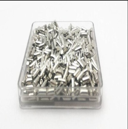
Ingredient V₄C₃Tₓ
Molecular Weight N/A
Melting Point N/A
Boiling Point N/A
Density 2.0–3.5 g/cm³
Product Codes NCZ-547I
 

Ti3C2Tx MXene Multilayer Nanoflakes

Price range: $407.00 through $1,825.00
Select options This product has multiple variants. The options may be chosen on the product page
Product Ti3C2Tx MXene Multilayer Nanoflakes
CAS No. N/A
Appearance Black or dark gray
Purity ≥99%,  ≥99.9%,  ≥95%(Other purities are also available)
APS 0.5–10µm (Size Can be customized),  Ask for other available size range.
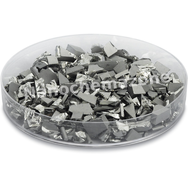
Ingredient Ti₃C₂Tₓ,
Molecular Weight 195.88 g/mol
Melting Point N/A
Boiling Point N/A
Density 3.0–3.5 g/cm³
Product Codes NCZ-561I

Titanate Molecular Sieve (TS-1) Powder, 100-300 nm

Price range: $407.00 through $1,089.00
Select options This product has multiple variants. The options may be chosen on the product page
Product Titanate Molecular Sieve (TS-1) Powder, 100-300 nm
CAS No. 1318-02-1
Appearance Dry, white
Purity ≥99%,  ≥99.9%,  ≥95%(Other purities are also available)
APS 100-300nm (Size Can be customized),  Ask for other available size range.
Ingredient Ti–SiO₂
Molecular Weight 60.08 g/mol
Melting Point N/A
Boiling Point N/A
Density 1.9–2.3 g/cm³
Product Codes NCZ-566I
 

Carbon (C) Sputtering Targets, indium, Purity: 99.999%, Size: 2”, Thickness: 0.125”

$407.00

Product 

Carbon (C) Sputtering Targets, indium, Purity: 99.999%, Size: 2'', Thickness: 0.125''

CAS No.

 7782‑42‑5

Appearance

Powder

Purity

≥99%,  ≥99.9%,  ≥95%

(Other purities are also available)

APS

 N/A (Size Can be customized), Ask for other available size ranges.

Ingredient

N/A

Molecular Weight

12.01 g/mol

Melting Point

Sublimates at ~3,652 °C

Boiling Point

Sublimates at ~4,200 °C

Density

 ~2.25 g/cm³

Product Codes

NCZ-2347K

H-MCM-22(SiO2/Al2O3=26-34) (875940)

$407.00
Select options This product has multiple variants. The options may be chosen on the product page
H-MCM-22(SiO2/Al2O3=26-34) (875940)

SiO2/Al2O3 26-34 Surface area(m2/g) 440 Relative Crystallinity(%) 98 Pore volume(cm3/g) 0.5

Product Codes- NCZ-2719K

Silicon Carbide Wafer (SiC-4H) – 4H, Size: 3”, Thickness: 350 μm, Production Grade, 4H Area: 100%

Price range: $408.00 through $1,863.00
Select options This product has multiple variants. The options may be chosen on the product page
1 piece/370 € 5 pieces/1690 €                 Please contact us for quotes on larger quantities !!!

Silicon Carbide Wafer (SiC-4H)-4H

Size: 3'', Thickness: 350 μm, 4H Area: 100%

Technical Properties:

Quality  Production Grade
Size (inch)  3”
Thickness (μm)  350
Ra  ≤0.3
4H area  100%
Orientation  4°±0.5°
Resistivity   0.015-0.03
TTV  ≤15
Bow  ≤10
Warp  ≤25
OF Length  22.0±2.0
IF Length  11.0±1.5

Fields of Application for Silicon Carbide (SiC-4H)- 4H Wafer

Silicon carbide (SiC) is a rare compound of silicon and carbon which is synthetically produced. Silicon carbide (SiC) crystals have unique physical and electronic properties. Silicon Carbide based devices have been used for short wavelength opto-electronic, high temperature, radiation resistant applications.  The high-power and high-frequency electronic devices made with SiC are superior to Si and GaAs based devices.  Below are some popular applications of SiC substrates. SiC based devices have low lattice mismatch with III-nitride epitaxial layers.  They have high thermal conductivity and can be used for the monitoring of combustion processes and for all sorts of UV-detection.  SiC-based semiconductor devices can work under very hostile environments, such as high temperature, high power, and high radiation conditions. SiC is used for the fabrication of very high-voltage and high-power devices such as diodes, power transistors, and high power microwave devices. Compared to conventional Si-devices, SiC-based power devices have faster switching speed higher voltages, lower parasitic resistances, smaller size, less cooling required due to high-temperature capability. Silicon carbide (SiC) wafer has great electrical properties and excellent thermal properties. Silicon carbide (SiC) wafer has low thermal expansion. Silicon carbide (SiC) wafer has superior hardness properties. Silicon carbide (SiC) wafer performs well at high temperatures. Also, silicon carbide (SiC) wafer has high resistance to corrosion, erosion and oxidation. In addition to, silicon carbide (SiC) wafer is also more shiny than either diamonds or cubic zirconia. While Silicon carbide (SiC-4H) - 4H wafer has superior electronic properties, silicon carbide (SiC-6H) – 6H wafer is most easily prepared and best studied.
  • Silicon carbide (SiC) wafer is used for hybrid and electric vehicles.
  • Silicon carbide (SiC) wafer is used for green energy generation.
  • Silicon carbide (SiC) wafer is used for LEDs.
  • Silicon carbide (SiC) wafer is used for many other emerging markets.
 

Indium Zinc Oxide/IZO (InZnO) Sputtering Targets, Purity: 99.99%, Size: 2”, Thickness: 0.250”

$408.00

Applications of Sputtering Targets;

Film deposition is accomplished using sputtering targets. A technique for sputtering thin films is called "deposition made by sputter targets," which entails eroding material from a "target" source onto a "substrate" like a silicon wafer. Etching of the target is done using semiconductor sputtering targets. When selectivity is not an issue and a high degree of etching anisotropy is required, sputter etching is the method of choice. By removing the target material through etching, sputter targets are also utilized for investigation. In secondary ion spectroscopy (SIMS), one example is when the target material is sputtered at a steady pace. Mass spectrometry is used to quantify the concentration and identity of spewed atoms as the target is sputtered.

The target material's composition may be ascertained and even very low concentrations of contaminants can be found with the aid of the sputtering target.

There is also an application area for sputtering targets in space. One type of space weathering that alters the chemical and physical characteristics of airless worlds like the Moon and asteroids is sputtering.